

Page 1

Ordering number: EN 2148C
°
θ
°
–
°
−
°
2
Thick Film Hybrid IC
STK4065
Car Stereo Use Power Amplifier
(25W min, THD = 10%)
Applications
• Power amplifier for car stereos
• Home karaoke systems
Features
• High output power Maximum output power 40W or
greater (R
35W typ. (R
23W typ. (R
= 2 Ω )
L
= 2 Ω , THD = 10%)
L
= 4 Ω , THD = 10%)
L
• Low distortion
• Built-in protectors
• DC short protector
• Thermal shutdown protector (Thermal protector)
• Overvoltage protector (Overvoltage / power supply
surge protector)
• Audio muting circuit (Fast attack time)
• Free from failure caused by load short
• Wide operating supply voltage range
Specifications
Maximum Ratings
at Ta = 25 ° C
Package Dimensions
unit: mm
4081
[STK4065]
Parameter Symbol Conditions Ratings Unit
V
max(1) Quiescent (circuit cutoff mode) 30s 30 V
CC
Supply voltage
Allowable power dissipation Pd max Infinite heat sink 100 W
Peak output power Po max V
Output current I
Junction temperature Tj 150
Thermal resistance
Operating temperature Topr
Storage temperature Tstg
Available time for load shorted t
V
max(2)
CC
O
j-c 1.25
s
Recommended Operating Conditions
Parameter Symbol Conditions Ratings Unit
Recommended supply voltage V
Load resistance R
CC
L
Operating (f = 100Hz, V
t = 100ms)
= 16V, RL = 2 Ω , f = 1kHz 65 W
CC
V
= ± 13.2V, R
CC
at Ta = 25 ° C
= 1Vrms,
IN
= 2 Ω , f = 50Hz, P
L
18 V
12 A
30 to +85
40 to +125
= 25W 2* s
O
13.2 V
SANYO Electric Co., Ltd. Semiconductor Business Headquarters
TOKYO OFFICE Tokyo Bldg., 1-10, 1 Chome, Ueno, Taito-ku, TOKYO, 110 JAPAN
61197HA (ID) / 80394TH (KOTO) / 1287KI / 4155KI, TS 5-2124 No. 2148—1/9
C
C/W
C
C
Ω
Page 2

∆
−
– ∞ –
–
STK4065
Operating Characteristics
at Ta = 25 ° C, R
= 2 Ω , Rg = 600 Ω , VG = 46dB, V
L
= 13.2V
CC
Parameter Symbol Conditions min typ max Unit
Quiescent current I
Output power
Total harmonic distortion
CCO
P
(1) THD = 10%, f = 1kHz 25 35 – W
O
P
(2) THD = 1%, f = 1kHz – 25 – W
O
P
(3)
O
THD(1) P
THD(2) P
Voltage gain VG P
Frequency response f
Input impedance r
Output noise voltage V
Output offset voltage
, f
L
H
i
NO
V
N
Muting suppression level ATT V
Ripple rejection SVRR
Rg = 10k Ω
THD = 10%, R
f = 1kHz
= 10W, f = 1kHz – 0.06 0.1 %
O
= 1W, f = 20Hz to 20kHz – – 0.3 %
O
= 1W, f = 1kHz 43.8 46.0 48.2 dB
O
P
= 1W, – 10 to 30k – Hz
O
P
= 1W, f = 1kHz 20 30 – k Ω
O
= 4 Ω ,
L
+0
dB
−
3
– 70 140 mA
20 23 – W
Rg = 10k Ω , without BPF – 0.6 1.2 mVrms
Rg = 10k Ω
= +5V
M
f
= 100Hz, Rg = 0 Ω ,
R
V
= 0dBm
R
200 0 +200 mV
dB
–47 – dB
* It is guaranteed that load short causes no damage for 2 seconds. In actual applications, the thermal shutdown protector provides sufficient guarantee against load
short. However, refer to “Notes for Applying the STK4065”, because the saturation current varies with the thermal resistance of the heat sink.
Equivalent Circuit Block Diagram
No. 2148—2/9
Page 3

Test Circuit
STK4065
Notes for Applying the STK4065
(1) V
(2) Protectors
a) Output pin-to-V
The STK4065 contains protectors against output pin-
The output pin-to-V
max
CC
The STK4065 is designed as an amplifier for car use
and its V
max at the operating mode is set to 18V.
CC
When this voltage is exceeded, the overvoltage protector will work to bring the circuit to OFF-state, delivering no output. The overvoltage protector is so designed
as to work at a voltage of 18V to 28V. The protector
works 100% at 28V. When designing an audio set, such
as home stereo, using a transformer power supply, consider AC line regulation and be careful that 18V must
not be exceeded at the quiescent mode. If 18V is
exceeded, the overvoltage protector will w ork, generating an abnormal sound.
short, output pin-to-GND short pro-
CC
tectors
to-V
short and output pin-to-GND short.
CC
short protector works effec-
CC
tively to protect the IC when the power switch is turned
ON at the output pin-to-V
work to protect the IC when output pin-to-V
short state, but does not
CC
short is
CC
forced to be provided at the normal operation mode
after the power switch is turned ON.
The output pin-to-V
short protector is intended to
CC
protect the IC against damage when pin-to-pin short
occurs in the assembly process.
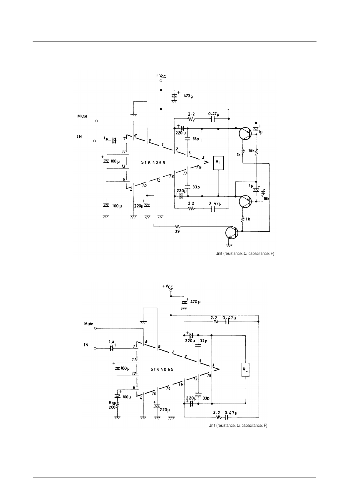
If there is possibility that output pin-to-V
caused by the user, the auxiliary output pin-to-V
short is
CC
CC
short protector shown on page 5 must be connected
externally. The output pin-to-GND short protector
works effectively to protect the IC against damage
when the power switch is turned ON at the output Pinto-GND short state and also when output pin-to-GND
short is forced to be provided at the normal operation
mode after the power switch in turned ON.
b) Thermal shutdown
The STK4065 contains thermal protectors.
The thermal protector detects abnormal temperature
rise caused when the IC operates abnormally (load
short, etc.), limits the input signal, and prevents tem-
perature from rising, preventing the IC from breaking
down in a short time. The thermal protector starts
working at approximately 135 ° C of substrate tempera-
ture Tc and turns OFF the input signal at approxi-
mately 175 ° C.
No. 2148—3/9
Page 4

STK4065
In normal applications, since a heat sink is mounted on
the IC, the substrate temperature does not rise up to a
temperature at which the input signal is turned OFF
completely, but is saturated at a certain temperature.
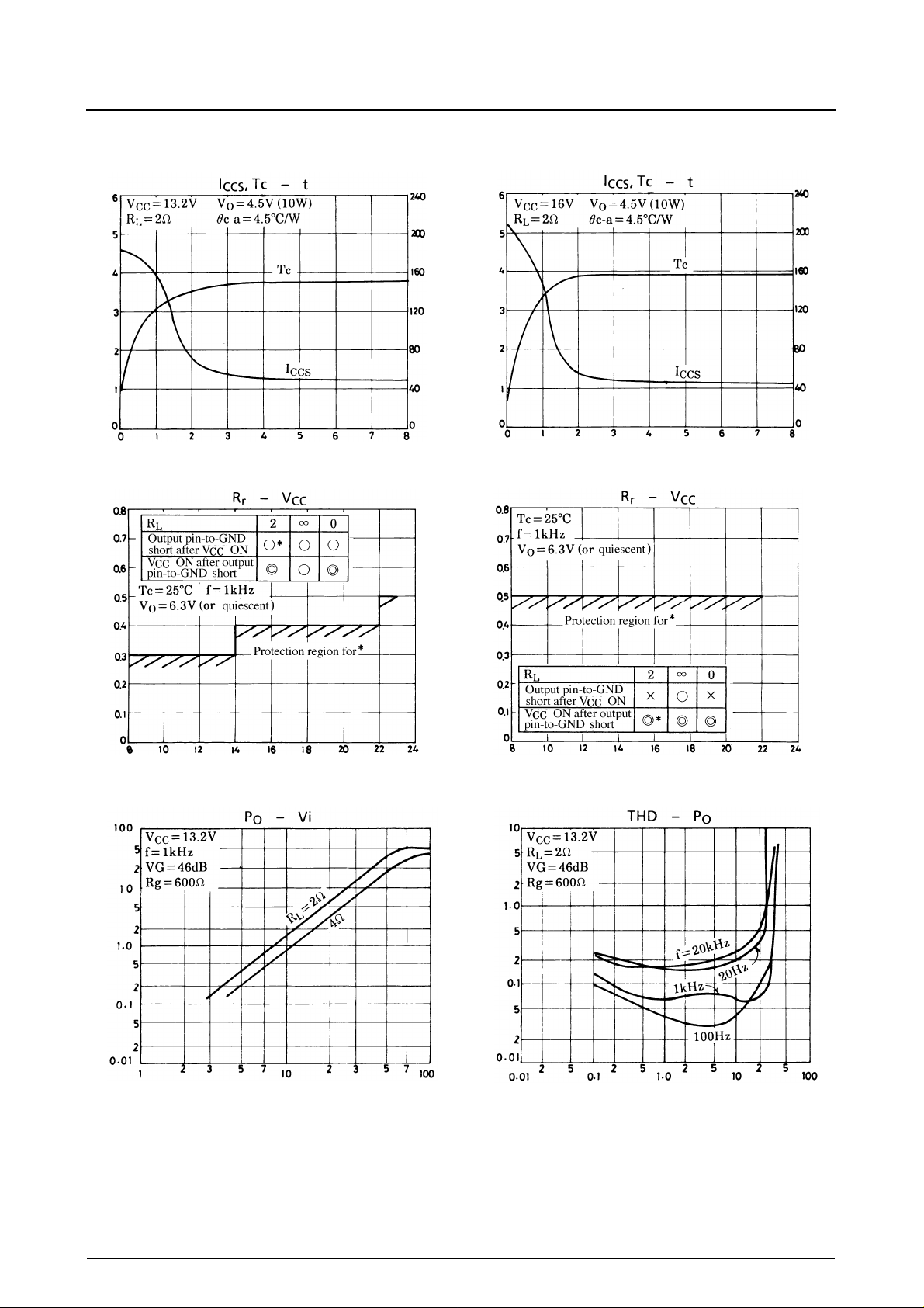
When load short occurs with a heat sink of 4.5 ° C/W
mounted, the substrate temperature is saturated at
approximately 160 ° C.
Tj in this state is as high as 170 ° C, which obviously
exceeds the maximum rating.
As mentioned above, the thermal protector is designed
to prevent the IC from breaking down in a short time
when abnormal temperature rise occurs, but is not
intended to protect the IC from damage for a long time
when abnormal temperature rise occurs.
(3) Others
a) Excessive input
When an excessive input of 1.5 Vrms (f = 1kHz) or
greater is applied to the input pin, the input channel DC
balance of the input monolithic amplifier is disturbed,
the output is cut off, and DC voltage is developed on
the output pins, damaging the speaker. Be careful not
to permit an input of 1.5Vrms (f = 1kHz) or greater to
be applied.
b) Parasitic oscillation
The STK4065 has 2.2 Ω , 0.47 µ F across the V
CC
line
and the bootstrap pins for phase compensation. This
makes it necessary for the power line to be extended
close to the bootstrap pins for both the inverting amplifier and the non-inverting amplifier. Too long a power
line may cause parasitic oscillation to occur at low
temperatures. If so, connect a capacitor of approximately 0.1 µ F across the tip of the power line and GND
to decrease AC impedance of the power line.
c) Inverse application of supply voltage
The STK4065 contains no protector against inverse
application of supply voltage. If there is a possibility
that inverse application of supply voltage may occur,
connect the protector externally.
d) Power switch-OFF mode
Do not connect pin 1 direct to GND, otherwise the IC
may be broken down.
When connecting pin 1 to GND, connect a resistor of
100 Ω or greater in series with pin 1 or connect a diode
across pin 10 and pin 1.
No. 2148—4/9
Page 5
STK4065
Sample Application Circuit of STK4065 Output Pin-to-V
Short Protector
CC
Sample Application of STK4065 VG = 40dB
No. 2148—5/9
Page 6
STK4065
- A
CCS
Load short current, I
Residual resistance, Rr - ΩOutput power, Po - W
Time, t - min
- A
Load short current, I
Substrate temperature, Tc - °C
Residual resistance, Rr - ΩTotal harmonic distortion, THD - %
CCS
Substrate temperature, Tc - °C
Time, t - min
Supply voltage, V
CC
Input voltage, Vi - mV
- V
Supply voltage, V
Output power, Po - W
CC
- V
No. 2148—6/9
Page 7
STK4065
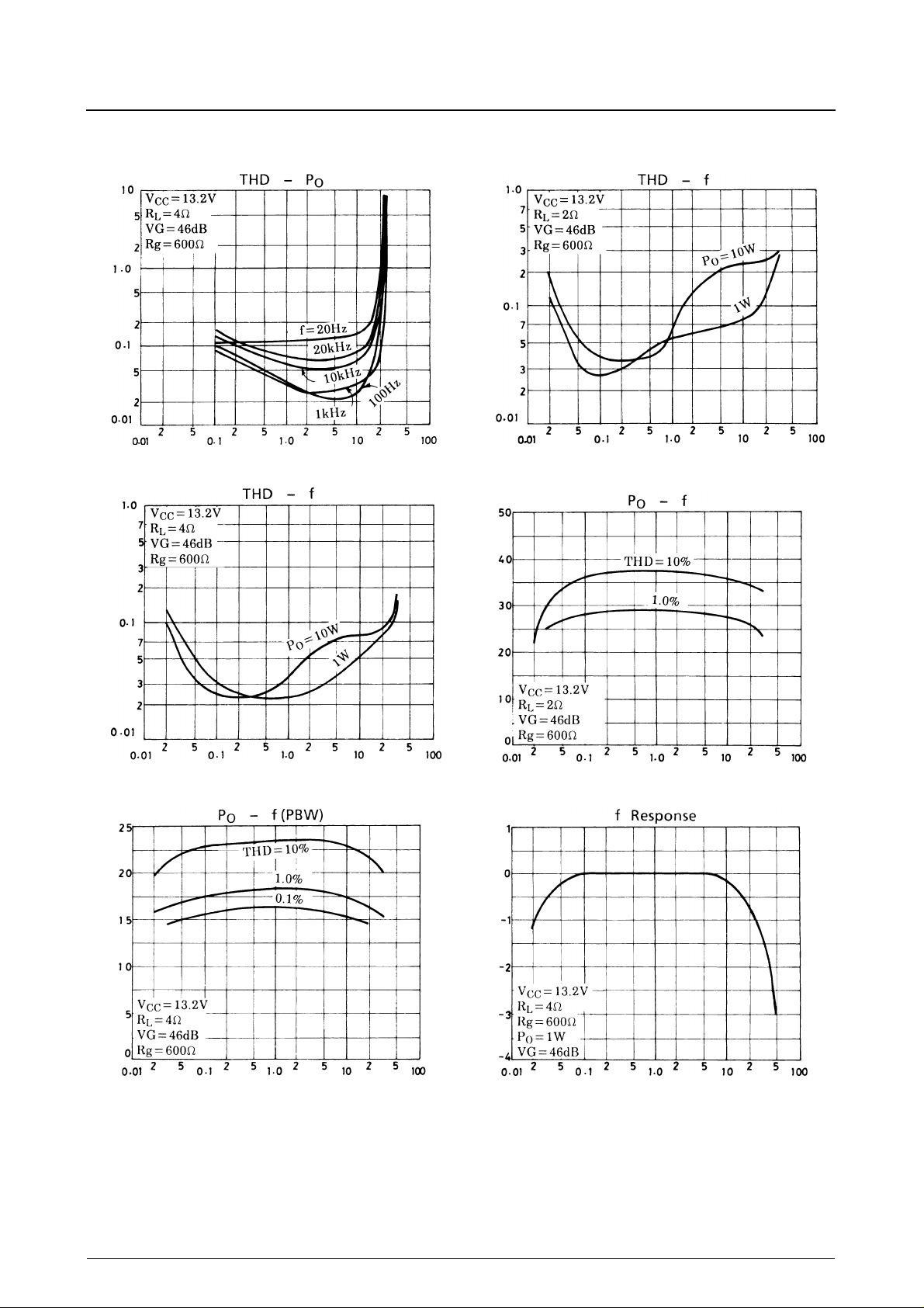
Total harmonic distortion, THD - %Total harmonic distortion, THD - %Output power, Po - W
Output power, Po - W
Frequency, f - Hz
Total harmonic distortion, THD - %Output power, Po - WResponse - dB
Frequency, f - Hz
Frequency, f - Hz
Frequency, f - Hz
Frequency, f - Hz
No. 2148—7/9
Page 8
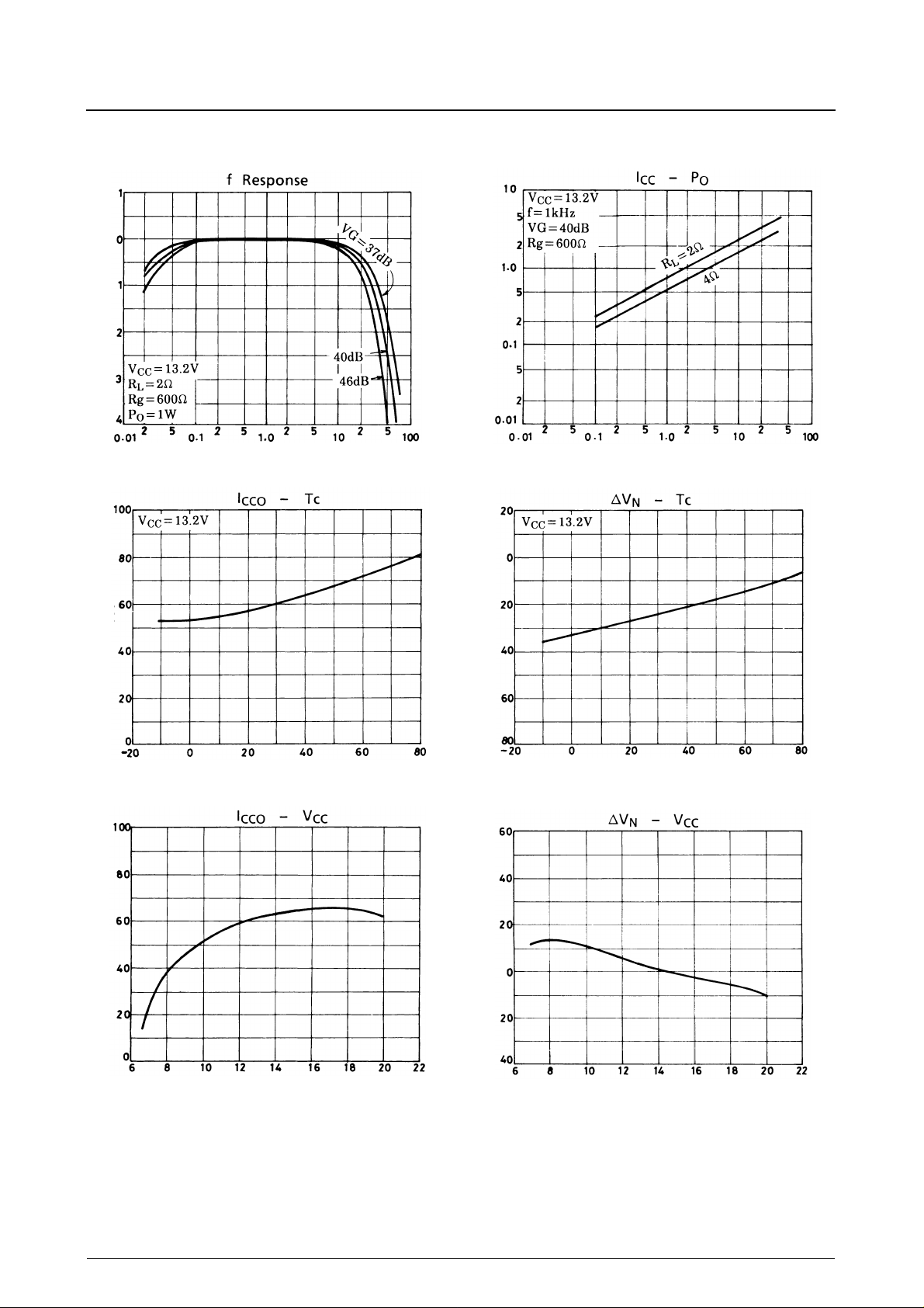
Response - dBQuiescent current, I
STK4065
- mAOutput offset voltage, ∆V
Current drain, I
CC
- mAQuiescent current, I
CCO
- mA
CCO
Frequency, f - Hz
Substrate temperature, Tc - ° C
- mVOutput offset voltage, ∆V
N
- mV
N
Output power, Po - W
Substrate temperature, Tc - ° C
Supply voltage, V
CC
- V
Supply voltage, V
CC
- V
No. 2148—8/9
Page 9
STK4065
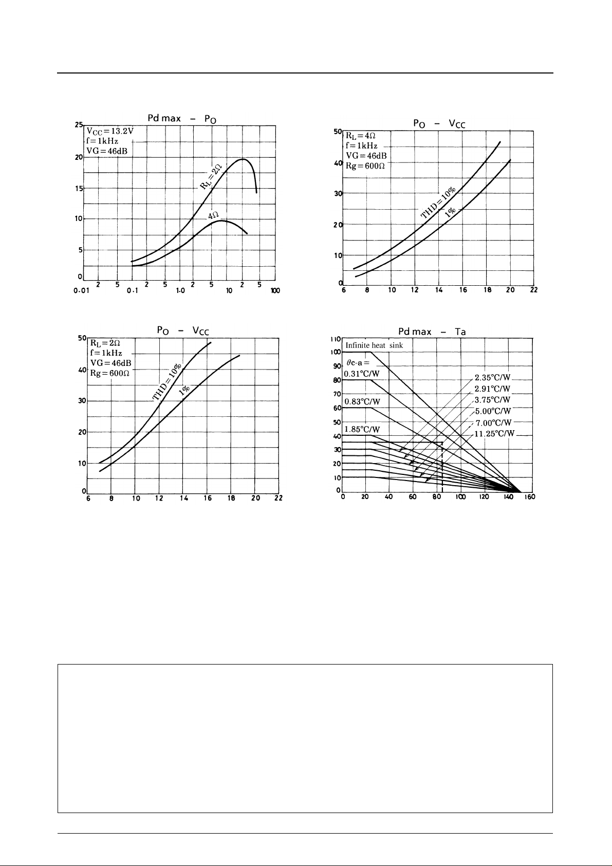
Output power, Po - WIC power dissipation, Pdmax - W
Allowable power dissipation, Pd max - WOutput power, Po - W
Output power, Po - W
Supply voltage, V
CC
- V
Supply voltage, VCC - V
Ambient temperature, Ta - °C
■
No products described or contained herein are intended for use in surgical implants, life-support systems, aerospace equipment, nuclear
power control systems, vehicles, disaster/crime-pre v ention equipment and the lik e, the failure of which may directly or indirectly cause injury,
death or property loss.
■
Anyone purchasing any products described or contained herein for an above-mentioned use shall:
➀
Accept full responsibility and indemnify and defend SANYO ELECTRIC CO., LTD., its affiliates, subsidiaries and distributors and all their
officers and employees, jointly and severally, against any and all claims and litigation and all damages, cost and expenses associated
with such use:
➁
Not impose any responsibility for any fault or negligence which may be cited in any such claim or litigation on SANYO ELECTRIC CO.,
LTD., its affiliates, subsidiaries and distributors or any of their officers and employees, jointly or severally.
■
Information (including circuit diagrams and circuit parameters) herein is for e xample only; it is not guaranteed for volume production. SANYO
believes information herein is accurate and reliable, but no guarantees are made or implied regarding its use or any infringements of
intellectual property rights or other rights of third parties.
This catalog provides information as of June, 1997. Specifications and information herein are subject to change without notice.
No. 2148—9/9
 Loading...