

Page 1

Features
■ Converts low-swing alternating current (AC)
coupled differential input to high-definition
multimedia interface (HDMI) rev 1.3 compliant
■ HDMI level shifting operation up to 2.7 Gbps
per lane
■ Integrated 50 Ω termination resistors for AC-
coupled differential inputs
■ Input/output transition minimized differential
signaling (TMDS) enable/disable
■ Output slew rate control on TMDS outputs to
minimize electromagnetic interference (EMI)
and eliminate external components such as RC
and choke
■ Fail safe outputs for backdrive protection
■ No re-timing or configuration required
■ Inter-pair output skew < 250 ps, intra-pair
output skew < 10 ps
■ Single power supply of 3.3 V
■ ESD protection: ±6 KV HBM on all I/O pins
■ Integrated display data channel (DDC) level
shifters. Pass-gate voltage limiters allow 3.3 V
termination on graphics and memory controller
hub (GMCH) pins and 5 V DDC termination on
HDMI connector pins
■ Level shifter and configurable output for HPD
signal from HDMI/DVI connector
■ Integrated pull-down resistor on HPD_SINK
and OE_N inputs
Applications
■ Notebooks, PC motherboards and graphic
cards
Table 1. Device summary
Order code Package Packing
STHDLS101A
Enhanced AC coupled HDMI level shifter
with configurable HPD output
QFN48
(7x7mm)
Description
The STHDLS101A is a high-speed high-definition
multimedia interface (HDMI) level shifter that
converts low-swing AC coupled differential input
to HDMI 1.3 compliant open-drain current
steering RX-terminated differential output.
Through the existing PCI-E pins in the graphics
and memory controller hub (GMCH) of PCs or
notebook motherboards, the pixel clock provides
the required bandwidth (1.65 Gbps, 2.25 Gbps)
for the video supporting 720p, 1080i, 1080p with a
total of 36-bit resolution. The HDMI is multiplexed
onto the PCIe pins in the motherboard where the
AC coupled HDMI at 1.2 V is output by GMCH.
The AC coupled HDMI is then level shifter by this
device to 3.3 V DC coupled HDMI output.
The STHDLS101A supports up to 2.7 Gbps,
which is enough for 12-bits of color depth per
channel, as indicated in HDMI rev 1.3.
The device operates from a single 3.3 V supply
and is available in a 48-pin QFN package.
STHDLS101AQTR
QFN48
(7 x 7 x 1 mm)
Tape and reel
June 2009 Doc ID 15756 Rev 1 1/24
www.st.com
24
Page 2

Contents STHDLS101A
Contents
1 Block diagram . . . . . . . . . . . . . . . . . . . . . . . . . . . . . . . . . . . . . . . . . . . . . . 3
2 System interface . . . . . . . . . . . . . . . . . . . . . . . . . . . . . . . . . . . . . . . . . . . . 4
3 Pin configuration . . . . . . . . . . . . . . . . . . . . . . . . . . . . . . . . . . . . . . . . . . . . 6
3.1 Pin description . . . . . . . . . . . . . . . . . . . . . . . . . . . . . . . . . . . . . . . . . . . . . . 7
4 Functional description . . . . . . . . . . . . . . . . . . . . . . . . . . . . . . . . . . . . . . 11
5 Maximum ratings . . . . . . . . . . . . . . . . . . . . . . . . . . . . . . . . . . . . . . . . . . . 13
5.1 Recommended operating conditions . . . . . . . . . . . . . . . . . . . . . . . . . . . . 14
5.1.1 Power supply and temperature range . . . . . . . . . . . . . . . . . . . . . . . . . . 14
5.1.2 Differential inputs (IN_D signals) . . . . . . . . . . . . . . . . . . . . . . . . . . . . . . 14
5.2 TMDS outputs (OUT_D signals) . . . . . . . . . . . . . . . . . . . . . . . . . . . . . . . . 15
5.3 HPD input and output characteristics . . . . . . . . . . . . . . . . . . . . . . . . . . . . 16
5.4 DDC input and output chatacteristics . . . . . . . . . . . . . . . . . . . . . . . . . . . . 17
5.5 OE_ input characteristics . . . . . . . . . . . . . . . . . . . . . . . . . . . . . . . . . . . . . 18
5.6 HPD input resistor . . . . . . . . . . . . . . . . . . . . . . . . . . . . . . . . . . . . . . . . . . 18
5.7 ESD performance . . . . . . . . . . . . . . . . . . . . . . . . . . . . . . . . . . . . . . . . . . . 18
6 Application information . . . . . . . . . . . . . . . . . . . . . . . . . . . . . . . . . . . . . 19
6.1 Power supply sequencing . . . . . . . . . . . . . . . . . . . . . . . . . . . . . . . . . . . . . 19
6.2 Supply bypassing . . . . . . . . . . . . . . . . . . . . . . . . . . . . . . . . . . . . . . . . . . . 19
6.3 Differential traces . . . . . . . . . . . . . . . . . . . . . . . . . . . . . . . . . . . . . . . . . . . 19
7 Package mechanical data . . . . . . . . . . . . . . . . . . . . . . . . . . . . . . . . . . . . 20
8 Revision history . . . . . . . . . . . . . . . . . . . . . . . . . . . . . . . . . . . . . . . . . . . 23
2/24 Doc ID 15756 Rev 1
Page 3

STHDLS101A Block diagram
1 Block diagram
Figure 1. STHDLS101A block diagram
0
VCC33
IN_D4+
IN_D4-
V
50 ±10%
Ω
OUT_D4+
OUT_D4-
RX
OE_N
IN_D3+
IN_D3-
IN_D2+
IN_D2-
0V
Ω
50 ±10%
0V
50 ±10%
Ω
0V
50
Ω±10%
10mA current
driver
OUT_D3+
OUT_D3-
RX
10mA current
driver
OUT_D2+
OUT_D2-
RX
10mA current
driver
OUT_D1+
OUT_D1-
IN_D1+
RX
IN_D1-
REXT
HPD level
shifter
HPD_SOURCE HPD_SINK
DDC_EN
SCL_SOURCE
HPD
160
K
SDA_SOURCE
10mA current
driver
SCL_SINK
SDA_SINK
Doc ID 15756 Rev 1 3/24
Page 4

System interface STHDLS101A
2 System interface
Figure 2. System inferface
0#)%XPRESS
3$6/
'RAPHICSCHIPSET
'-#(ONTHE
MOTHERBOARD
Figure 3. Cable adapter
($-)
,EVELSHIFTER
34($,3!
($-)OUTPUT
CONNECTOR
!-6
($-)$6)
$ONGLEOR
ADAPTER
CABLE
34($,3
!
$0
4/24 Doc ID 15756 Rev 1
Page 5

STHDLS101A System interface
Figure 4. DP to HDMI/DVI cable adapter
HDMI/DVI
Transmitter
PC chipset
HPD
AC_TMDS
DDC
HPD_SOURCE
DP Connector
AC_TMDS
DDC
STHDLS101A
HDMI/DVI Cable
Adaptor
HPD_SINK
DC TMDS
DDC
HDMI/DVI Connector
!-6
Doc ID 15756 Rev 1 5/24
Page 6

Pin configuration STHDLS101A
3 Pin configuration
Figure 5. STHDLS101A pin configuration
&5.#4)/.
'.$
&5.#4)/.
6##
$$#?%.
(0$?3).+
'.$
3$!?3).+
3#,?3).+
'.$
6##
/%?.
'.$
).?$
).?$
6##
).?$
).?$
'.$
).?$
).?$
6##
).?$
).?$
1&.
'.$
6##
&5.#4)/.
&5.#4)/.
'.$
2%84
(0$?3/52#%
3$!?3/52#%
3#,?3/52#%
6##
!.!,/'
'.$
/54?$
/54?$
6##
/54?$
/54?$
'.$
/54?$
/54?$
6##
/54?$
/54?$
'.$
!-6
6/24 Doc ID 15756 Rev 1
Page 7

STHDLS101A Pin configuration
3.1 Pin description
Table 2. Pin description
Pin
number
Name Type Function
1GND PowerGround
2 VCC33 Power 3.3 V±10% DC supply
Function pins are to enable vendor-specific features or
test modes. For normal operation, these pins are tied to
GND or VCC33
For consistent interoperability, GND is the preferred
default connection for these signals. Provides equalizer
3 FUNCTION1
Vendor-specific
control or test
pins
6dB lift at high frequencies
Function pins are to enable vendor-specific features or
test modes
4 FUNCTION2
Vendor-specific
control or test
pins
For normal operation, these pins are tied to GND or
VCC33
For consistent interoperability, GND is the preferred
default connection for these signals. Provides 5 dB
equalizer gain at all frequencies
5GND PowerGround
Connection to external resistor. Resistor value
specified by device manufacturer.
Acceptable connections to this pin are:
6 REXT Analog
– Resistor to GND
– Resistor to 3.3 V
– NC (direct connections to V
0 Ω resistor for layout compatibility
or GND are through a
CC
Buffer from the 0 V to 5 V input signal. The output
buffer stage is configurable based on the FUNCTION3
pin settings as desribed in the table below:
FUNCTION3 HPD_SINK HPD_SOURCE
Open-drain,
connected an
7 HPD_SOURCE Output
0Low
external pull up to
the desired
supply
(normally 1 V)
0 High (5 V) Low (0 V)
1 Low (0 V) Low (0 V)
1 High (5 V) High (3 V)
8 SDA_SOURCE I/O
3.3 V DDC data I/O. Pulled-up by external termination
to 3.3 V. Connected to SDA_SINK through voltagelimiting integrated NMOS pass-gate
Doc ID 15756 Rev 1 7/24
Page 8

Pin configuration STHDLS101A
Table 2. Pin description (continued)
Pin
number
Name Type Function
3.3 V DDC clock I/O. Pulled-up by external termination
9 SCL_SOURCE Input
to 3.3 V. Connected to SCL_SINK through voltagelimiting integrated NMOS pass-gate
Analog connection determined by vendor. Acceptable
connections to this pin are:
10 ANALOG2 Analog
– Resistor or capacitor to GND
– Resistor or capacitor to 3.3 V
– Short to 3.3 V or to GND
–NC
11 VCC33 Power 3.3 V ±10% DC supply
12 GND Power Ground
HDMI 1.3 compliant TMDS output
13 OUT_D4+ Output
OUT_D4+ makes a differential output signal with
OUT_D4-
HDMI 1.3 compliant TMDS output
14 OUT_D4- Output
OUT_D4- makes a differential output signal with
OUT_D4+
15 VCC33 Power 3.3 V±10% DC supply
HDMI 1.3 compliant TMDS output
16 OUT_D3+ Output
OUT_D3+ makes a differential output signal with
OUT_D3-
HDMI 1.3 compliant TMDS output
17 OUT_D3- Output
OUT_D3- makes a differential output signal with
OUT_D3+.
18 GND Power Ground
19 OUT_D2+ Output
20 OUT_D2- Output
21 VCC33 Power 3.3 V±10% DC supply
22 OUT_D1+ Output
23 OUT_D1- Output
24 GND Power Ground
8/24 Doc ID 15756 Rev 1
HDMI 1.3 compliant TMDS output
OUT_D2+ makes a differential output signal with
OUT_D2-.
HDMI 1.3 compliant TMDS output
OUT_D2- makes a differential output signal with
OUT_D2+
HDMI 1.3 compliant TMDS output. OUT_D1+ makes a
differential output signal with OUT_D1-
HDMI 1.3 compliant TMDS output. OUT_D1- makes a
differential output signal with OUT_D1+
Page 9
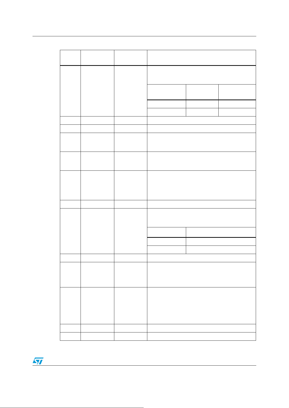
STHDLS101A Pin configuration
Table 2. Pin description (continued)
Pin
number
Name Type Function
Enable for level shifter path. 3.3 V tolerant low-voltage
single-ended input. Internal pull-down enables chip
when unconnected
25 OE_N Input
OE_N
1 High-Z High-Z
050Ω Active
26 VCC33 Power 3.3 V±10% DC supply
27 GND Power Ground
5 V DDC Clock I/O. Pulled-up by external termination
28 SCL_SINK Output
to 5 V. Connected to SCL_SOURCE through voltagelimiting integrated NMOS pass-gate
5V DDC Data I/O. Pulled-up by external termination to
29 SDA_SINK I/O
5V. Connected to SDA_SOURCE through voltagelimiting integrated NMOS pass-gate
Low-frequency, 0V to 5V (nominal) input signal. This
signal comes from the HDMI connector. Voltage high
30 HPD_SINK Input
indicates “plugged” state; voltage low indicates
“unplugged” state. HPD_SINK is pulled down by an
integrated 160KΩ pull-down resistor
31 GND Power Ground
IN_D
termination
OUT_D Outputs
Enables bias voltage to the DDC pass-gate level shifter
gates. (May be implemented as a bias voltage
connection to the DDC pass-gate themselves)
32 DDC_EN Input
DDC_EN Pass-gate
0 V Disabled
3.3 V Enabled
33 VCC33 Power 3.3 V±10% DC supply
Used for polarity control of the HPD_SOURCE output.
34 FUNCTION3 Input
When L, the HPD_SOURCE is an open-drain output
sand when H, the HPD_SOURCE is a buffered output
(O V to V
CC
)
Function pins are to enable vendor-specific features or
Vendor-specific
35 FUNCTION4
control or test
pins
test modes
For normal operation, these pins are tied to GND or
VCC33
For consistent interoperability, GND is the preferred
default connection for these signals
36 GND Power Ground
37 GND Power Ground
Doc ID 15756 Rev 1 9/24
Page 10
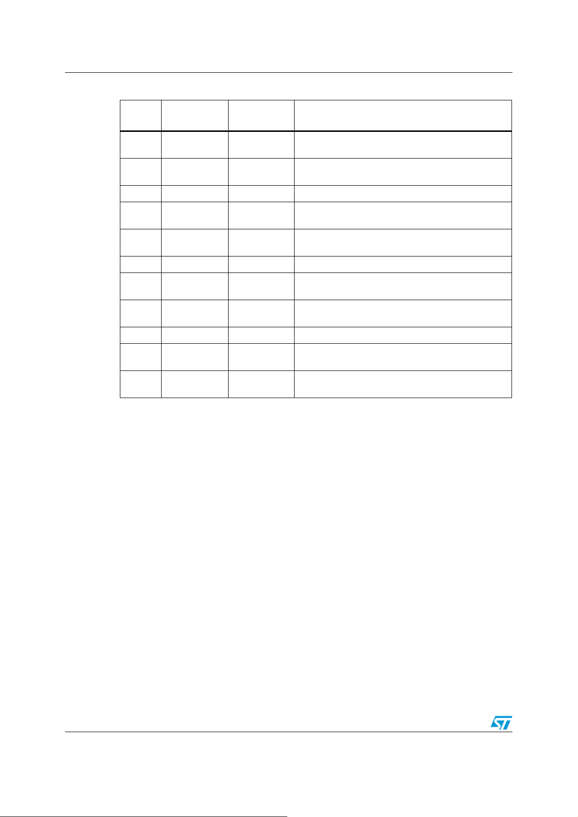
Pin configuration STHDLS101A
Table 2. Pin description (continued)
Pin
number
38 IN_D1- Input
39 IN_D1+ Input
Name Type Function
Low-swing differential input from GMCH PCIE outputs.
IN_D1- makes a differential pair with IN_D1+
Low-swing differential input from GMCH PCIE outputs.
IN_D1+ makes a differential pair with IN_D1-
40 VCC33 Power 3.3 V±10% DC supply
41 IN_D2- Input
42 IN_D2+ Input
Low-swing differential input from GMCH PCIE outputs.
IN_D2- makes a differential pair with IN_D2+
Low-swing differential input from GMCH PCIE outputs.
IN_D2+ makes a differential pair with IN_D2-
43 GND Power Ground
44 IN_D3- Input
45 IN_D3+ Input
Low-swing differential input from GMCH PCIE outputs.
IN_D3- makes a differential pair with IN_D3+
Low-swing differential input from GMCH PCIE outputs.
IN_D3+ makes a differential pair with IN_D3-
46 VCC33 Power 3.3 V±10% DC supply
47 IN_D4- Input
48 IN_D4+ Input
Low-swing differential input from GMCH PCIE outputs.
IN_D4- makes a differential pair with IN_D4+
Low-swing differential input from GMCH PCIE outputs.
IN_D4+ makes a differential pair with IN_D4-
10/24 Doc ID 15756 Rev 1
Page 11
STHDLS101A Functional description
4 Functional description
The section describes the basic functionality of the STHDLS101A device.
Power supply
The STHDLS101A is powered by a single DC power supply of 3.3 V ± 10%.
Clocking
This device does not retime any data. The device contains no state machines. No inputs or
outputs of the device are latched or clocked.
Reset
This device acts as a level shifter, reset is not required.
OE_N function
When OE_N is asserted (low level), the IN_D and OUT_D signals are fully functional. Input
termina-tion resistors are enabled and any internal bias circuits are turned on.
OE_N pin has an internal pull-down that enables the chip if left unconnected.
When OE_N is de-asserted (high level), the OUT_D outputs are in high impedance state.
The IN_D input buffers are disabled and the IN_D termination resistors are disabled.
Internal bias circuits for the differential inputs and outputs are turned off. Power consumption
of the chip is minimized.
The HPD_SINK input and HPD_SOURCE output are not affected by OE_N. The SCL and
SDA pass-gates are not affected by OE_N.
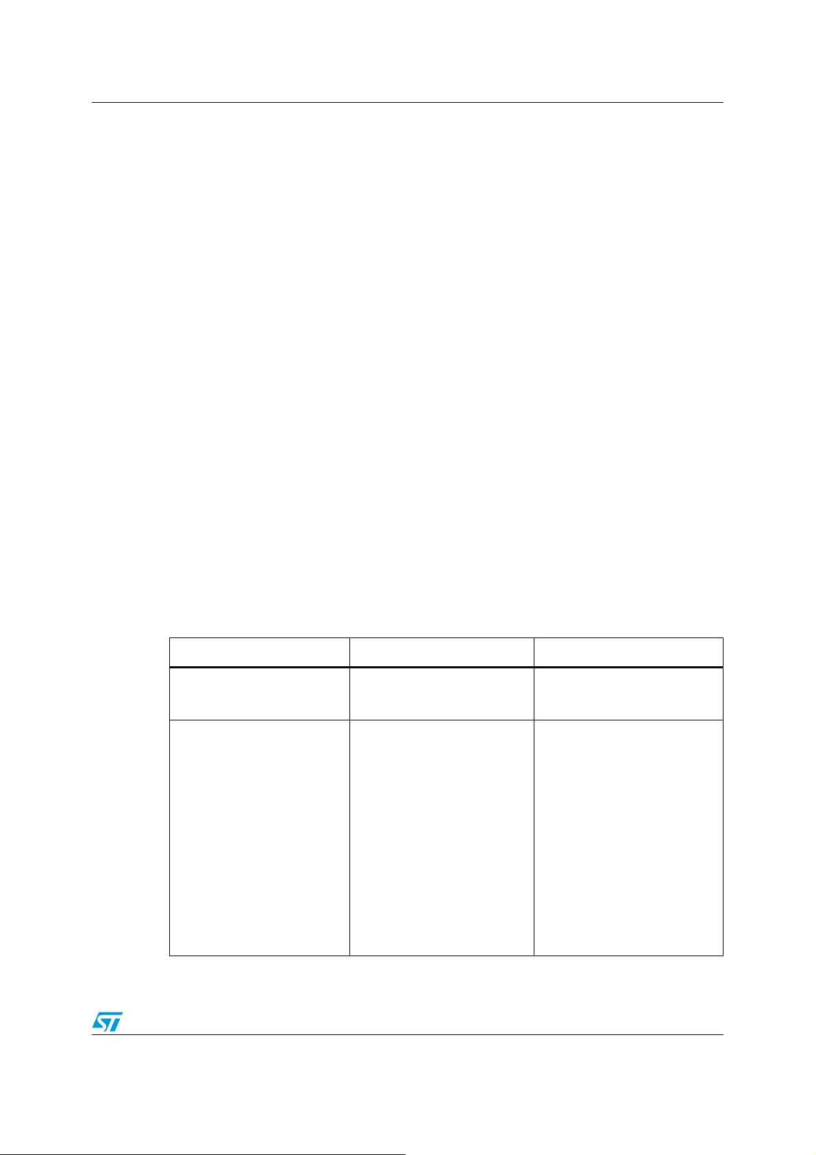
Table 3. OE_N description
OE_N Device state Comments
Asserted (low level)
or unconnected
De-asserted (high level)
Differential input buffers and
output buffers enabled. Input
impedance = 50Ù
Low-power state.
Differential input buffers and
terminations are disabled.
Differential input buffers are in
high-impedance state.
OUT_D level shifting outputs are
disabled. OUT_D level shifting
outputs are in a high-impedance
state.
Internal bias currents are turned
off.
Normal functioning state for IN_D
to OUT_D level shifting function.
Intended for lowest power
condition when:
• No display is plugged in or
• The level shifted data path is
disabled
HPD_SINK input and
HPD_SOURCE output are not
affected by OE_N.
SCL_SOURCE, SCL_SINK,
SDA_SOURCE and SDA_SINK
signals and functions are not
affected by OE_N.
Doc ID 15756 Rev 1 11/24
Page 12
Functional description STHDLS101A
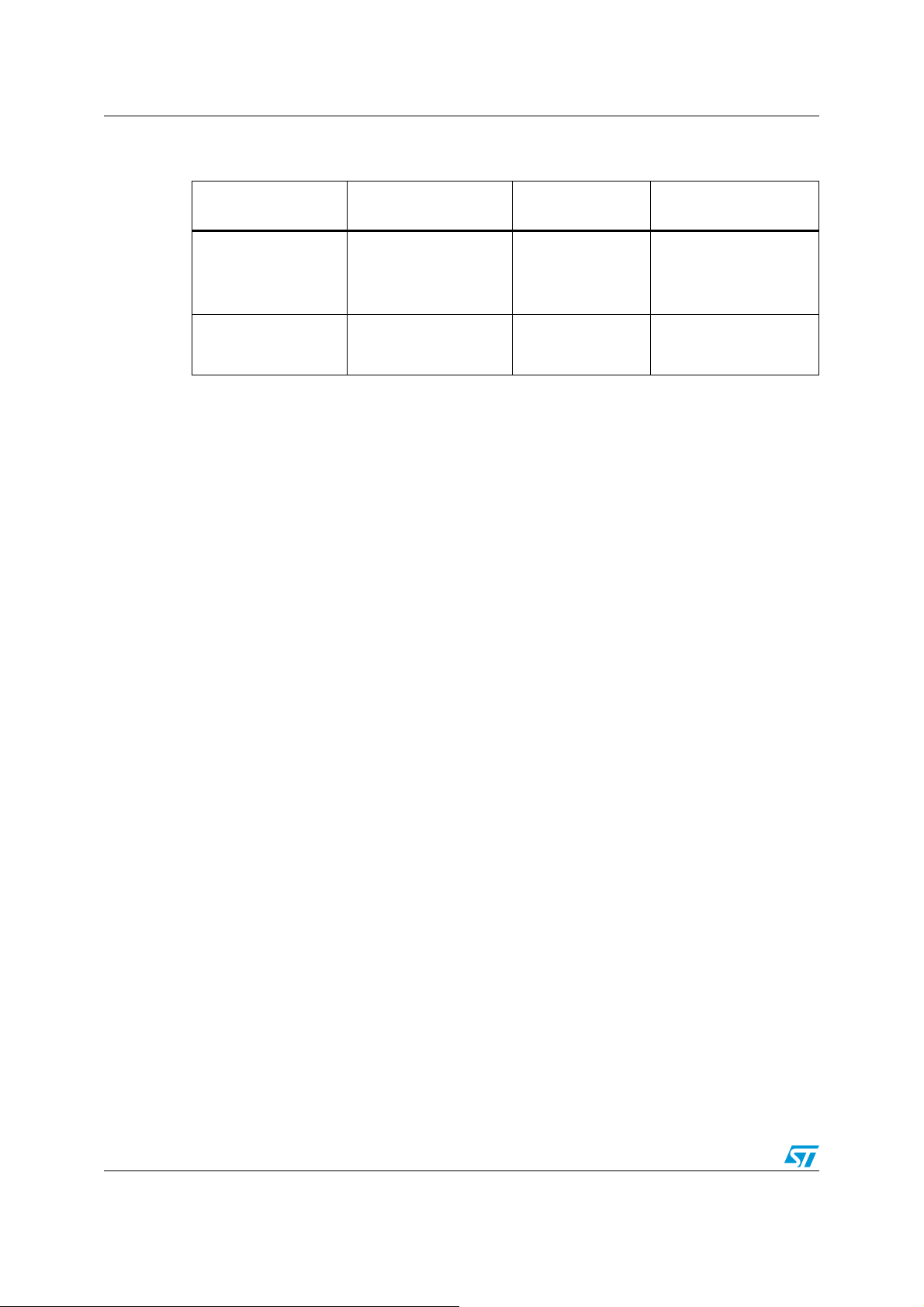
Table 4. OE_N function
OE_N IN_Dx
De-asserted
(high level)
Asserted or
unconnected
50 Ω termination Enabled
(low level)
OUT_Dx
(TMDS outputs)
High-Z High-Z
Notes
Device disabled.
Low power state.
Internal bias currents are
disabled.
Level shifting mode
enabled.
12/24 Doc ID 15756 Rev 1
Page 13
STHDLS101A Maximum ratings
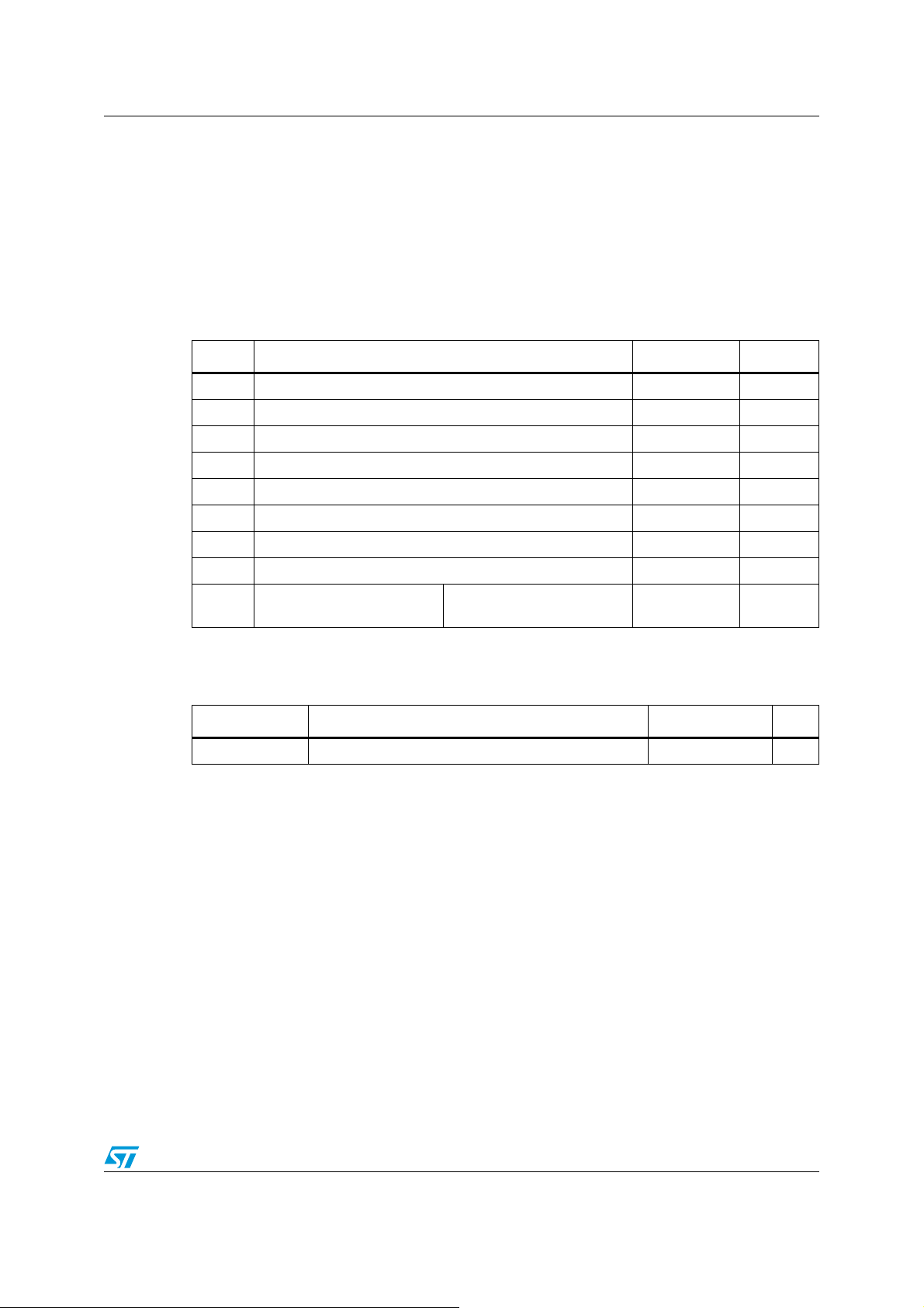
5 Maximum ratings
Stressing the device above the rating listed in the “Absolute maximum ratings” table may
cause permanent damage to the device. These are stress ratings only and operation of the
device at these or any other conditions above those indicated in the Operating sections of
this specification is not implied. Exposure to Absolute maximum rating conditions for
extended periods may affect device reliability.
Table 5. Absolute maximum ratings
Symbol Parameter Value Unit
V
Supply voltage to ground potential -0.5 to +4.0 V
CC
DC input voltage (TMDS and PCIe ports) -0.5 to +4.0 V
V
I
Control pins -0.5 to +4.0 V
SDA_SINK, SCL_SINK, HPD_SINK pins -0.5 to +6 V
DC output current 120 mA
I
O
P
Power dissipation 1 W
D
T
V
Storage temperature -65 to +150 °C
STG
Lead temperature (10 sec) 300 °C
T
L
Electrostatic discharge
ESD
voltage on IOs
(1)
Human body model ±6 kV
1. In accordance with the MIL standard 883 method 3015
Table 6. Thermal data
Symbol Parameter QFN48 Unit
θ
JA
Junction-ambient thermal coefficient 48 °C/W
Doc ID 15756 Rev 1 13/24
Page 14
Maximum ratings STHDLS101A
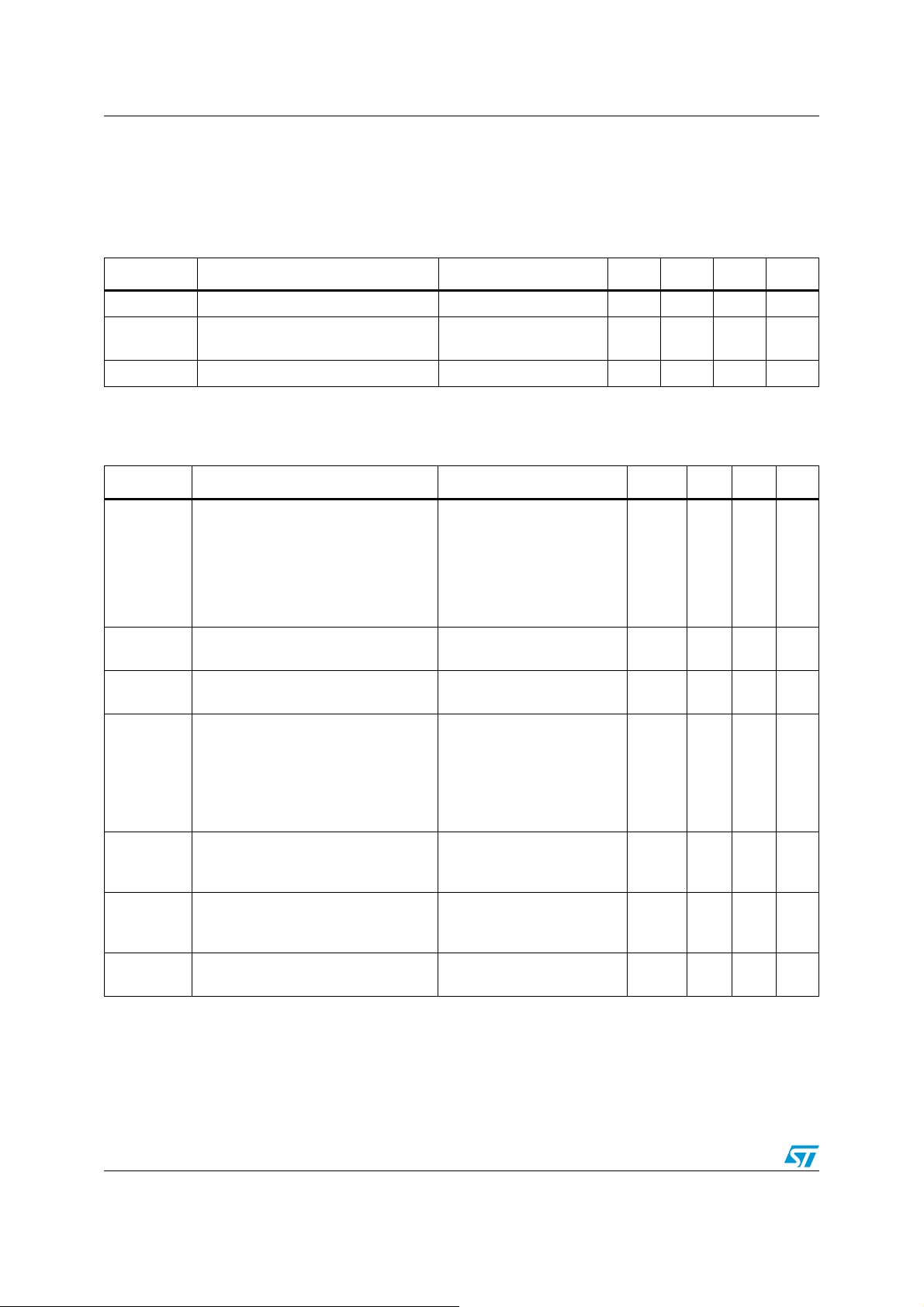
5.1 Recommended operating conditions
5.1.1 Power supply and temperature range
Table 7. Power supply and temperature range
Symbol Parameter Comments Min Typ Max Unit
V
CC33
I
CC
3.3 V power supply 3.0 3.3 3.6 V
Maximum power supply current
Total current from V
3.3 V power supply
CC
−−120 mA
T Operating temperature range -40 − 85
5.1.2 Differential inputs (IN_D signals)
Table 8. Differential input characteristics for IN_D signals
Symbol Parameter Comments Min Typ Max Unit
Tbit Unit interval
V
RX-DIFFp-p
T
RX-EYE
V
CM-AC-pp
Z
RX-DC
V
RX-Bias
Z
RX-HIGH-Z
Differential input peak to peak voltage
Minimum eye width at IN_D input pair
AC peak common mode input voltage
DC single-ended input impedance
RX input termination voltage
Single-ended input resistance for
IN_Dx when inputs are in high-Z state
Tbit is determined by the
display mode. Nominal bit
rate ranges from 250 Mbps
to 2.5 Gbps per lane.
Nominal Tbit at
2.5 Gbps = 400 ps. 360 ps =
400 ps – 10%
V
RX-DIFFp-p
|. Applies to IN_D signals.
D-
=2*|V
RX-D+
- V
RX-
The level shifter may add a
maximum of 0.02UI jitter
VCM-AC-pp=|VRX-D+ +
VRX-D-|/2 – VRX-CM-DC.
VRX-CM-DC=DC(avg) of
|VRX-D+ + VRX-D-|/2
VCM-AC-pp includes all
frequencies above 30 kHz.
Applies to IN_D+ as well as
IN_D- pins (50 Ω ± 20%
tolerance)
Intended to limit power-up
stress on chipset’s PCIE
output buffers
Differential inputs must be in
a high impedance state
360 −−ps
0.2
− 1.2 V
0.8 −−Tbit
−−100 mV
40 50 60 Ω
0 − 2V
100
−−KΩ
o
C
14/24 Doc ID 15756 Rev 1
Page 15
STHDLS101A Maximum ratings
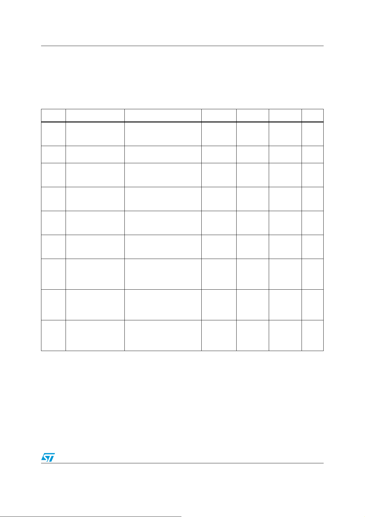
5.2 TMDS outputs (OUT_D signals)
The level shifter’s TMDS outputs are required to meet the HDMI 1.3 specifications. The
HDMI 1.3 specification is assumed to be the correct reference in instances where this
document conflicts with the HDMI 1.3 specification.
Table 9. Differential output characteristics for TMDS OUT_D signals
Symbol Parameter Comments Min Typ Max Unit
is the DC termination
AV
V
V
V
SWING
I
OFF
T
T
T
SKEW-
INTRA
Single-ended high
H
level output voltage
Single-ended low level
L
output voltage
Single-ended output
swing voltage
Single-ended current
in high-Z state
Rise time
R
Fall time
F
Intra-pair differential
skew
CC
voltage in the HDMI or DVI
sink. AV
is nominally 3.3 V
CC
The open-drain output pulls
down form AV
CC
Swing down from TMDS
termination voltage
(3.3 V ±10%)
Measured with TMDS outputs
pulled up to AV
max (3.6 V)
CC
through 50 Ω resistors
Maximum rise/fall time at
2.7 Gbps = 148ps. 125ps =
148 – 15%
Maximum rise/fall time at
2.7 Gbps = 148 ps.
125ps = 148 – 15%
This differential skew budget
is in addition to the skew
presented between D+ and Dpaired input pins.
AVCC-10 mV AV
AVCC-
600 mV
AVCC-
500 mV
CC
AVCC+10 m
V
AVCC-
400 mV
400 mV 500 mV 600 mV V
−−10 µA
125 ps − 0.4 Tbit ps
125 ps − 0.4 Tbit ps
−−10 ps
V
V
This lane to lane skew budget
T
SKEW-
INTER
Inter-pair lane to lane
output skew
is in addition to the skew
between differential input
−−250 ps
pairs.
Jitter budget for TMDS
T
Jitter added to TMDS
JIT
signals
signals as they pass through
the level shifter.
−−7.4 ps
7.4 ps = 0.02 Tbit at 2.7 Gbps
Doc ID 15756 Rev 1 15/24
Page 16
Maximum ratings STHDLS101A
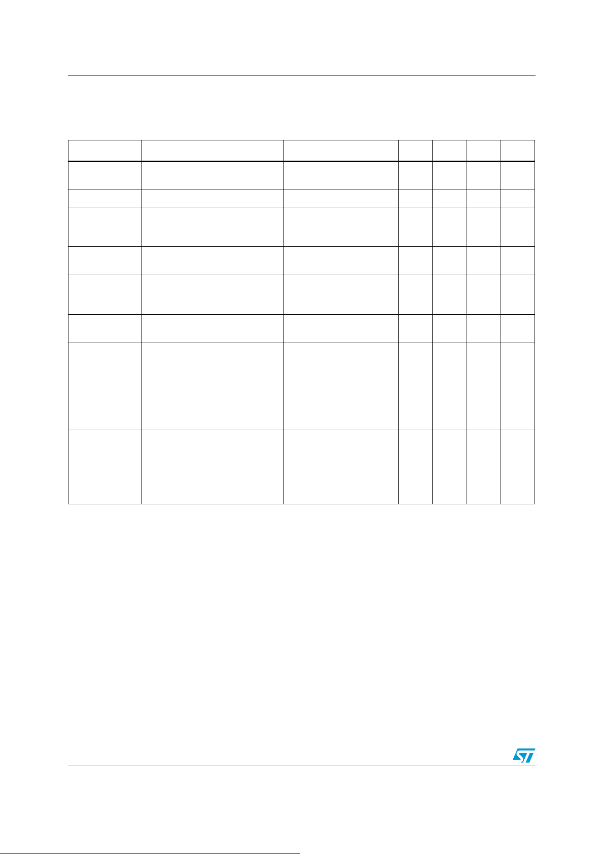
5.3 HPD input and output characteristics
Table 10. HPD_SINK input and HPS_SOURCE output
Symbol Parameter Comment Min Typ Max Unit
V
IH-HPD_SINK
V
IL-HPD_SINK
I
IN-HPD_SINK
V
OL-
HPD_SOURCE
V
OH-
HPD_SOURCE
(INV)
V
OL-
HPD_SOURCE
T
HPD
T
RF-HPD
HPD_SINK input high level
Low speed input changes
state on cable plug/unplug
25.05.3V
HPD_SINK input low level 0 − 0.8 V
Measured with HPD_SINK
HPD_SINK input leakage current
HPD_SOURCE output low level
when FUNCTION3 = H
HPD_SOURCE output high level
when FUNCTION3 = L
HPD_SOURCE output low level
when FUNCTION3 = H
at V
HPD
V
CC
V
CC
I
OL
V
CC
IH-HPD
max and V
IL-
−−50 µA
min
= 3.3 V ±10% 2.5 − V
= 3.3 V ±10%
=1mA
0 − 0.2 V
= 3.3 V ±10% 0 − 0.2 V
CC
Time from HPD_SINK
changing state to
HPD_SINK to HPD_SOURCE
propagation delay
HPD_SOURCE changing
state. Includes
HPD_SOURCE rise/fall
−−200 ns
time
=10 pF
C
L
Time required to transition
HPD_SOURCE rise/fall time
from V
OH-HPD_SOURCE
V
OL-HPD_SOURCE
V
OL-HPD_SOURCE
HPD_SOURCE
to
or from
to V
OH-
1
− 20 ns
CL=10 pF
V
16/24 Doc ID 15756 Rev 1
Page 17
STHDLS101A Maximum ratings
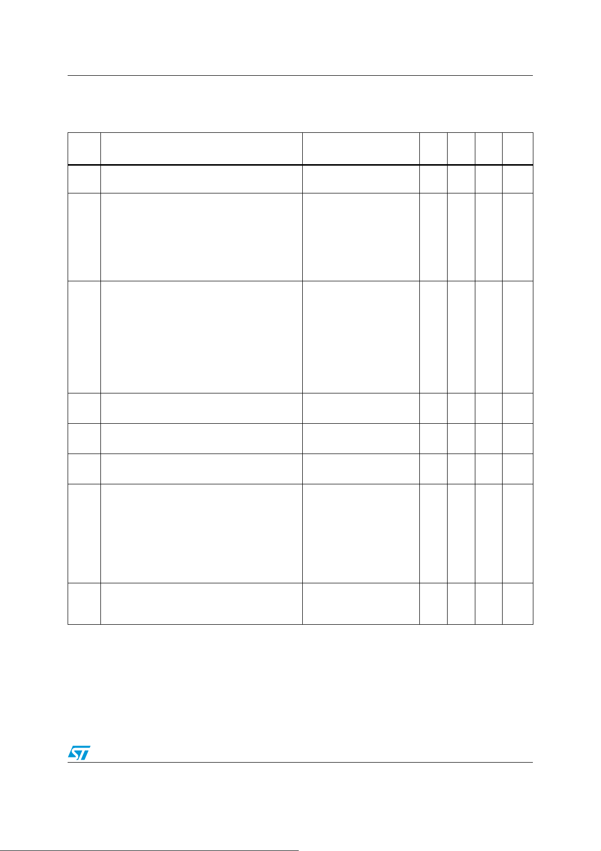
5.4 DDC input and output chatacteristics
Table 11. SDA_SOURCE, SCL_SOURCE and SDA_SINK, SCL_SINK characteristics
Symb
ol
V
I
Parameter Comment Min Typ Max Unit
Input voltage on SDA_SINK, SCL_SINK pins
Voltage on the DDC pins on
connector end
0
− 5.5 V
VCC=3.3V
=0.1VDD to 0.9 VDD to
V
I
Input leakage current on SDA_SINK, SCL_SINK
I
LKG
pins
isolated DDC inputs
= external pull-up
V
DD
resistor voltage on
-10
− 10 µA
SDA_SINK and SCL_SINK
inputs (maximum of 5.5 V)
=0.0V
V
CC
= 0.1 VDD to 0.9 VDD to
V
I
DDC sink inputs
= external pull-up
V
Power-down leakage current on SDA_SINK,
I
OFF
SCL_SINK pins
DD
resistor voltage on
SDA_SINK and SCL_SINK
-10
− 10 µA
inputs (maximum of 5.5 V)
SDA_SOURCE,
SCL_SOURCE = 0.0 V
=1 V, 100 KHz
Input/output capacitance
C
I/O
(switch off)
Input/output capacitance
C
I/O
(switch on)
R
Switch resistance
ON
V
I(pp)
=3.3 V, T=25C
V
CC
=1 V, 100KHz
V
I(pp)
= 3.3 V, T= 25 ° C
V
CC
I
=3 mA, VO=0.4V
O
=3.3V
V
CC
− 5 − pF
−−10 pF
− 27 40 Ω
Time from DDC_SINK
changing state to
DDC_SOURCE changing
DDC_SINK to DDC_SOURCE propagation delay
T
PD
state while the pass gate is
enabled.
=10 pF
C
L
=1.5 K (min), 2.0 K
R
PU
− 815ns
(max)
Switch time from DDC_EN to the valid state on
T
SX
DDC_SOURCE
CL=10pF
RPU= 1.5 K (min), 2.0 K
(max)
− 815ns
Doc ID 15756 Rev 1 17/24
Page 18
Maximum ratings STHDLS101A
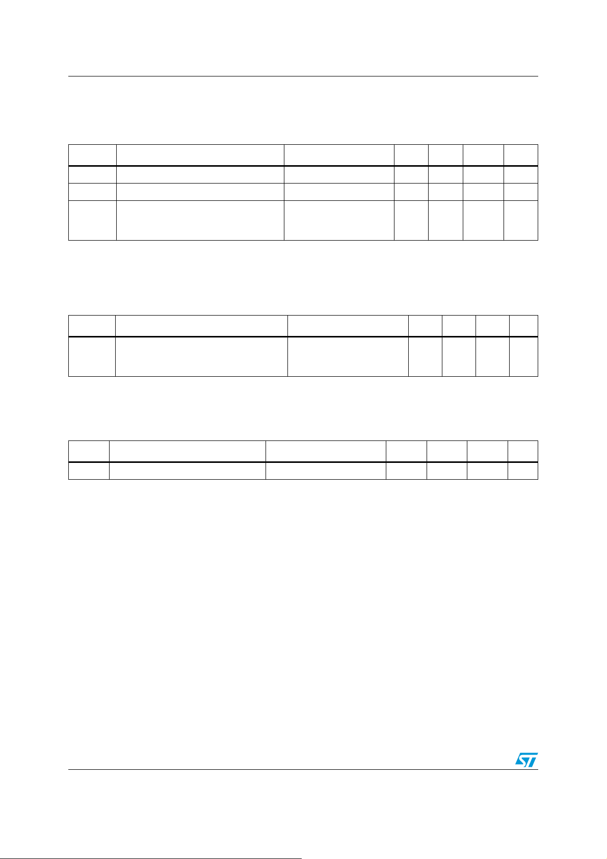
5.5 OE_ input characteristics
Table 12. OE_N input characteristics
Symbol Parameter Comment Min Typ Max Unit
V
IH-OE_N
V
IL-OE_N
Input high level 2 − VCC33 V
Input low level 0 − 0.8 V
Measured with OE_N at
I
IN-OE_N
Input leakage current
VIH-OE_N max and VIL-
−−200 µA
OE_N min
5.6 HPD input resistor
Table 13. HDP input resistor
Symbol Parameter Comment Min Typ Max Unit
Guarantees HPD_SINK is
R
HPD
HPD_SINK input pull-down resistor
LOW when no display is
plugged in
130 K 160 K 190 K Ω
5.7 ESD performance
Table 14. ESD performance
Symbol Parameter Test condition Min Typ Max Unit
ESD MIL STD 883 method 3015 (all pins) Human Body Model (HBM) -6
18/24 Doc ID 15756 Rev 1
− +6 kV
Page 19

STHDLS101A Application information
6 Application information
6.1 Power supply sequencing
Proper power-supply sequencing is advised for all CMOS devices. It is
recommended to always apply V
or control pins.
6.2 Supply bypassing
Bypass each of the VCC pins with 0.1 µF and 1nF capacitors in parallel as close to the
device as possible, with the smaller-valued capacitor as close to the V
as possible.
6.3 Differential traces
The high-speed inputs and TMDS outputs are the most critical parts for the device. There
are several considerations to minimize discontinuities on these transmission lines between
the connectors and the device.
before applying any signals to the input/output
CC
pin of the device
CC
(a) Maintain 100 Ω differential transmission line impedance into and out of the device.
(b) Keep an uninterrupted ground plane below the high-speed I/Os.
(c) Keep the ground-path vias to the device as close as possible to allow the shortest return
current path.
(d) Layout of the TMDS differential outputs should be with the shortest stubs from the
connectors.
Output trace characteristics affect the performance of the STHDLS101A. Use controlled
impedance traces to match trace impedance to both the transmission medium impedance
and termination resistor. Run the differential traces close together to minimize the effects of
the noise. Reduce skew by matching the electrical length of the traces. Avoid discontinuities
in the differential trace layout. Avoid 90 degree turns and minimize the number of vias to
further prevent impedance discontinuities.
Doc ID 15756 Rev 1 19/24
Page 20
Package mechanical data STHDLS101A
7 Package mechanical data
In order to meet environmental requirements, ST offers these devices in different grades of
ECOPACK
specifications, grade definitions and product status are available at: www.st.com.
ECOPACK
®
packages, depending on their level of environmental compliance. ECOPACK®
®
is an ST trademark.
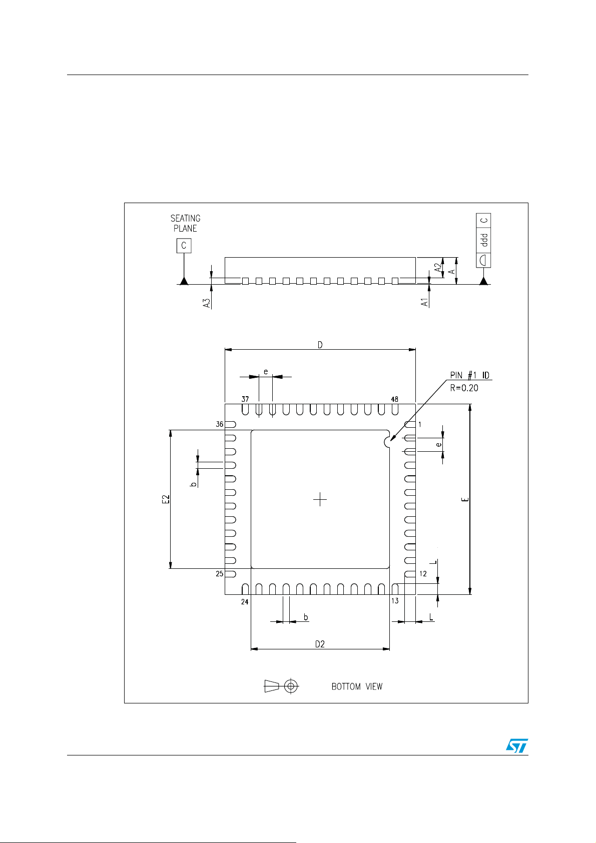
Figure 6. Package outline for QFN48 (7x7x 1 mm) - 0.5 mm pitch
20/24 Doc ID 15756 Rev 1
Page 21
STHDLS101A Package mechanical data
Table 15. Package mechanical data for QFN48 (7 x 7 x 1 mm) - 0.5 mm pitch
Symbol Min Typ Max Min Typ Max
A 0.80 0.90 1.00 0.80 0.85 1.00
A1 − 0.02 0.05 − 0.01 0.05
A2
A3 − 0.25 −−0.20 −
b 0.18 0.23 0.30 0.18 0.23 0.30
D 6.85 7.00 7.15 6.90 7.00 7.10
D2 2.25 4.70 5.25 SEE EXPOSED PAD VARIATIONS
E 6.85 7.00 7.15 6.90 7.00 7.10
E2 2.25 4.70 5.25 SEE EXPOSED PAD VARIATIONS
e 0.45 0.50 0.55 0.45 0.50 0.55
L 0.30 0.40 0.50 0.30 0.40 0.50
ddd
− 0.65 1.00 − 0.65 −
−−0.08 −−0.08
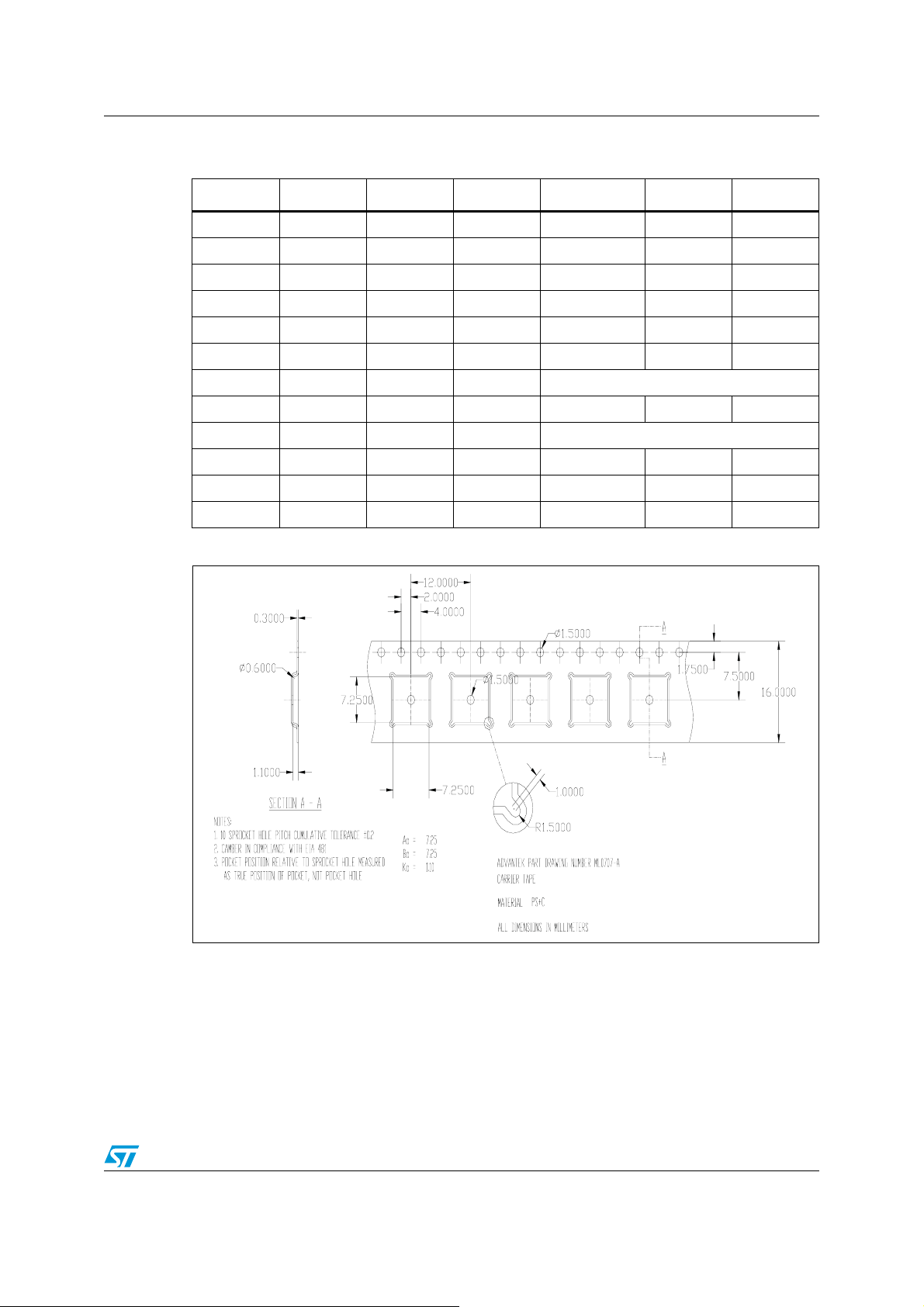
Figure 7. Tape information for QFN48 (7 x 7 x 1 mm) - 0.5 mm pitch
Doc ID 15756 Rev 1 21/24
Page 22
Package mechanical data STHDLS101A
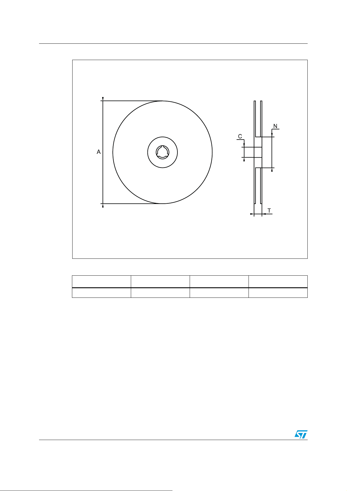
Figure 8. Reel information for QFN48 (7 x 7 x 1 mm) - 0.5 mm pitch
0084694_J
Table 16. Reel mechanical data (dimensions in mm)
ACNT
330.2 13
±0.25 100 16.4
22/24 Doc ID 15756 Rev 1
Page 23
STHDLS101A Revision history
8 Revision history
Table 17. Document revision history
Date Revision Changes
22-Jun-2009 1 Initial release.
Doc ID 15756 Rev 1 23/24
Page 24

STHDLS101A
Please Read Carefully:
Information in this document is provided solely in connection with ST products. STMicroelectronics NV and its subsidiaries (“ST”) reserve the
right to make changes, corrections, modifications or improvements, to this document, and the products and services described herein at any
time, without notice.
All ST products are sold pursuant to ST’s terms and conditions of sale.
Purchasers are solely responsible for the choice, selection and use of the ST products and services described herein, and ST assumes no
liability whatsoever relating to the choice, selection or use of the ST products and services described herein.
No license, express or implied, by estoppel or otherwise, to any intellectual property rights is granted under this document. If any part of this
document refers to any third party products or services it shall not be deemed a license grant by ST for the use of such third party products
or services, or any intellectual property contained therein or considered as a warranty covering the use in any manner whatsoever of such
third party products or services or any intellectual property contained therein.
UNLESS OTHERWISE SET FORTH IN ST’S TERMS AND CONDITIONS OF SALE ST DISCLAIMS ANY EXPRESS OR IMPLIED
WARRANTY WITH RESPECT TO THE USE AND/OR SALE OF ST PRODUCTS INCLUDING WITHOUT LIMITATION IMPLIED
WARRANTIES OF MERCHANTABILITY, FITNESS FOR A PARTICULAR PURPOSE (AND THEIR EQUIVALENTS UNDER THE LAWS
OF ANY JURISDICTION), OR INFRINGEMENT OF ANY PATENT, COPYRIGHT OR OTHER INTELLECTUAL PROPERTY RIGHT.
UNLESS EXPRESSLY APPROVED IN WRITING BY AN AUTHORIZED ST REPRESENTATIVE, ST PRODUCTS ARE NOT
RECOMMENDED, AUTHORIZED OR WARRANTED FOR USE IN MILITARY, AIR CRAFT, SPACE, LIFE SAVING, OR LIFE SUSTAINING
APPLICATIONS, NOR IN PRODUCTS OR SYSTEMS WHERE FAILURE OR MALFUNCTION MAY RESULT IN PERSONAL INJURY,
DEATH, OR SEVERE PROPERTY OR ENVIRONMENTAL DAMAGE. ST PRODUCTS WHICH ARE NOT SPECIFIED AS "AUTOMOTIVE
GRADE" MAY ONLY BE USED IN AUTOMOTIVE APPLICATIONS AT USER’S OWN RISK.
Resale of ST products with provisions different from the statements and/or technical features set forth in this document shall immediately void
any warranty granted by ST for the ST product or service described herein and shall not create or extend in any manner whatsoever, any
liability of ST.
ST and the ST logo are trademarks or registered trademarks of ST in various countries.
Information in this document supersedes and replaces all information previously supplied.
The ST logo is a registered trademark of STMicroelectronics. All other names are the property of their respective owners.
© 2009 STMicroelectronics - All rights reserved
STMicroelectronics group of companies
Australia - Belgium - Brazil - Canada - China - Czech Republic - Finland - France - Germany - Hong Kong - India - Israel - Italy - Japan -
Malaysia - Malta - Morocco - Philippines - Singapore - Spain - Sweden - Switzerland - United Kingdom - United States of America
www.st.com
24/24 Doc ID 15756 Rev 1
 Loading...