

Page 1
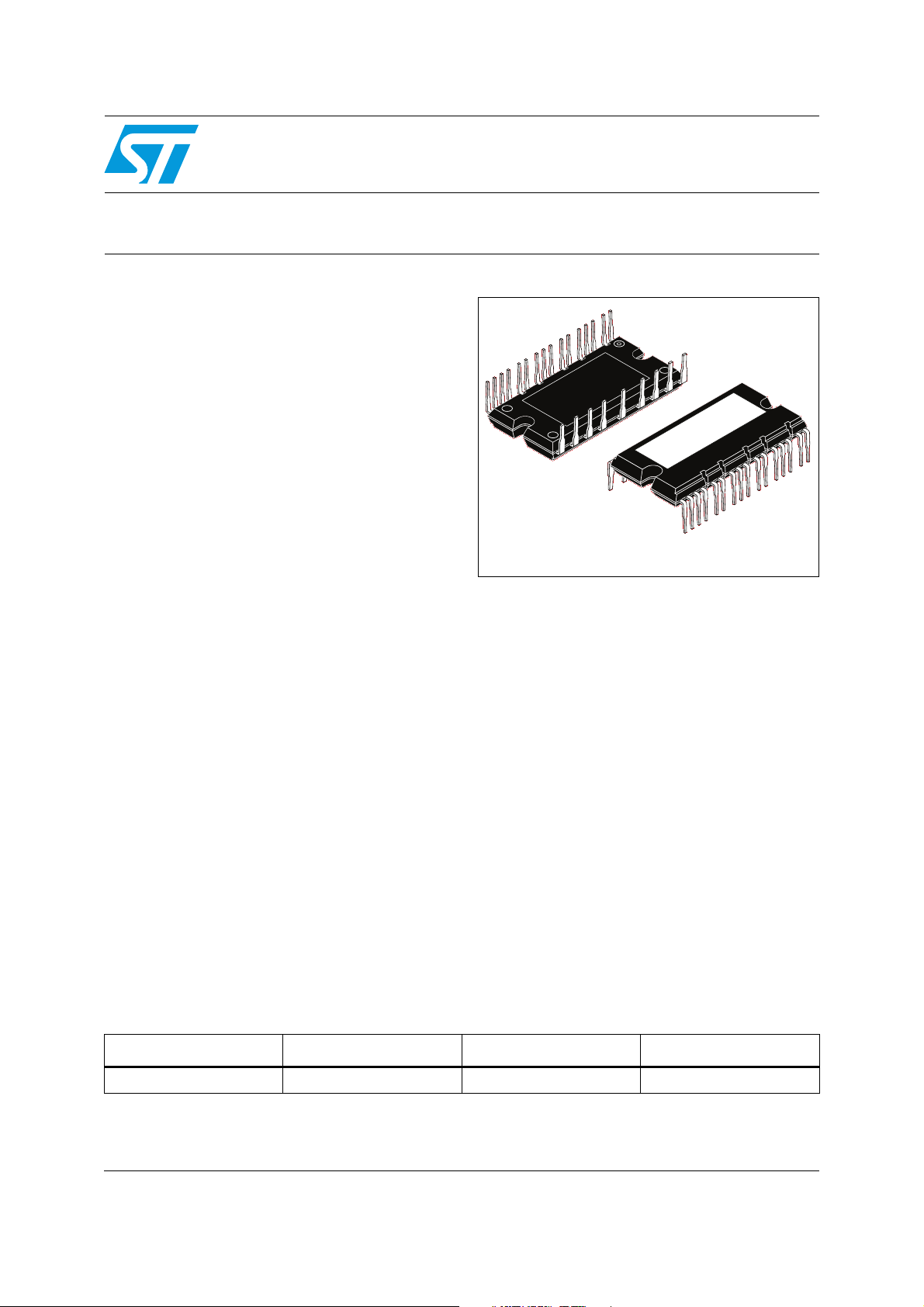
SLLIMM™ (small low-loss intelligent molded module)
IPM, 3-phase inverter - 14 A, 600 V short-circuit rugged IGBT
Features
■ IPM 14 A, 600 V 3-phase IGBT inverter bridge
including control ICs for gate driving and freewheeling diodes
■ Short-circuit rugged IGBTs
■ V
■ 3.3 V, 5 V, 15 V CMOS/TTL inputs
comparators with hysteresis and pull down /
pull up resistors
■ Undervoltage lockout
■ Internal bootstrap diode
■ Interlocking function
■ Shutdown function
■ Comparator for fault protection against
overtemperature and overcurrent
■ DBC substrate leading to low thermal
resistance
■ Isolation rating of 2500 Vrms/min
Applications
■ 3-phase inverters for motor drives
■ Home appliances, such as washing machines,
refrigerators, air conditioners and sewing
machines
negative temperature coefficient
CE(sat)
STGIPS14K60
SDIP-25L
Description
This intelligent power module provides a
compact, high performance AC motor drive in a
simple, rugged design. Combining ST proprietary
control ICs with the most advanced short-circuitrugged IGBT system technology, this device is
ideal for 3-phase inverters in applications such as
home appliances and air conditioners. SLLIMM™
is a trademark of STMicroelectronics.
Table 1. Device summary
Order code Marking Package Packaging
STGIPS14K60 GIPS14K60 SDIP-25L Tube
November 2011 Doc ID 15927 Rev 6 1/20
www.st.com
20
Page 2

Contents STGIPS14K60
Contents
1 Internal block diagram and pin configuration . . . . . . . . . . . . . . . . . . . . 3
2 Electrical ratings . . . . . . . . . . . . . . . . . . . . . . . . . . . . . . . . . . . . . . . . . . . . 5
2.1 Absolute maximum ratings . . . . . . . . . . . . . . . . . . . . . . . . . . . . . . . . . . . . . 5
2.2 Thermal data . . . . . . . . . . . . . . . . . . . . . . . . . . . . . . . . . . . . . . . . . . . . . . . 6
3 Electrical characteristics . . . . . . . . . . . . . . . . . . . . . . . . . . . . . . . . . . . . . 7
3.1 Control part . . . . . . . . . . . . . . . . . . . . . . . . . . . . . . . . . . . . . . . . . . . . . . . . 9
3.2 Waveforms definitions . . . . . . . . . . . . . . . . . . . . . . . . . . . . . . . . . . . . . . . 12
4 Smart shutdown function . . . . . . . . . . . . . . . . . . . . . . . . . . . . . . . . . . . . 13
5 Applications information . . . . . . . . . . . . . . . . . . . . . . . . . . . . . . . . . . . . 14
5.1 Recommendations . . . . . . . . . . . . . . . . . . . . . . . . . . . . . . . . . . . . . . . . . . 15
6 Package mechanical data . . . . . . . . . . . . . . . . . . . . . . . . . . . . . . . . . . . . 16
7 Revision history . . . . . . . . . . . . . . . . . . . . . . . . . . . . . . . . . . . . . . . . . . . 19
2/20 Doc ID 15927 Rev 6
Page 3
STGIPS14K60 Internal block diagram and pin configuration
P
P
P
U
V
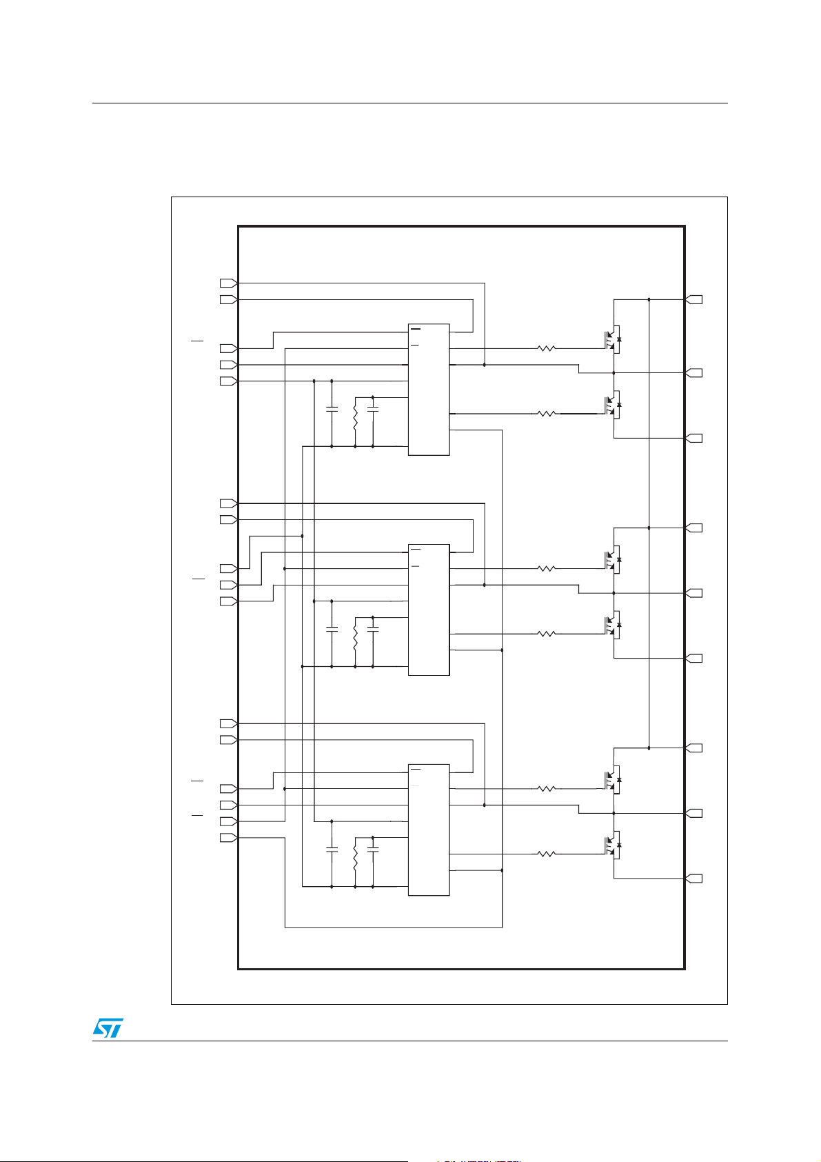
1 Internal block diagram and pin configuration
Figure 1. Internal block diagram
Pin 1
OUT U
VBOOT U
LIN-U
HIN-U
VCC
OUT V
VBOOT V
GND
LIN-V
HIN-V
LIN
SD/O D
HIN
VCC
DT
GND
LIN
SD/O D
HIN
VCC
DT
GND
Vboot
HVG
OUT
LVG
CP+
Vboot
HVG
OUT
LVG
CP+
Pin 25
NU
NV
OUT W
VBOOT W
LIN
Vboot
LIN-W
HIN-W
SD/OD
CIN
Pin 16
SD/OD
HIN
VCC
DT
GND
HVG
OUT
LVG
CP+
W
NW
Pin 17
AM05002v1
Doc ID 15927 Rev 6 3/20
Page 4
Internal block diagram and pin configuration STGIPS14K60
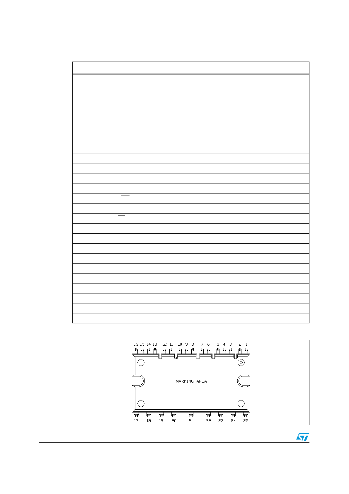
Table 2. Pin description
Pin n° Symbol Description
1OUT
2V
3LIN
4HIN
5V
6OUT
7V
U
boot U
U
U
CC
V
boot V
High side reference output for U phase
Bootstrap voltage for U phase
Low side logic input for U phase
High side logic input for U phase
Low voltage power supply
High side reference output for V phase
Bootstrap voltage for V phase
8 GND Ground
9LIN
10 HIN
11 OUT
12 V
13 LIN
14 HIN
15 SD
V
V
W
boot W
W
W
/ OD Shut down logic input (active low) / open drain (comparator output)
Low side logic input for V phase
High side logic input for V phase
High side reference output for W phase
Bootstrap voltage for W phase
Low side logic input for W phase
High side logic input for W phase
16 CIN Comparator input
17 N
W
Negative DC input for W phase
18 W W phase output
19 P Positive DC input
20 N
V
Negative DC input for V phase
21 V V phase output
22 P Positive DC input
23 N
U
Negative DC input for U phase
24 U U phase output
25 P Positive DC input
Figure 2. Pin layout (bottom view)
4/20 Doc ID 15927 Rev 6
Page 5
STGIPS14K60 Electrical ratings
2 Electrical ratings
2.1 Absolute maximum ratings
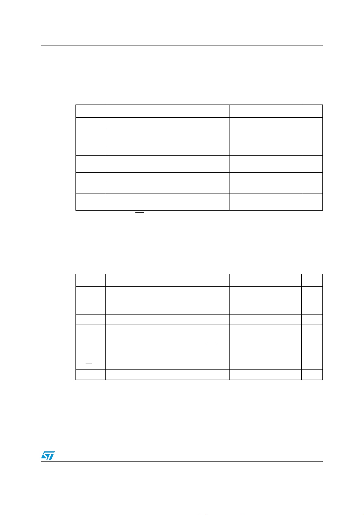
Table 3. Inverter part
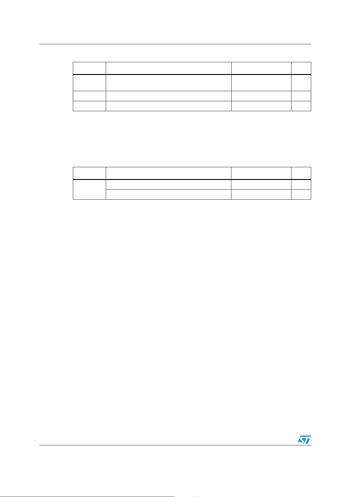
Symbol Parameter Value Unit
V
V
PN(surge)
V
CES
± I
C
± I
CP
P
TOT
t
scw
1. Applied between HIN
Supply voltage applied between P - NU, NV, N
PN
W
Supply voltage (surge) applied between P - NU,
NV, N
W
Each IGBT collector emitter voltage (V
Each IGBT continuous collector current
(2)
(1)
= 0)
IN
at TC = 25°C
(3)
Each IGBT pulsed collector current 30 A
450 V
500 V
600 V
14 A
Each IGBT total dissipation at TC = 25°C 42 W
Short circuit withstand time, VCE = 0.5 V
TJ = 125 °C, VCC = V
, LINi and GND for i = U, V, W
i
= 15 V, V
boot
IN
(1)
(BR)CES
= 0 ÷ 5 V
5µs
2. Calculated according to the iterative formula:
ICTC()
-------------------------------------------------------------------------------------------------------=
R
thj c–
T
V
CE sat()max()Tjmax()ICTC
–
jmax()TC
(),()×
3. Pulse width limited by max junction temperature
Table 4. Control part
Symbol Parameter Value Unit
V
V
V
OUT
V
V
CC
CIN
boot
IN
Output voltage applied between
OUT
OUT
U,
OUTW - GND
V,
Low voltage power supply -0.3 to +21 V
Comparator input voltage -0.3 to VCC +0.3 V
Bootstrap voltage applied between
- OUTi for i = U, V, W
V
boot i
Logic input voltage applied between HIN, LIN and
GND
V
- 21 to V
boot
boot
-0.3 to 620 V
-0.3 to 15 V
+ 0.3 V
V
SD/OD
dV
OUT
Open drain voltage -0.3 to 15 V
/dt Allowed output slew rate 50 V/ns
Doc ID 15927 Rev 6 5/20
Page 6
Electrical ratings STGIPS14K60
Table 5. Total system
Symbol Parameter Value Unit
V
ISO
(1)
T
j
T
C
1. The maximum junction temperature rating of the power chips integrated within the SDIP module is 150°C
(@TC ≤ 100°C). To ensure safe operation of the SDIP module, the average junction temperature should be
limited to T
Isolation withstand voltage applied between each
pin and heatsink plate (AC voltage, t = 60 sec.)
Operating junction temperature -40 to 150 °C
Module case operation temperature -40 to 125 °C
≤ 125°C (@TC ≤ 100°C).
j(avg)
2.2 Thermal data
Table 6. Thermal data
Symbol Parameter Value Unit
R
thJC
Thermal resistance junction-case single IGBT 3 °C/W
Thermal resistance junction-case single diode 5.5 °C/W
2500 V
6/20 Doc ID 15927 Rev 6
Page 7
STGIPS14K60 Electrical characteristics
3 Electrical characteristics
TJ = 25 °C unless otherwise specified.
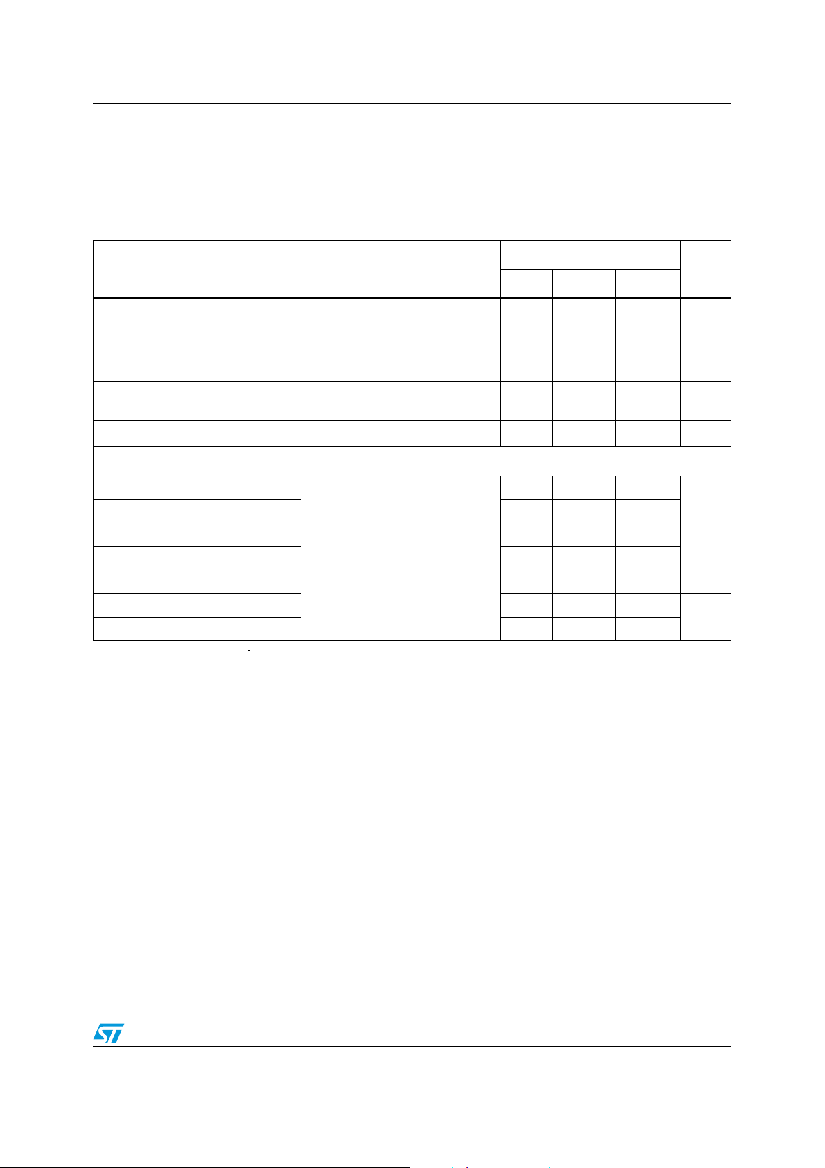
Table 7. Inverter part
Val ue
Symbol Parameter Test conditions
V
CE(sat)
I
CES
V
Collector-emitter
saturation voltage
Collector-cut off current
(1)
(V
= 0 “logic state”)
IN
Diode forward voltage V
F
VCC = V
= 7 A
I
C
V
CC
= 7 A, TJ = 125 °C
I
C
V
CE
(1)
IN
= 15 V, V
boot
= V
= 15 V, V
boot
= 600 V, V
CC
= V
IN
IN
Boot
= 0 “logic state”, IC = 7 A - 2.1 V
Inductive load switching time and energy
Min. Typ. Max.
(1)
= 0 ÷ 5 V,
(1)
= 0 ÷ 5 V,
-2.12.5
-1.8
= 15 V - 150 µA
Unit
V
t
t
c(on)
t
t
c(off)
E
E
1. Applied between HIN
Note: t
Turn-on time
on
Crossover time (on) - 130
Turn-off time - 320
off
Crossover time (off) - 110
Reverse recovery time - 130
t
rr
Turn-on switching losses - 150
on
Turn-off switching losses - 90
off
and t
ON
the switching time of IGBT itself under the internally given gate driving condition.
- 270
V
= 300 V,
DD
= V
V
CC
(1)
V
IN
= 15 V,
boot
= 0 ÷ 5 V,
IC = 7 A
(see Figure 5)
, LINi and GND for i = U, V, W (LIN inputs are active-low).
i
include the propagation delay time of the internal drive. t
OFF
C(ON)
and t
C(OFF)
ns
µJ
are
Doc ID 15927 Rev 6 7/20
Page 8
Electrical characteristics STGIPS14K60
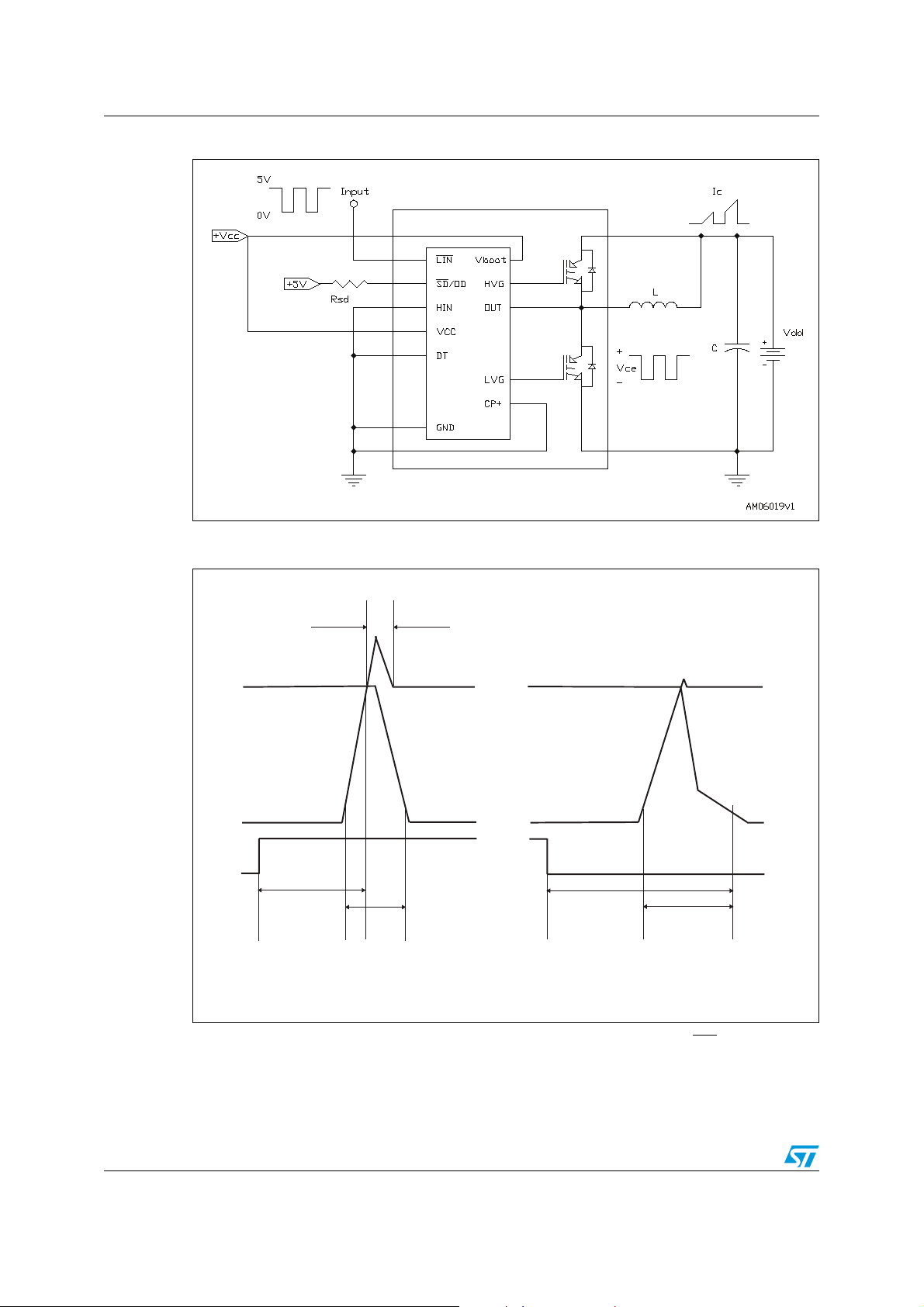
Figure 3. Switching time test circuit
Figure 4. Switching time definition
100% IC 100% IC
t
rr
IC IC
VIN
t
OFF
VIN(OFF)
10% VCE 10% IC
VIN(ON)
VIN
VCE
t
ON
10% IC 90% IC 10% VCE
t
C(ON)
(a) turn-on
Note: Figure 4 "Switching time definition" refers to HIN inputs (active high). For LIN
low), VIN polarity must be inverted for turn-on and turn-off.
t
C(OFF)
(b) turn-off
VCE
AM09223V1
inputs (active
8/20 Doc ID 15927 Rev 6
Page 9
STGIPS14K60 Electrical characteristics
3.1 Control part
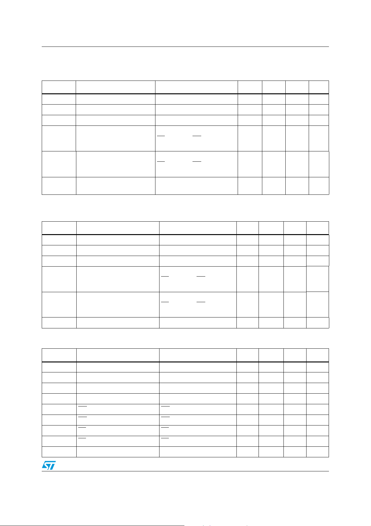
Table 8. Low voltage power supply (VCC = 15 V)
Symbol Parameter Test conditions Min. Typ. Max. Unit
V
cc_hys
V
cc_thONVcc
V
cc_thOFFVcc
I
qccu
I
qcc
Vcc UV hysteresis 1.2 1.5 1.8 V
UV turn ON threshold 11.5 12 12.5 V
UV turn OFF threshold 10 10.5 11 V
Undervoltage quiescent
supply current
Quiescent current
VCC = 10 V
SD/OD = 5 V; LIN = 5 V;
HIN = 0, CIN = 0
= 15 V
V
cc
/OD = 5 V; LIN = 5 V
SD
450 µA
3.5 mA
HIN = 0, CIN = 0
V
ref
Internal comparator (CIN)
reference voltage
0.5 0.54 0.58 V
Table 9. Bootstrapped voltage (VCC = 15 V)
Symbol Parameter Test conditions Min. Typ. Max. Unit
V
BS_hys
V
BS_thON
V
BS_thOFF
I
QBSU
I
QBS
V
UV hysteresis 1.2 1.5 1.8 V
BS
V
UV turn ON threshold 10.6 11.5 12.4 V
BS
V
UV turn OFF threshold 9.1 10 10.9 V
BS
Undervoltage VBS quiescent
current
VBS quiescent current
VBS = 10 V
/OD = 5 V; LIN and
SD
HIN = 5 V; CIN = 0
= 15 V
V
BS
/OD = 5 V; LIN and
SD
70 110 µA
150 210 µA
HIN = 5 V; CIN = 0
R
DS(on)
Bootstrap driver on resistance LVG ON 120 Ω
Table 10. Logic inputs (VCC = 15 V)
Symbol Parameter Test conditions Min. Typ. Max. Unit
V
Low logic level voltage 0.8 V
il
V
I
HINh
I
HINl
I
LINl
I
LINh
I
SDh
I
SDl
Dt Dead time see Figure 7 600 ns
High logic level voltage 2.25 V
ih
HIN logic “1” input bias current HIN = 15 V 110 175 260 µA
HIN logic “0” input bias current HIN = 0 V 1 µA
LIN logic “1” input bias current LIN = 0 V 3 6 20 µA
LIN logic “0” input bias current LIN = 15 V 1 µA
SD logic “0” input bias current SD = 15 V 30 120 300 µA
SD logic “1” input bias current SD = 0 V 3 µA
Doc ID 15927 Rev 6 9/20
Page 10
Electrical characteristics STGIPS14K60
Table 11. Sense comparator characteristics (V
= 15 V)
CC
Symbol Parameter Test conditions Min. Typ. Max. Unit
I
ib
V
t
d_comp
Input bias current V
Open drain low level output
ol
voltage
Comparator delay
SR Slew rate C
t
sd
Shut down to high / low side
driver propagation delay
Comparator triggering to high /
t
isd
low side driver turn-off
propagation delay
= 1 V - 3 µA
CP+
= - 3 mA - 0.5 V
I
od
/OD pulled to 5 V through
SD
100 kΩ resistor
= 180 pF; Rpu = 5 kΩ - 60 V/µsec
L
V
= 0, V
OUT
V
= 0 to 3.3 V
IN
boot
= VCC,
- 90 130 ns
50 125 200
Measured applying a voltage
step from 0 V to 3.3 V to pin
CIN
i
50 200 250
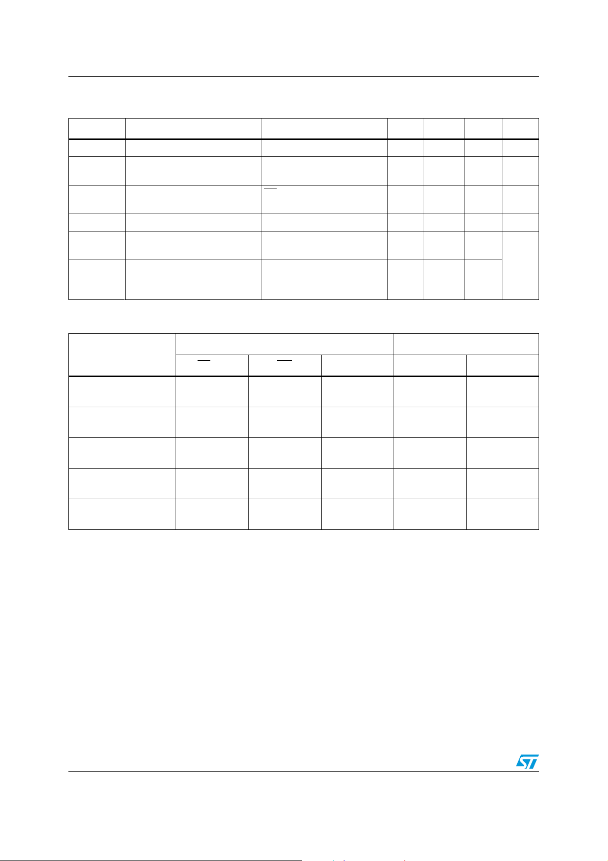
Table 12. Truth table
Condition
Shutdown enable
half-bridge tri-state
Interlocking
half-bridge tri-state
0 ‘’logic state”
half-bridge tri-state
1 “logic state”
low side direct driving
1 “logic state”
high side direct driving
Logic input (V
SD
/OD LIN HIN LVG HVG
LXXLL
HLHLL
HHL L L
HLLHL
HHHLH
)Output
I
ns
Note: X: don’t care
10/20 Doc ID 15927 Rev 6
Page 11
STGIPS14K60 Electrical characteristics
)
C2-3
;!=
F
3).% ;(Z=
FSWK(Z
FSWK(Z
FSWK(Z
6
0.
6-ODULATIONINDEX
0& 4J#4C#
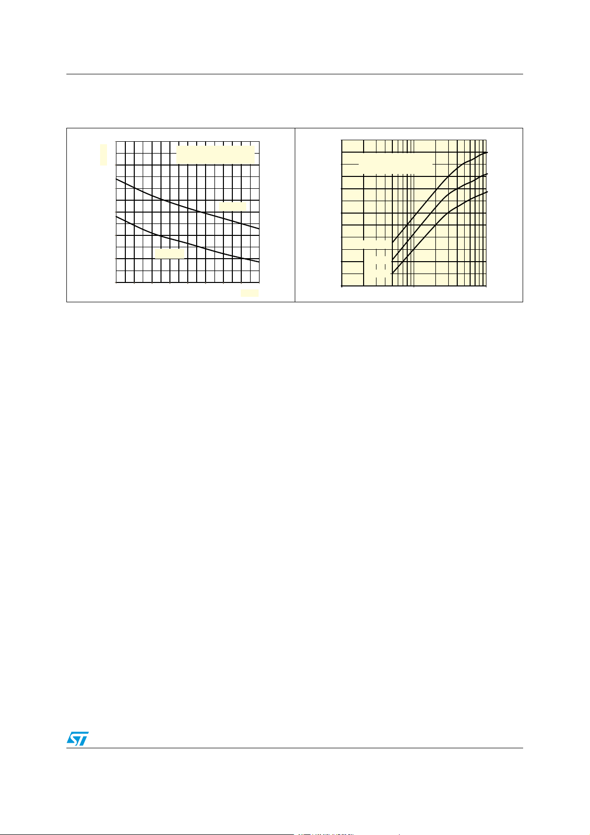
Figure 5. Maximum I
switching frequency
;!=
C2-3
)
4C#
current vs.
C(RMS)
6
6-ODULATIONINDEX
0.
0&4J#F
(1)
3).%
4C#
(Z
F
SW
Figure 6. Maximum I
;K(Z=
1. Simulated curves refer to typical IGBT parameters and maximum R
thj-c.
(1)
C(RMS)
current vs. f
SINE
Doc ID 15927 Rev 6 11/20
Page 12
Electrical characteristics STGIPS14K60
3.2 Waveforms definitions
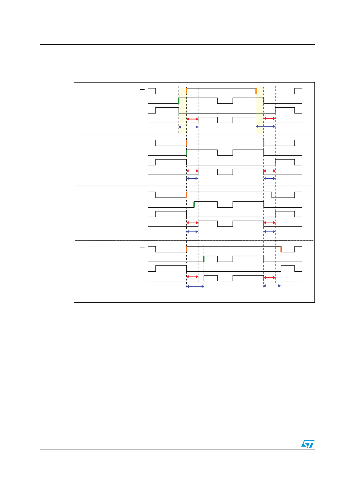
Figure 7. Dead time and interlocking waveforms definitions
LIN
CONTROL SIGNAL EDGES
OVERLAPPED:
INTERLOCKING + DEAD TIME
CONTROL SIGNALS EDGES
SYNCHRONOUS (*):
DEAD TIME
CONTROL SIGNALS EDGES
NOT OVERLAPPED,
BUT INSIDE THE DEAD TIME:
DEAD TIME
HIN
LVG
HVG
gate driver outputs OFF
(HALF-BRIDGE TRI-STATE)
LIN
HIN
LVG
HVG
gate driver outputs OFF
(HALF-BRIDGE TRI-STATE)
LIN
HIN
LVG
HVG
gate driver outputs OFF
(HALF-BRIDGE TRI-STATE)
INTERLOCKING
DTLH
gate driver outputs OFF
(HALF-BRIDGE TRI-STATE)
DTLH DTHL
gate driver outputs OFF
(HALF-BRIDGE TRI-STATE)
LH
DT
gate driver outputs OFF
(HALF-BRIDGE TRI-STATE)
INTERLOCKING
DTHL
DT
HL
CONTROL SIGNALS EDGES
NOT OVERLAPPED,
OUTSIDE THE DEAD TIME:
DIRECT DRIVING
HIN
LVG
HVG
gate driver outputs OFF
(HALF-BRIDGE TRI-STATE)
DTLH
gate driver outputs OFF
(HALF-BRIDGE TRI-STATE)
DTHL
(*) HIN and LIN can be connected together and driven by just one control signal
LIN
12/20 Doc ID 15927 Rev 6
Page 13
STGIPS14K60 Smart shutdown function
4 Smart shutdown function
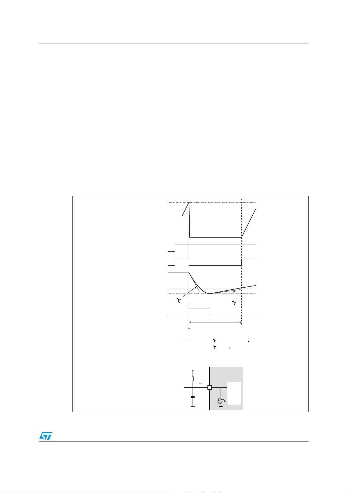
The STGIPS14K60 integrates a comparator for fault sensing purposes. The comparator
non-inverting input (CIN) can be connected to an external shunt resistor in order to
implement a simple over-current protection function. When the comparator triggers, the
device is set in shutdown state and both its outputs are set to low level leading the halfbridge in tri-state. In the common overcurrent protection architectures the comparator output
is usually connected to the shutdown input through a RC network, in order to provide a
mono-stable circuit, which implements a protection time that follows the fault condition. Our
smart shutdown architecture allows to immediately turn-off the output gate driver in case of
overcurrent, the fault signal has a preferential path which directly switches off the outputs.
The time delay between the fault and the outputs turn-off is no more dependent on the RC
values of the external network connected to the shutdown pin. At the same time the internal
logic turns on the open drain output and holds it on until the shutdown voltage goes below
the logic input lower threshold. Finally the smart shutdown function provides the possibility
to increase the real disable time without increasing the constant time of the external RC
network.
Figure 8. Smart shutdown timing waveforms
comp
Vref
CP+
PROTECTION
HIN/LIN
HVG/LVG
SD/OD
upper
threshold
lower
threshold
open drain gate
(internal)
the driver outputs are set in SD state
immediately after the comparator
triggering even if the SD signal
Fast shut down:
has not yet reach
the lower input threshold
1
real disable time
TIME CONSTANTS
= (RON_OD // RSD)
1
= RSD
2
2
C
SD
C
SD
SHUT DOWN CIRCUIT
V
BIAS
RSD
CSD
SD/OD
RON_OD
SMART
SD
LOGIC
FROM/TO
CONTROLLER
Note: Pls refer to Table 11: Sense comparator characteristics (VCC = 15 V) for inter nal
propagation delay time details.
Doc ID 15927 Rev 6 13/20
Page 14
Applications information STGIPS14K60
+
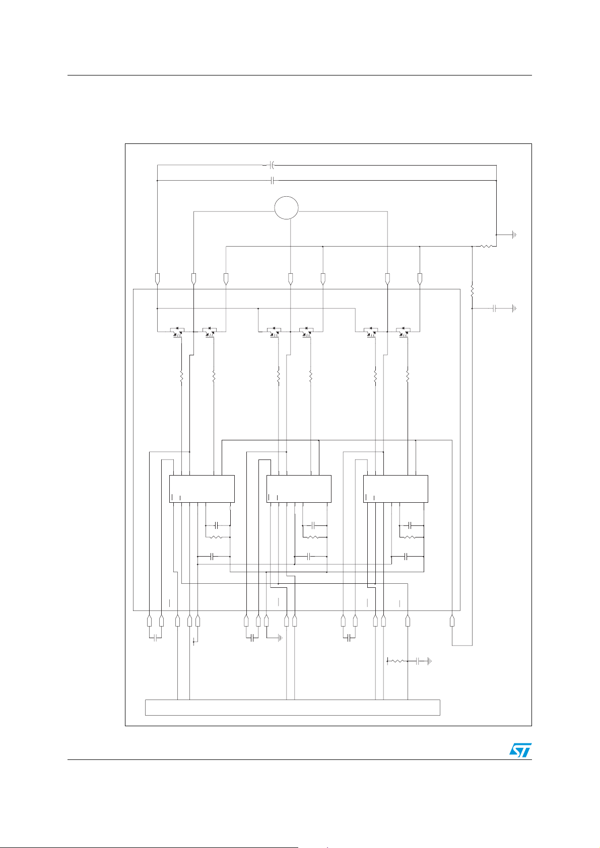
5 Applications information
Figure 9. Typical application circuit
VDC
M
Rshunt
P
U
D1
T1
Rg
OUT
HVG
Vboot
LIN
SD/OD
HIN
Nu
D2
T2
Rg
LVG
CP+
VCC
GND
DT
Cdt
Rdt
Cvcc
V
D3
T3
Rg
OUT
HVG
Vboot
LIN
SD/OD
HIN
Nv
D4
T4
Rg
LVG
CP+
VCC
GND
DT
Rdt Cdt
Cvcc
W
D5
T5
Rg
OUT
HVG
Vboot
LIN
SD/OD
HIN
Nw
D6
R
C
T6
Rg
LVG
CP+
VCC
GND
DT
Cdt
Rdt
Cvcc
VBOOT U
OUT U
Cbu
VCC
HIN-U
LIN-U
OUT V
LIN-V
GND
VBOOT V
Cbv
VCC
CONTROLLER
14/20 Doc ID 15927 Rev 6
HIN-V
HIN-W
LIN-W
VBOOT W
OUT W
Cbw
SD/OD
Rsd
Csd
CIN
3.3V/5V Line
AM05001v1
Page 15
STGIPS14K60 Applications information
5.1 Recommendations
● Input signal HIN is active high logic. A 85 kΩ (typ.) pull down resistor is built-in for each high side
input. If an external RC filter is used, for noise immunity, pay attention to the variation of the input
signal level.
● Input signal /LIN is active low logic. A 720 kΩ (typ.) pull-up resistor, connected to an
internal 5V regulator through a diode, is built-in for each low side input.
● To prevent the input signals oscillation, the wiring of each input should be as short as
possible.
● By integrating an application specific type HVIC inside the module, direct coupling to
MCU terminals without any opto-coupler is possible.
● Each capacitor should be located as nearby the pins of IPM as possible.
● Low inductance shunt resistors should be used for phase leg current sensing.
● Electrolytic bus capacitors should be mounted as close to the module bus terminals as
possible. Additional high frequency ceramic capacitor mounted close to the module
pins will further improve performance.
● The SD/OD signal should be pulled up to 5 V / 3.3 V with an external resistor (see
Section 4: Smart shutdown function for detailed info).
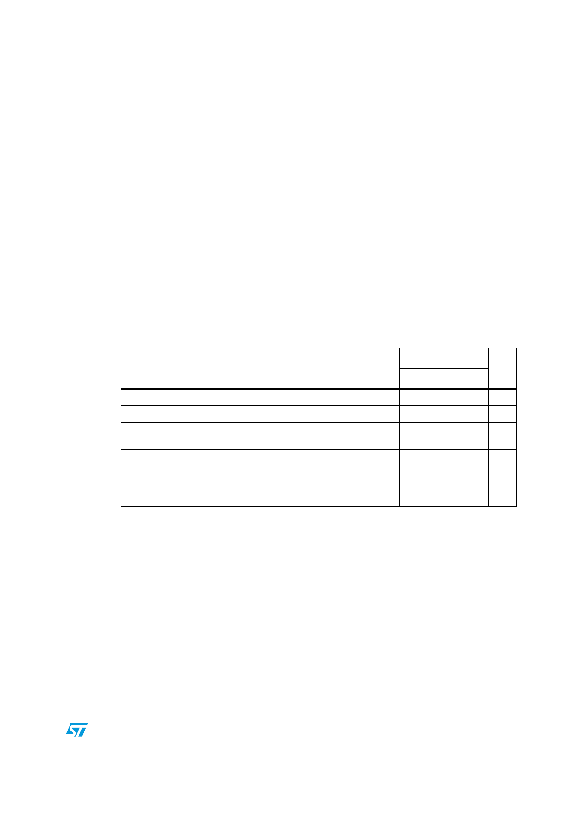
Table 13. Recommended operating conditions
Symbol Parameter Conditions
V
V
V
t
dead
f
PWM
PN
CC
BS
Supply Voltage Applied between P-Nu, Nv, Nw 300 400 V
Control supply voltage Applied between VCC-GND 13.5 15 18 V
High side bias voltage
Blanking time to
prevent Arm-short
PWM input signal
Applied between V
i = U, V, W
For each input signal 1 µs
-40°C < T
< 100°C
c
-40°C < Tj < 125°C
BOOTi
-OUTi for
Val ue
Unit
Min. Typ. Max.
13 18 V
20 kHz
Doc ID 15927 Rev 6 15/20
Page 16
Package mechanical data STGIPS14K60
6 Package mechanical data
In order to meet environmental requirements, ST offers these devices in different grades of
ECOPACK
specifications, grade definitions and product status are available at: www.st.com.
ECOPACK
®
packages, depending on their level of environmental compliance. ECOPACK®
®
is an ST trademark.
Please refer to dedicated technical note TN0107 for mounting instructions.
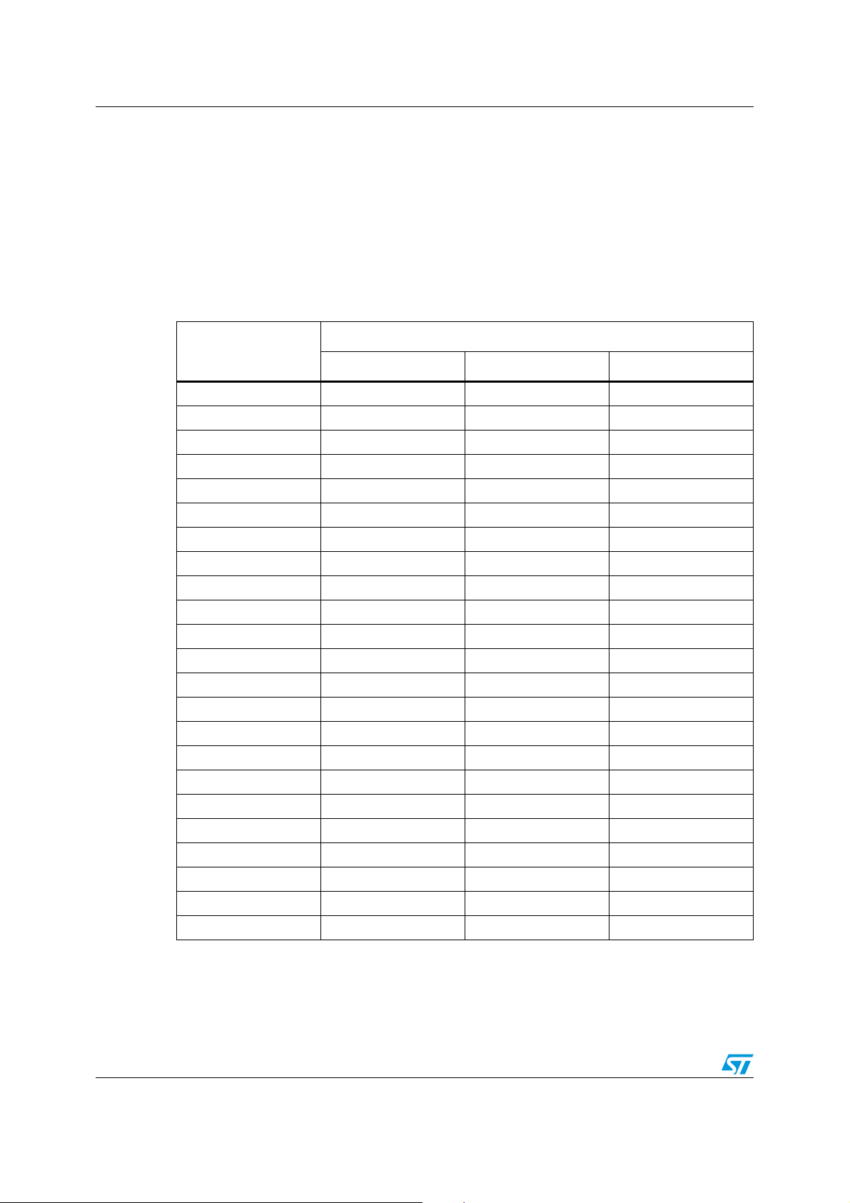
Table 14. SDIP-25L mechanical data
(mm.)
Dim.
Min. Typ. Max.
A 43.90 44.40 44.90
A1 1.15 1.35 1.55
A2 1.40 1.60 1.80
A3 38.90 39.40 39.90
B 21.50 22.00 22.50
B1 11.25 11.85 12.45
B2 24.70 25.20 25.70
C 5.00 5.40 6.00
C1 6.50 7.00 7.50
C2 11.20 11.70 12.20
e 2.15 2.35 2.55
e1 3.40 3.60 3.80
e2 4.50 4.70 4.90
e3 6.30 6.50 6.70
D33.30
D1 5.55
E11.20
E1 1.40
F 0.85 1.00 1.15
F1 0.35 0.50 0.65
R 1.55 1.75 1.95
T 0.45 0.55 0.65
V0° 6°
16/20 Doc ID 15927 Rev 6
Page 17
STGIPS14K60 Package mechanical data
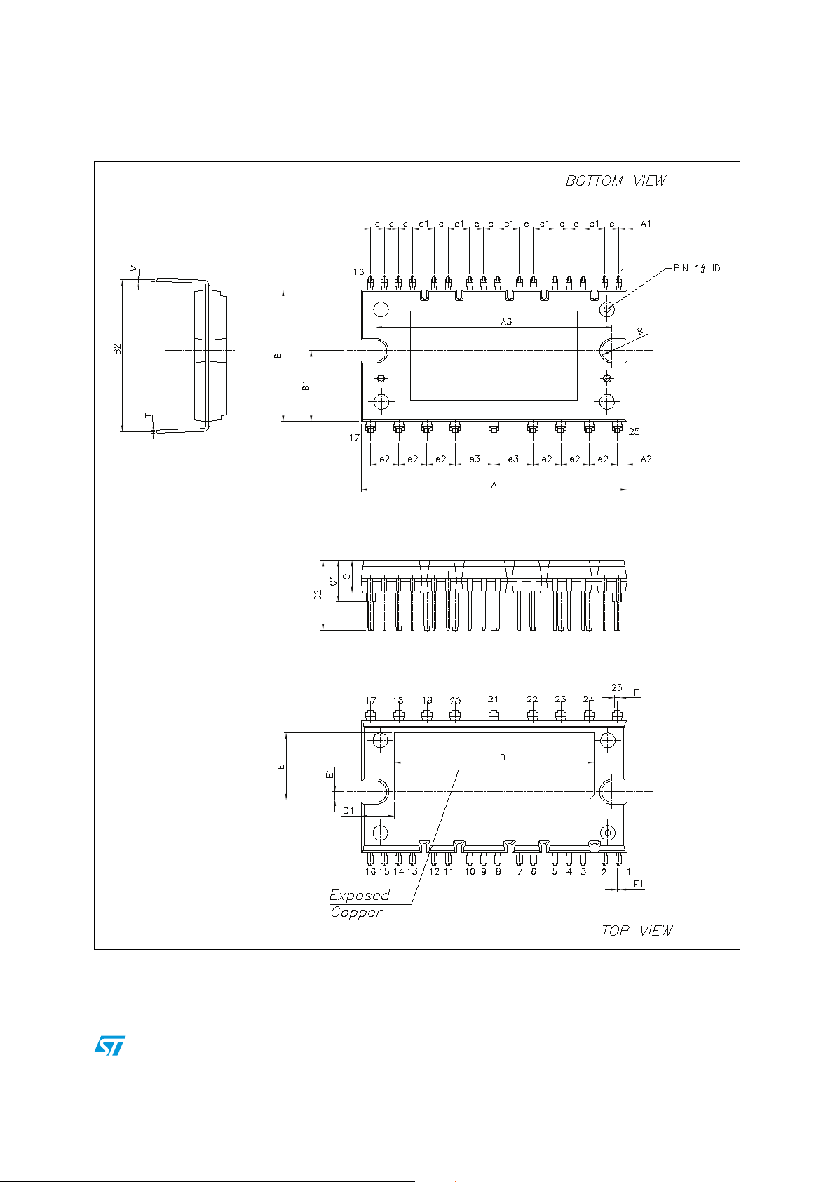
Figure 10. SDIP-25L drawing dimensions data
8154676_G
Doc ID 15927 Rev 6 17/20
Page 18
Package mechanical data STGIPS14K60
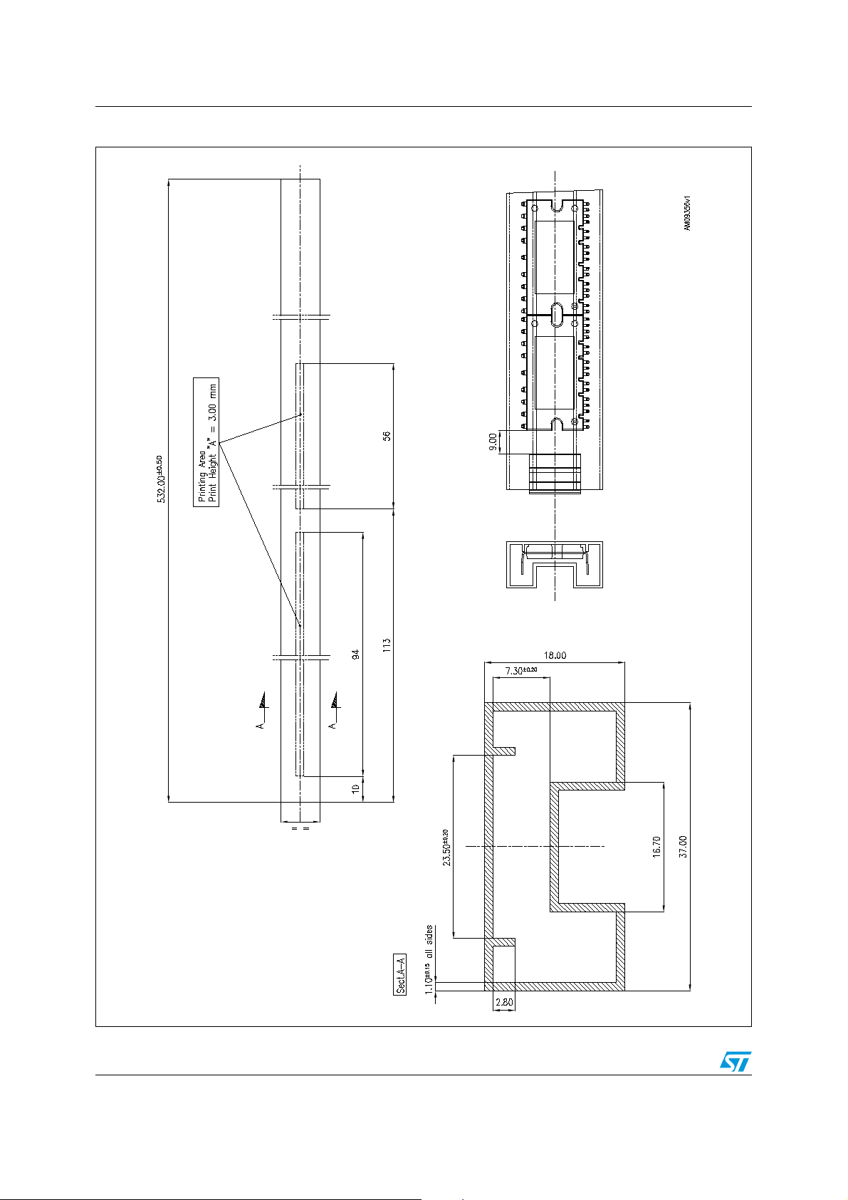
Figure 11. SDIP-25L tube dimensions
18/20 Doc ID 15927 Rev 6
8304142_A
Page 19
STGIPS14K60 Revision history
7 Revision history
Table 15. Document revision history
Date Revision Changes
25-Jun-2009 1 Initial release.
05-Aug-2009 2 Reduced V
Document status promoted from preliminary data to datasheet.
Updated package mechanical data, Table 7: Inverter part,
15-Jun-2010 3
Figure 5: Maximum IC(RMS) current vs. switching frequency
and Figure 6: Maximum IC(RMS) current vs. fSINE (1).
Minor text changes to improve readability.
value on Ta bl e 7 .
CE(sat)
08-Nov-2010 4
09-Mar-2011 5
04-Nov-2011 6
Updated Ta b le 3 , 5, 8, 9, 10 and Ta bl e 1 1 .
Modified: Figure 5 and Figure 6.
Updated title with SLLIMM™ in cover page, added SDIP-25L
tube dimensions Figure 11 on page 18.
Updated title with SLLIMM™ (small low-loss intelligent molded
module) IPM, 3-phase inverter - 14 A, 600 V short-circuit
rugged IGBT in cover page and SDIP-25L mechanical data
Table 14 on page 16, Figure 10 on page 17.
Doc ID 15927 Rev 6 19/20
Page 20

STGIPS14K60
Please Read Carefully:
Information in this document is provided solely in connection with ST products. STMicroelectronics NV and its subsidiaries (“ST”) reserve the
right to make changes, corrections, modifications or improvements, to this document, and the products and services described herein at any
time, without notice.
All ST products are sold pursuant to ST’s terms and conditions of sale.
Purchasers are solely responsible for the choice, selection and use of the ST products and services described herein, and ST assumes no
liability whatsoever relating to the choice, selection or use of the ST products and services described herein.
No license, express or implied, by estoppel or otherwise, to any intellectual property rights is granted under this document. If any part of this
document refers to any third party products or services it shall not be deemed a license grant by ST for the use of such third party products
or services, or any intellectual property contained therein or considered as a warranty covering the use in any manner whatsoever of such
third party products or services or any intellectual property contained therein.
UNLESS OTHERWISE SET FORTH IN ST’S TERMS AND CONDITIONS OF SALE ST DISCLAIMS ANY EXPRESS OR IMPLIED
WARRANTY WITH RESPECT TO THE USE AND/OR SALE OF ST PRODUCTS INCLUDING WITHOUT LIMITATION IMPLIED
WARRANTIES OF MERCHANTABILITY, FITNESS FOR A PARTICULAR PURPOSE (AND THEIR EQUIVALENTS UNDER THE LAWS
OF ANY JURISDICTION), OR INFRINGEMENT OF ANY PATENT, COPYRIGHT OR OTHER INTELLECTUAL PROPERTY RIGHT.
UNLESS EXPRESSLY APPROVED IN WRITING BY TWO AUTHORIZED ST REPRESENTATIVES, ST PRODUCTS ARE NOT
RECOMMENDED, AUTHORIZED OR WARRANTED FOR USE IN MILITARY, AIR CRAFT, SPACE, LIFE SAVING, OR LIFE SUSTAINING
APPLICATIONS, NOR IN PRODUCTS OR SYSTEMS WHERE FAILURE OR MALFUNCTION MAY RESULT IN PERSONAL INJURY,
DEATH, OR SEVERE PROPERTY OR ENVIRONMENTAL DAMAGE. ST PRODUCTS WHICH ARE NOT SPECIFIED AS "AUTOMOTIVE
GRADE" MAY ONLY BE USED IN AUTOMOTIVE APPLICATIONS AT USER’S OWN RISK.
Resale of ST products with provisions different from the statements and/or technical features set forth in this document shall immediately void
any warranty granted by ST for the ST product or service described herein and shall not create or extend in any manner whatsoever, any
liability of ST.
ST and the ST logo are trademarks or registered trademarks of ST in various countries.
Information in this document supersedes and replaces all information previously supplied.
The ST logo is a registered trademark of STMicroelectronics. All other names are the property of their respective owners.
© 2011 STMicroelectronics - All rights reserved
Australia - Belgium - Brazil - Canada - China - Czech Republic - Finland - France - Germany - Hong Kong - India - Israel - Italy - Japan -
STMicroelectronics group of companies
Malaysia - Malta - Morocco - Philippines - Singapore - Spain - Sweden - Switzerland - United Kingdom - United States of America
www.st.com
20/20 Doc ID 15927 Rev 6
 Loading...