

Page 1
STD1NB50
N - CHANNEL 500V - 7.5Ω - 1.4A IPAK
PowerMESH MOSFET
TYPE V
DSS
R
DS(on)
I
D
ST D1N B5 0 500V < 9 Ω 1.4 A
■ TYPICALR
■ EXTREMELYHIGH dv/dt CAPABILITY
■ 100%AVALANCHETESTED
■ VERYLOW INTRINSIC CAPACITANCES
■ GATECHARGE MINIMIZED
■ FORSMD DPAK VERSIONCONTACT
DS(on)
= 7.5 Ω
SALESOFFICE
DESCRIPTION
Using the latest high voltage MESH OVERLAY
process, STMicroelectronics has designed an
advanced family of power MOSFETs with
outstanding performances. The new patent
pending strip layout coupled with the Company’s
proprietary edge termination structure, gives the
lowest R
per area, exceptional avalanche
DS(on)
and dv/dt capabilities and unrivalled gate charge
and switching characteristics.
APPLICATIONS
■ SWITCHMODE POWER SUPPLIES (SMPS)
■ DC-AC CONVERTERS FOR WELDING
EQUIPMENTANDUNINTERRUPTIBLE
POWERSUPPLIESAND MOTOR DRIVE
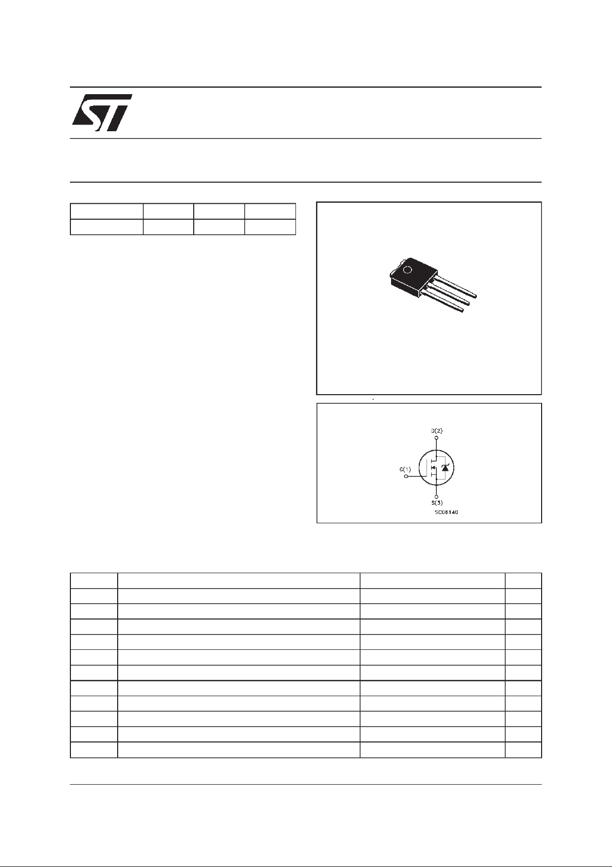
3
2
1
IPAK
TO-251
(Suffix”-1”)
INTERNAL SCHEMATIC DIAGRAM
ABSOLUTE MAXIMUM RATINGS
Symbol Parameter Value Unit
V
V
V
I
DM
P
dv/dt(
T
(•) Pulsewidth limitedby safe operating area (1)ISD≤1.4A, di/dt ≤ 150 A/µs, VDD≤ V
March 2000
Dra in- sour c e Volt age (VGS= 0) 500 V
DS
Dra in- gat e V ol t age (RGS=20kΩ) 500 V
DGR
Gat e-source Volt age ± 36 V
GS
I
Dra in Cu rr ent (continuous ) a t Tc=25oC1.4A
D
I
Dra in Cu rr ent (continuous ) a t Tc=100oC0.91A
D
(•) Drain Curr ent (pulsed ) 5.6 A
Tot al Diss ipation at Tc=25oC45W
tot
Der ati ng Fact or 0.36 W/
1) Peak Di ode Recovery voltage slope 3.5 V/ns
St orage T emperatur e -65 to 150
stg
T
Max. Operating J unction Tem perature 150
j
,Tj≤T
(BR)DSS
JMAX
o
C
o
C
o
C
1/8
Page 2
STD1NB50
THERMAL DATA
R
thj-case
Rthj-amb
R
thc-sink
T
AVALANCHE CHARACTERISTICS
Symbol Parameter Max Value Unit
I
AR
E
Ther mal Resistanc e Junct ion-case Max
Ther mal Resistanc e Junct ion-ambient Max
Ther mal Resistanc e Case-sink Ty p
Maximum L ead Temperature F or Solder ing P urpose
l
Avalanche Current, Repetitive or Not-Repetitive
(pulse width limited by T
Single Pul se A v alan c he E nergy
AS
(starting T
=25oC, ID=IAR,VDD=50V)
j
max,δ <1%)
j
2.78
100
1.5
275
1.4 A
40 mJ
o
C/W
oC/W
o
C/W
o
C
ELECTRICAL CHARACTERISTICS
=25oC unless otherwisespecified)
(T
case
OFF
Symbol Parameter Test Conditions Min. Typ. Max. Unit
V
(BR)DSS
Drain-source
ID=250µAVGS= 0 500 V
Break dow n Vo lt age
I
DSS
I
GSS
Zero Gate Voltage
Drain Curre nt (V
GS
Gat e- bod y Leakag e
Current (V
DS
=0)
=0)
V
=MaxRating
DS
=MaxRating Tc=125oC
V
DS
V
=± 30 V
GS
1
50
100 nA
±
ON(∗)
Symbol Parameter Test Conditions Min. Typ. Max. Unit
V
GS(th)
R
DS(on)
Gate Threshold Voltage VDS=VGSID= 250 µA 234V
Sta t ic Drain-s our c e On
VGS=10V ID=0.5 A 7.5 9
Resistance
I
D(on)
On State Drain Current VDS>I
D(on)xRDS(on)max
1.4 A
VGS=10V
DYNAMIC
Symbol Parameter Test Conditions Min. Typ. Max. Unit
g
(∗)Forward
fs
Tr ansc on duc tance
C
C
C
Input Capacit ance
iss
Out put Capac itance
oss
Reverse Transfer
rss
Capacit a nc e
VDS>I
D(on)xRDS(on)maxID
= 0.7 A 0.45 0.7 S
VDS=25V f=1MHz VGS= 0 150
24
2.5
200
32
3.3
µ
µA
Ω
pF
pF
pF
A
2/8
Page 3
STD1NB50
ELECTRICAL CHARACTERISTICS
(continued)
SWITCHING ON
Symbol Parameter Test Conditions Min. Typ. Max. Unit
t
d(on)
t
r
Turn-on Time
Rise T ime
VDD=250V ID=0.7A
R
=4.7
G
Ω
VGS=10V
8
8
12
12
(see test circuit, figure 3)
Q
Q
Q
Tot al Gate Charge
g
Gat e- Source Charge
gs
Gate-Drain Charge
gd
VDD= 400 V ID=1.4 A VGS=10V 9
5.5
2.4
13 nC
SWITCHING OFF
Symbol Parameter Test Conditions Min. Typ. Max. Unit
t
r(Voff)
t
t
Off-voltage Rise Time
Fall T ime
f
Cross-over Tim e
c
VDD=400V ID= 1.4 A
=4.7 Ω VGS=10V
R
G
(see test circuit, figure 5)
20
22
30
28
31
42
SOURCEDRAINDIODE
Symbol Parameter Test Conditions Min. Typ. Max. Unit
I
SD
I
SDM
V
SD
t
Q
I
RRM
(∗) Pulsed:Pulse duration = 300µs, duty cycle 1.5%
(•) Pulse width limited by safeoperating area
Source-drain Current
(•)
Source-drain Current
1.4
5.6
(pulsed)
(∗)ForwardOnVoltage ISD=1.4A VGS=0 1.6 V
Reverse Recovery
rr
Time
Reverse Recovery
rr
ISD= 1.4 A di/dt = 100 A/µs
= 100 V Tj=150oC
V
DD
(see test circuit, figure 5)
330
780
Charge
Reverse Recovery
4.7
Current
ns
ns
nC
nC
ns
ns
ns
A
A
ns
nC
A
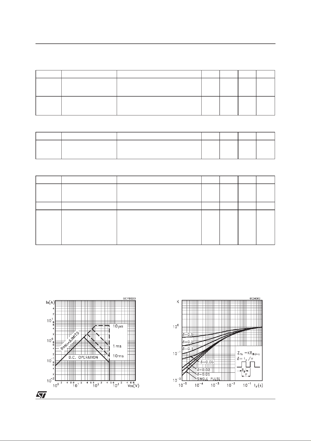
SafeOperating Area ThermalImpedance
3/8
Page 4

STD1NB50
OutputCharacteristics
Transconductance
TransferCharacteristics
Static Drain-sourceOn Resistance
Gate Charge vs Gate-sourceVoltage
4/8
CapacitanceVariations
Page 5

STD1NB50
NormalizedGate ThresholdVoltage vs
Temperature
Source-drainDiode Forward Characteristics
NormalizedOn Resistancevs Temperature
5/8
Page 6

STD1NB50
Fig. 1:
UnclampedInductiveLoad TestCircuit
Fig. 3: SwitchingTimes Test Circuits For
ResistiveLoad
Fig. 2:
UnclampedInductive Waveform
Fig. 4: Gate Charge test Circuit
Fig. 5:
Test Circuit For InductiveLoad Switching
And Diode Recovery Times
6/8
Page 7

TO-251 (IPAK) MECHANICALDATA
STD1NB50
DIM.
mm inch
MIN. TYP. MAX. MIN. TYP. MAX.
A 2.2 2.4 0.086 0.094
A1 0.9 1.1 0.035 0.043
A3 0.7 1.3 0.027 0.051
B 0.64 0.9 0.025 0.031
B2 5.2 5.4 0.204 0.212
B3 0.85 0.033
B5 0.3 0.012
B6 0.95 0.037
C 0.45 0.6 0.017 0.023
C2 0.48 0.6 0.019 0.023
D 6 6.2 0.236 0.244
E 6.4 6.6 0.252 0.260
G 4.4 4.6 0.173 0.181
H 15.9 16.3 0.626 0.641
L 9 9.4 0.354 0.370
L1 0.8 1.2 0.031 0.047
L2 0.8 1 0.031 0.039
A
E
==
C2
L2
B2
==
H
C
A3
A1
B6
L
B
B5
G
==
D
B3
2
13
L1
0068771-E
7/8
Page 8

STD1NB50
Information furnished is believed tobeaccurate and reliable.However, STMicroelectronics assumes no responsibility for the consequences
of use of such information nor for any infringement of patents or other rights of third parties which may result from its use. No licenseis
granted by implication orotherwise under anypatent or patent rights of STMicroelectronics. Specificationmentioned in this publicationare
subjectto change without notice. Thispublication supersedes and replacesall information previouslysupplied.STMicroelectronicsproducts
are not authorized for use as critical components in lifesupport devices or systems without express written approval of STMicroelectronics.
The STlogo is a trademark of STMicroelectronics
1999STMicroelectronics – Printed in Italy – All RightsReserved
STMicroelectronics GROUP OF COMPANIES
Australia - Brazil - China- Finland - France - Germany - Hong Kong - India - Italy- Japan - Malaysia - Malta - Morocco-
8/8
Singapore - Spain - Sweden - Switzerland - United Kingdom- U.S.A.
http://www.st.com
.
 Loading...