

Page 1
STD19NE06L
N - CHANNEL 60V - 0.038 Ω - 19A - TO-251/TO-252
STripFET POWER MOSFET
TYPE V
DSS
R
DS(o n)
I
D
ST D19N E 06L 60 V < 0 . 05 Ω 19 A
■ TYPICALR
■ 100%AVALANCHETESTED
■ LOW GATE CHARGE
■ APPLICATIONORIENTED
DS(on)
= 0.038 Ω
CHARACTERIZATION
■ ADDSUFFIX ”T4” FORORDERING INTAPE
& REEL
DESCRIPTION
This PowerMOSFET is the latest developmentof
STMicroelectronics unique ”Single Feature
Size” strip-based process. The resulting transi-
stor showsextremelyhigh packing densityfor low
on-resistance, rugged avalanche characteristics
and less critical alignment steps therefore a remarkablemanufacturingreproducibility.
APPLICATIONS
■ HIGHCURRENT, HIGH SPEEDSWITCHING
■ SOLENOIDAND RELAYDRIVERS
■ MOTORCONTROL, AUDIOAMPLIFIERS
■ DC-DC& DC-ACCONVERTERS
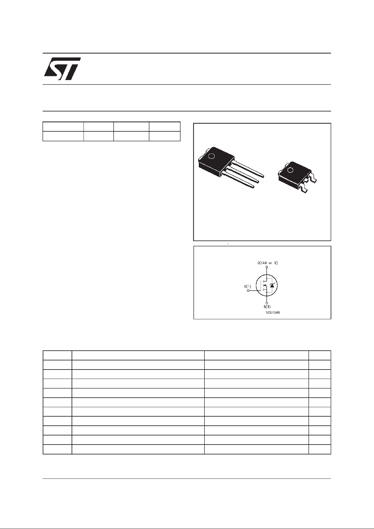
3
2
IPAK
TO-251
(Suffix”-1”)
1
(Suffix ”T4”)
1
DPAK
TO-252
INTERNAL SCHEMATIC DIAGRAM
3
ABSOLUTE MAXIMUM RATINGS
Symbol Parameter Value Uni t
V
V
V
I
DM
P
T
(•) Pulse width limited by safe operating area
February 1999
Drain-source Voltage (VGS=0) 60 V
DS
Drain- gate Voltage (RGS=20kΩ)60V
DGR
Gate-source Voltage
GS
I
Drain Current (cont in uous) at Tc=25oC19A
D
I
Drain Current (cont in uous) at Tc=100oC13A
D
20 V
±
(•) Drain Current (pulsed) 76 A
Total Dissipation at Tc=25oC45W
tot
Derat ing Factor 0.3 W/
Sto rage Tem perature -65 to 175
stg
T
Max. Operati ng Junct ion Tempe r ature 175
j
o
C
o
C
o
C
1/9
Page 2
STD19NE06L
THERMAL DATA
R
thj-case
R
thj-amb
R
thc-sink
T
AVALANCHE CHARACTERISTICS
Symbol Parameter Max Value Unit
I
AR
E
Ther mal Resistanc e Junct ion-case Max
Ther mal Resistanc e Junct ion-ambient Max
Ther mal Resistanc e Case-sink Ty p
Maximum Lead Te m perature F or Soldering Purpose
l
Avalanche C urrent, R epetitive or Not-Repetitive
(pulse width limited by T
Single Pulse A v alan c he Energy
AS
(starting T
=25oC, ID=IAR,VDD=35V)
j
max)
j
3.33
100
1.5
275
19 A
50 mJ
o
C/W
o
C/W
o
C/W
o
C
ELECTRICAL CHARACTERISTICS
=25oC unless otherwisespecified)
(T
case
OFF
Symbol Parameter Test Conditions Min. Typ. Max. Unit
V
(BR)DSS
Drain-source
ID=250µAVGS=0 60 V
Break dow n Volt age
I
DSS
I
GSS
Zero Gate Voltage
Drain Current (V
GS
Gat e- bod y Leakage
Current (V
DS
=0)
=0)
V
=MaxRating
DS
=MaxRating Tc= 125oC
V
DS
V
=± 20 V
GS
1
10
100 nA
±
ON(∗)
Symbol Parameter Test Conditions Min. Typ. Max. Unit
V
GS(th)
R
DS(on)
I
D(on)
Gate Threshold Voltage VDS=VGSID= 250 µ A11.72.5V
Sta t ic Drain-sour c e On
Resistance
VGS=5V ID=9.5A
= 10V ID=9.5A
V
GS
On State Drain Current VDS>I
D(on)xRDS(on )max
0.048
0.038
19 A
0.06
0.05
VGS=10V
DYNAMIC
Symbol Parameter Test Conditions Min. Typ. Max. Unit
g
(∗)Forward
fs
Tr ansc on duc tance
C
C
C
Input Capacitanc e
iss
Out put Capacitance
oss
Reverse Transfer
rss
Capacit a nc e
VDS>I
D(on)xRDS(on )maxID
=9.5A 7 14 S
VDS=25V f=1MHz VGS= 0 1350
195
58
µ
µA
Ω
Ω
pF
pF
pF
A
2/9
Page 3
STD19NE06L
ELECTRICAL CHARACTERISTICS
(continued)
SWITCHING ON
Symbol Parameter Test Conditions Min. Typ. Max. Unit
t
d(on)
Tur n-on Delay Time
Rise Time
t
r
VDD=30V ID=15A
R
=4.7
G
Ω
VGS=4.5V
25
105
(Resis t iv e Load, see fig. 3)
Q
Q
Q
Tot al Gate Charge
g
Gat e- Source Char g e
gs
Gate-Drain Charge
gd
VDD=48V ID=30A VGS=5V 20
8
10
28 nC
SWITCHING OFF
Symbol Parameter Test Conditions Min. Typ. Max. Unit
t
d(off)
Tur n-of f Delay Time
t
Fall T ime
f
VDD=30V ID=15A
=4.7 Ω VGS=4.5V
R
G
50
20
(Resis t iv e Load, see fig. 3)
t
r(Voff)
t
t
Off-volt age Rise T ime
Fall T ime
f
Cross-over Time
c
VDD=48V ID=30A
=4.7 Ω VGS=4.5V
R
G
(Indu ct iv e Load, see fig. 5)
15
40
60
SOURCEDRAIN DIODE
Symbol Parameter Test Conditions Min. Typ. Max. Unit
I
V
I
SDM
SD
Q
I
RRM
SD
t
Source-drain Current
(•)
Source-drain Current
19
76
(pulsed)
(∗)ForwardOnVoltage ISD=30A VGS=0 1.5 V
Reverse Recovery
rr
Time
Reverse Recovery
rr
ISD= 30 A di/dt = 100 A/µs
=30V Tj=150oC
V
DD
(see test circuit, fig. 5)
80
0.18
Charge
Reverse Recovery
4.5
Current
ns
ns
nC
nC
ns
ns
ns
ns
ns
A
A
ns
µC
A
(∗) Pulsed:Pulse duration = 300µs, dutycycle 1.5%
(•) Pulse width limited by safeoperating area
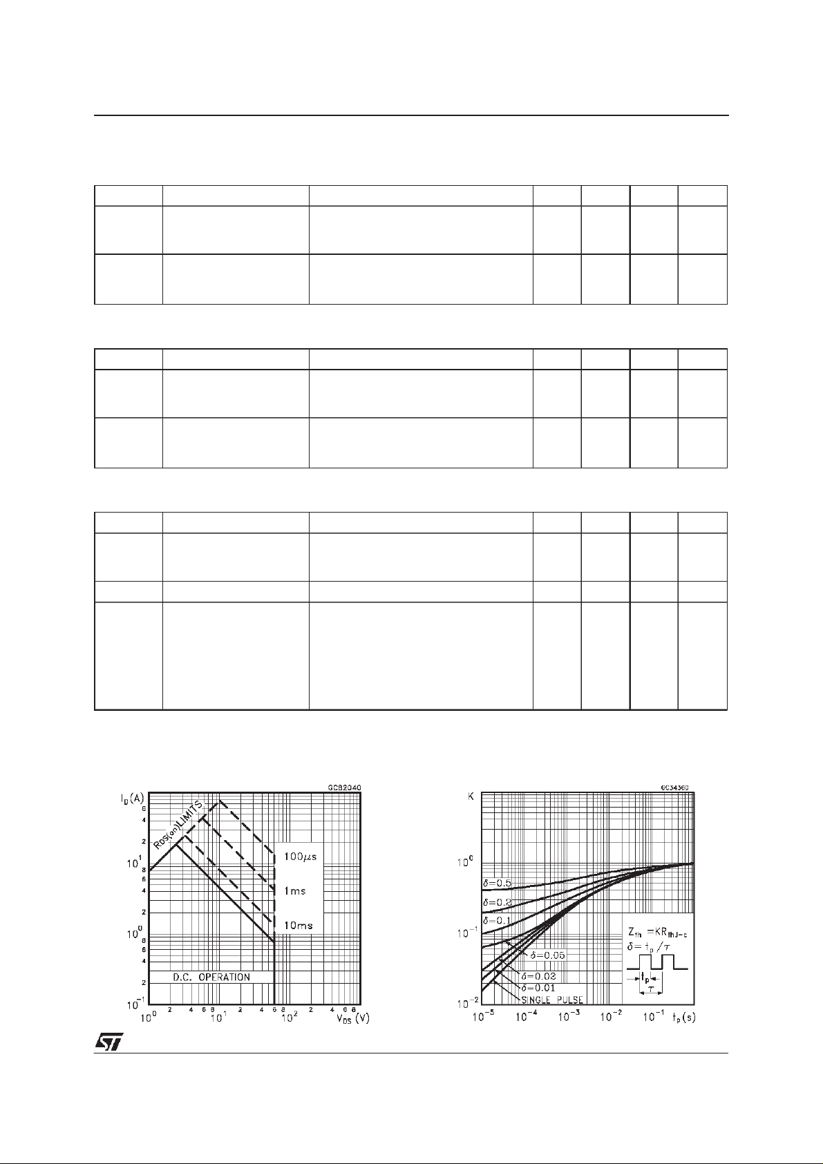
SafeOperating Area ThermalImpedance
3/9
Page 4

STD19NE06L
OutputCharacteristics
Transconductance
TransferCharacteristics
Static Drain-sourceOn Resistance
Gate Charge vs Gate-sourceVoltage
4/9
CapacitanceVariations
Page 5

STD19NE06L
NormalizedGate ThresholdVoltage vs
Temperature
Source-drainDiode Forward Characteristics
NormalizedOn Resistancevs Temperature
5/9
Page 6

STD19NE06L
Fig. 1:
UnclampedInductiveLoad TestCircuit
Fig. 3: SwitchingTimes Test Circuits For
ResistiveLoad
Fig. 2:
UnclampedInductiveWaveform
Fig. 4: Gate Charge test Circuit
Fig. 5:
Test Circuit For InductiveLoad Switching
And Diode Recovery Times
6/9
Page 7

TO-251 (IPAK) MECHANICALDATA
STD19NE06L
DIM.
mm inch
MIN. TYP. MAX. MIN. TYP. MAX.
A 2.2 2.4 0.086 0.094
A1 0.9 1.1 0.035 0.043
A3 0.7 1.3 0.027 0.051
B 0.64 0.9 0.025 0.031
B2 5.2 5.4 0.204 0.212
B3 0.85 0.033
B5 0.3 0.012
B6 0.95 0.037
C 0.45 0.6 0.017 0.023
C2 0.48 0.6 0.019 0.023
D 6 6.2 0.236 0.244
E 6.4 6.6 0.252 0.260
G 4.4 4.6 0.173 0.181
H 15.9 16.3 0.626 0.641
L 9 9.4 0.354 0.370
L1 0.8 1.2 0.031 0.047
L2 0.8 1 0.031 0.039
A
E
==
C2
L2
B2
==
H
C
A3
A1
B6
L
B
B5
G
==
D
B3
2
13
L1
0068771-E
7/9
Page 8

STD19NE06L
TO-252 (DPAK) MECHANICALDATA
DIM.
mm inch
MIN. TYP. MAX. MIN. TYP. MAX.
A 2.2 2.4 0.086 0.094
A1 0.9 1.1 0.035 0.043
A2 0.03 0.23 0.001 0.009
B 0.64 0.9 0.025 0.035
B2 5.2 5.4 0.204 0.212
C 0.45 0.6 0.017 0.023
C2 0.48 0.6 0.019 0.023
D 6 6.2 0.236 0.244
E 6.4 6.6 0.252 0.260
G 4.4 4.6 0.173 0.181
H 9.35 10.1 0.368 0.397
L2 0.8 0.031
L4 0.6 1 0.023 0.039
8/9
H
A
E
==
C2
L2
B2
==
DETAIL”A”
D
2
13
L4
A1
C
A2
DETAIL”A”
B
G
==
0068772-B
Page 9

STD19NE06L
Information furnished is believed tobeaccurateand reliable. However, STMicroelectronics assumes no responsibilityforthe consequences
of use of such information nor for any infringement of patents or other rights of third parties which may result from its use. No license is
granted by implication or otherwise under any patent or patent rights of STMicroelectronics. Specificationmentioned in this publicationare
subjecttochange without notice.Thispublication supersedesand replacesall information previouslysupplied.STMicroelectronics products
are not authorizedfor useas critical components in lifesupport devices or systems without express written approval of STMicroelectronics.
The STlogo is a trademark of STMicroelectronics
1999 STMicroelectronics – Printed in Italy – All Rights Reserved
STMicroelectronics GROUP OF COMPANIES
Australia - Brazil - Canada - China -France - Germany - Italy- Japan- Korea- Malaysia - Malta - Mexico - Morocco - The Netherlands -
Singapore - Spain - Sweden - Switzerland - Taiwan- Thailand - UnitedKingdom - U.S.A.
http://www.st.com
.
9/9
 Loading...