

Page 1
N - CHANNEL 100V - 0.014Ω - 80A I2PAK/D2PAK
LOW Qg STripFET POWER MOSFET
TYPE V
DSS
ST B80NF10 100 V < 0.0 18 Ω 80 A
■ TYPICALR
■ EXCEPTIONAL dv/dt CAPABILITY
■ 100%AVALANCHETESTED
■ APPLICATIONORIENTED
DS(on)
= 0.014 Ω
CHARACTERIZATION
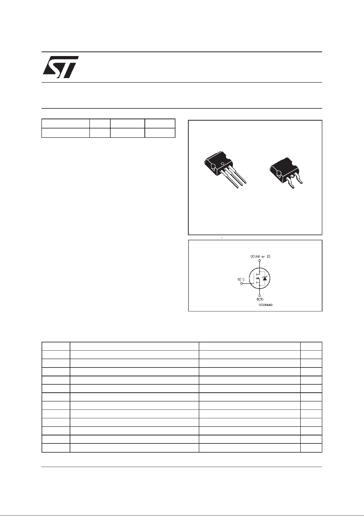
■ SURFACE-MOUNTING D
POWERPACKAGEIN TUBE (NO SUFFIX)
OR IN TAPE& REEL (SUFFIX ”T4”)
R
DS(on)
2
PAK(TO-263)
I
STB80NF10
PRELIMINARY DATA
D
3
2
1
3
1
DESCRIPTION
This MOSFET series realized with
STMicroelectronicsunique STripFETprocess has
I2PAK
TO-262
(Suffix”-1”)
D2PAK
TO-263
(Suffix”T4”)
specifically been designed to minimize input
capacitance and gate charge. It is therefore
suitable as primary switch in advanced
high-efficiency, high-frequency isolated DC-DC
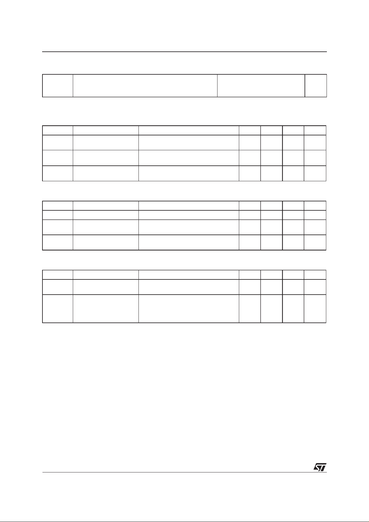
INTERNAL SCHEMATIC DIAGRAM
converters for Telecom and Computer
applications. It is also intended for any
applicationswith low gate drive requirements.
APPLICATIONS
■ HIGH-EFFICIENCYDC-DC CONVERTERS
■ UPSAND MOTORCONTROL
ABSOLUTE MAXIMUM RATINGS
Symbol Parameter Value Uni t
V
V
V
I
DM
P
dv/ dt (
E
AS
T
(•) Pulse widthlimited by safeoperating area (2) starting Tj
April 2000
Dra in- sour c e Voltage (VGS= 0) 100 V
DS
Drain- gate Voltage (RGS=20kΩ) 100 V
DGR
Gate-s ource Volt age ± 20 V
GS
Dra in Current (conti nuous) at Tc=25oC80A
I
D
Dra in Current (conti nuous) at Tc= 100oC50A
I
D
(•) Dra in Current ( puls e d) 320 A
Tot al Dissi pat io n a t Tc=25oC 210 W
tot
Der ati ng Fac t or 1.4 W/
1 ) Peak Diode Recove ry volta ge slope 9 V/ns
(2) Single Pu ls e A v alan c he Energy 245 mJ
St orage Tem pe ra t ure -65 to 175
stg
Max. Operat ing Junc tion T e m pe ra t ure 175
T
j
=25oC, ID=80A, VDD= 50V (1) ISD≤ 80 A,di/dt ≤ 300A/µs, VDD≤ V
(BR)DSS,Tj≤TJMA
o
C
o
C
o
C
1/7
Page 2
STB80NF10
THERMAL DATA
R
thj-case
R
thj-amb
T
Ther mal Resistanc e Junct ion-case Max
Ther mal Resistanc e Junct ion-ambie nt Max
Maximum L ead Tempera t ure For S o lder ing Purp os e
l
0.71
62.5
300
o
C/W
o
C/W
o
C
ELECTRICAL CHARACTERISTICS
=25oC unless otherwisespecified)
(T
case
OFF
Symbol Parameter Test Conditions Min. Typ. Max. Unit
V
(BR)DSS
Drain-source
ID=250µAVGS= 0 100 V
Break dow n Volt age
I
DSS
I
GSS
Zero Gate Voltage
Drain Current ( V
GS
Gat e- bod y L eak ag e
Current (V
DS
=0)
=0)
V
=MaxRating
DS
=MaxRating Tc=125oC
V
DS
V
= ± 20 V ± 100 nA
GS
1
10
ON(∗)
Symbol Parameter Test Conditions Min. Typ. Max. Unit
V
GS(th)
R
DS(on)
Gate Threshold Voltage VDS=VGSID= 250 µ A 234V
Sta t ic Drain -s ource On
VGS=10V ID= 40 A 0.014 0. 01 8 Ω
Resistance
I
D(on)
On State Drain Current VDS>I
D(on)xRDS(on)max
80 A
VGS=10V
DYNAMIC
Symbol Parameter Test Conditions Min. Typ. Max. Unit
g
(∗)Forward
fs
Tr ansc on duc tance
C
C
C
Input C apacitance
iss
Out put Capacitance
oss
Reverse Tr ansfer
rss
Capacit a nc e
VDS>I
D(on)xRDS(on)maxID
=40 A 20 S
VDS=25V f=1MHz VGS= 0 4300
600
240
µA
µ
pF
pF
pF
A
2/7
Page 3
STB80NF10
ELECTRICAL CHARACTERISTICS
(continued)
SWITCHING ON
Symbol Parameter Test Conditions Min. Typ. Max. Unit
t
d(on)
Tur n-on Delay Time
Rise Ti m e
t
r
VDD=50V ID=40A
R
=4.7
G
Ω
VGS=10V
40
145
(Resis t iv e Loa d, see fig. 3)
Q
Q
Q
Tot al G at e Charge
g
Gat e- Source Char g e
gs
Gate-Drain Charge
gd
VDD=80V ID=80A VGS= 10 V 140
23
51
SWITCHING OFF
Symbol Parameter Test Conditions Min. Typ. Max. Unit
t
d(off)
Tur n-of f D ela y Time
t
Fall T ime
f
VDD=27V ID=40A
=4.7 Ω VGS=10V
R
G
134
115
(Resis t iv e Loa d, see fig. 3)
t
d(off)
Off-voltage Rise Time
t
Fall T ime
f
t
Cross-over Tim e
c
Vclamp = 80 V ID=80A
=4.7 Ω VGS=10V
R
G
(Indu ct iv e Load, se e fig. 5)
111
125
185
SOURCEDRAINDIODE
Symbol Parameter Test Conditions Min. Typ. Max. Unit
I
SD
I
SDM
V
SD
t
Q
I
RRM
(∗)Pulsed: Pulse duration =300 µs, duty cycle1.5 %
(•) Pulse width limitedby safe operatingarea
Source-drain Current
(•)
Source-drain Current
80
320
(pulsed)
(∗)ForwardOnVoltage ISD=80A VGS=0 1.5 V
Reverse Recover y
rr
Time
Reverse Recover y
rr
ISD= 80 A di/dt = 100 A/µs
=50V Tj=150oC
V
DD
(see test circuit, fig. 5)
155
850
Charge
Reverse Recover y
11
Current
ns
ns
nC
nC
nC
ns
ns
ns
ns
ns
A
A
ns
nC
A
3/7
Page 4

STB80NF10
Fig. 1
: UnclampedInductive Load Test Circuit
Fig. 3: Switching Times Test Circuits For
ResistiveLoad
Fig. 2
: UnclampedInductiveWaveform
Fig. 4: Gate Charge test Circuit
Fig. 5
: Test Circuit For Inductive Load Switching
And Diode Recovery Times
4/7
Page 5

TO-262 (I2PAK) MECHANICAL DATA
STB80NF10
DIM.
MIN. TYP. MAX. MIN. TYP. MAX.
A 4.4 4.6 0.173 0.181
A1 2.49 2.69 0.098 0.106
B 0.7 0.93 0.027 0.036
B2 1.14 1.7 0.044 0.067
C 0.45 0.6 0.017 0.023
C2 1.23 1.36 0.048 0.053
D 8.95 9.35 0.352 0.368
e 2.4 2.7 0.094 0.106
E 10 10.4 0.393 0.409
L 13.1 13.6 0.515 0.531
L1 3.48 3.78 0.137 0.149
L2 1.27 1.4 0.050 0.055
mm inch
CA1
A
C2
B2
B
e
E
L1
L2
D
L
P011P5/E
5/7
Page 6

STB80NF10
TO-263 (D2PAK) MECHANICAL DATA
DIM.
MIN. TYP. MAX. MIN. TYP. MAX.
A 4.4 4.6 0.173 0.181
A1 2.49 2.69 0.098 0.106
B 0.7 0.93 0.027 0.036
B2 1.14 1.7 0.044 0.067
C 0.45 0.6 0.017 0.023
C2 1.21 1.36 0.047 0.053
D 8.95 9.35 0.352 0.368
E 10 10.4 0.393 0.409
G 4.88 5.28 0.192 0.208
L 15 15.85 0.590 0.624
L2 1.27 1.4 0.050 0.055
L3 1.4 1.75 0.055 0.068
mm inch
6/7
D
A
C2
DETAIL”A”
C
A2
DETAIL”A”
A1
B2
E
L2
L
L3
B
G
P011P6/E
Page 7

STB80NF10
Information furnished is believed to be accurate and reliable. However, STMicroelectronics assumes no responsibility for the consequences
of use of such information nor for any infringement of patents or other rights of third parties which may result from its use. No license is
granted by implication or otherwise under any patent or patent rights of STMicroelectronics. Specification mentioned in this publication are
subject to change without notice. This publication supersedes and replaces all information previously supplied. STMicroelectronics products
are not authorized for use as critical components in life support devices or systems without express written approval of STMicroelectronics.
The ST logo is a trademarkof STMicroelectronics
2000 STMicroelectronics – Printed in Italy – All Rights Reserved
STMicroelectronics GROUP OF COMPANIES
Australia - Brazil -China - Finland- France- Germany - Hong Kong - India - Italy - Japan - Malaysia - Malta -Morocco -
Singapore - Spain - Sweden -Switzerland - United Kingdom - U.S.A.
http://www.st.com
7/7
 Loading...