

Page 1
STB80NF03L-04
N-CHANNEL 30V - 0.0035
TYPE V
DSS
ST B80NF03L- 04 30 V < 0. 004 Ω 80 A
■ TYPICALR
■ EXCEPTIONALdv/dtCAPABILITY
■ 100%AVALANCHETESTED
■ LOW THRESHOLDDRIVE
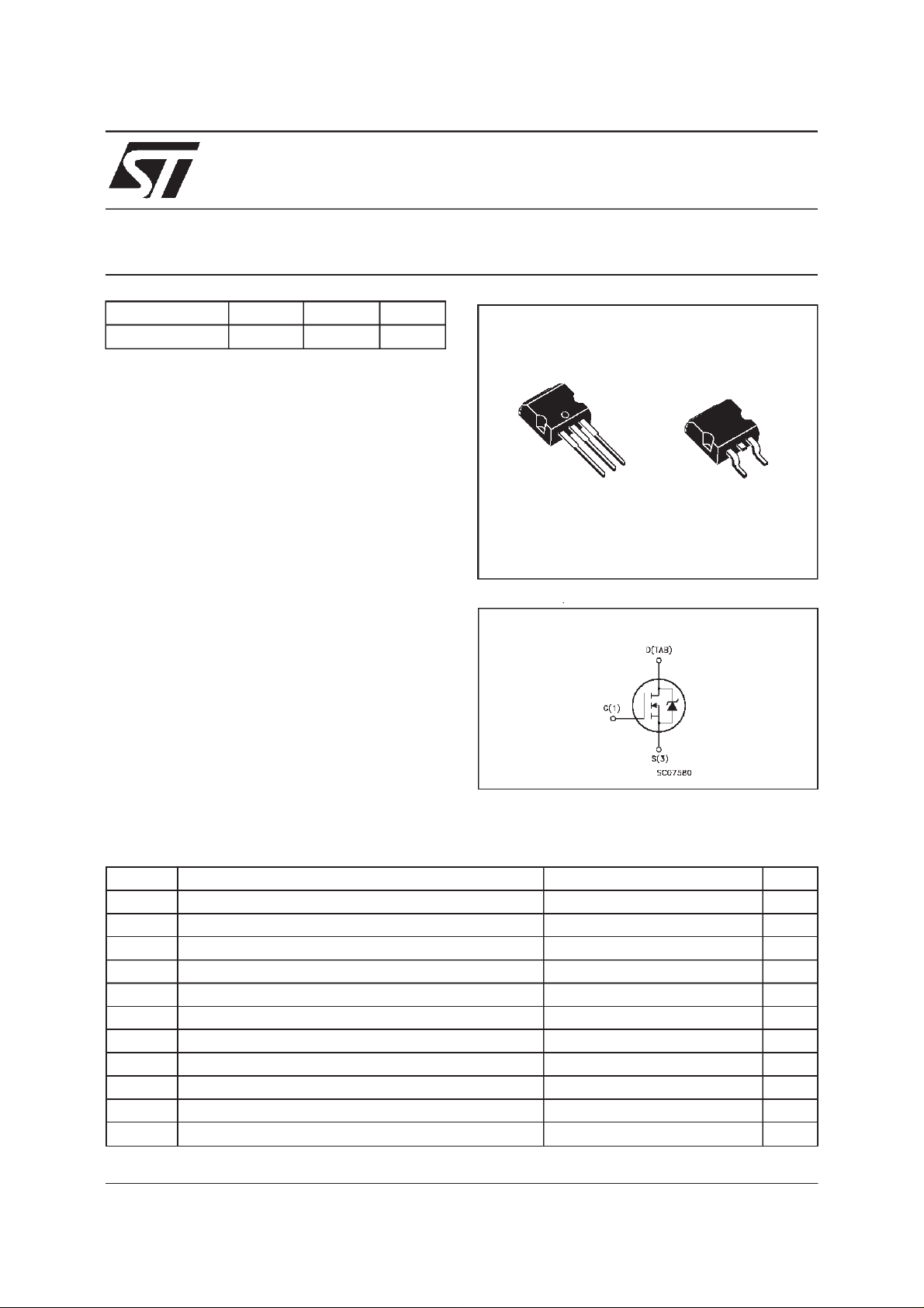
■ THROUGH-HOLE I2PAK (TO-262) POWER
DS(on)
= 0.0035 Ω
PACKAGEIN TUBE(SUFFIX ”-1”)
■ SURFACE-MOUNTINGD2PAK (TO-263)
POWERPACKAGEIN TUBE (NO SUFFIX)
OR IN TAPE& REEL (SUFFIX ”T4”)
DESCRIPTION
This Power Mosfet is the latest development of
STMicroelectronics unique ”Single Feature
Size” strip-based process. The resulting
transistor shows extremely high packing density
for low on-resistance, rugged avalanche
characteristics and less critical alignment steps
therefore a remarkable manufacturing
reproducibility.
R
DS(on)
I
D
Ω
- 80A TO-262/TO-263
STripFET POWER MOSFET
PRELIMINARY DATA
3
2
1
I2PAK
TO-262
(suffix”-1”)
D2PAK
TO-263
(suffix”T4”)
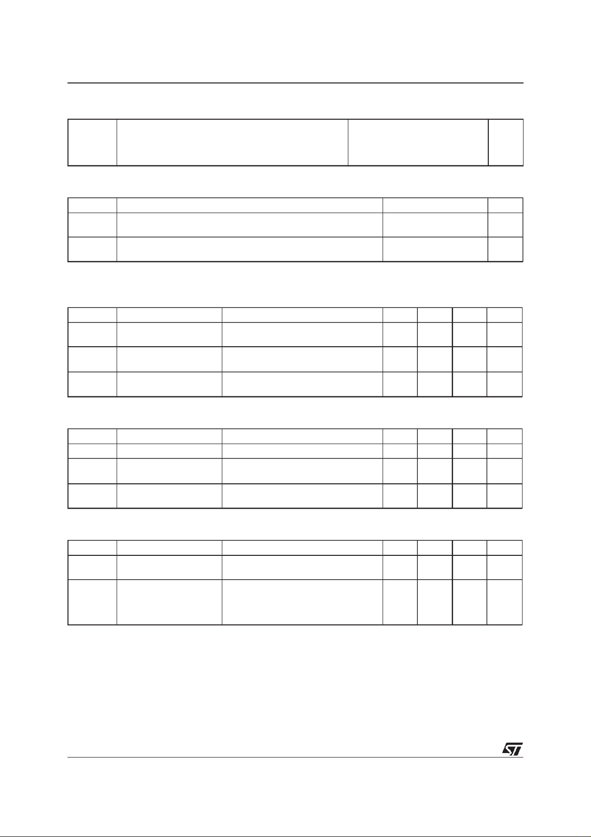
INTERNAL SCHEMATIC DIAGRAM
3
1
APPLICATIONS
■ HIGHCURRENT, HIGH SPEEDSWITCHING
■ MOTORCONTROL, AUDIOAMPLIFIERS
■ DC-DC& DC-AC CONVERTERS
■ AUTOMOTIVEENVIRONMENT(INJECTION,
ABS, AIR-BAG, LAMPDRIVERS,Etc. )
ABSOLUTE MAXIMUM RATINGS
Symbol Parameter Value Unit
V
V
V
I
DM
P
dv/ dt Peak Diode Re c overy volt age sl ope 3.5 V/ns
T
(•) Pulse width limited by safe operating area (1)ISD≤ 80 A, di/dt ≤ 300 A/µs, VDD≤ V
March 2000
Dra in- sour c e Volt age ( VGS=0) 30 V
DS
Dra in- gat e Vol tage ( RGS=20kΩ)30V
DGR
Gat e-source V oltage
GS
I
Dra in Cu rr ent (c ontinuous) a t Tc=25oC80A
D
I
Dra in Cu rr ent (c ontinuous) a t Tc=100oC56A
D
20 V
±
(•) D rain Curr ent (pulsed ) 320 A
Tot al Dissipation at Tc=25oC 210 W
tot
Der ati ng Fac t or 1.43 W/
St orage Tempe r at ur e -65 to 175
stg
T
Max. O per at ing J unc t ion T emper at ure 175
j
(BR)DSS,Tj≤TJMAX
o
C
o
C
o
C
1/7
Page 2
STB80NF03L-04
THERMAL DATA
R
thj-case
Rthj-a mb
R
thc-sink
T
AVALANCHE CHARACTERISTICS
Symbol Parameter Max Value Unit
I
AR
E
Ther mal Resistanc e Junct ion-case Max
Ther mal Resistanc e Junct ion-ambie nt Max
Ther mal Resistanc e Case-sink Ty p
Maximum Lead Tem pe ra t ure For So ldering Purp ose
l
Avalanche Current, Repetitive or Not-Repetiti ve
(pulse width limited by T
Single Pul s e Avalan che Energy
AS
(starting T
=25oC, ID=IAR,VDD=15V)
j
max)
j
0.7
62.5
0.5
300
80 A
600 mJ
o
C/W
oC/W
o
C/W
o
C
ELECTRICAL CHARACTERISTICS
=25oC unless otherwisespecified)
(T
case
OFF
Symbol Parameter Test Condit ions Min. Typ. Max. Unit
V
(BR)DSS
Drain-source
ID=250µAVGS=0 30 V
Break dow n Voltage
I
DSS
I
GSS
Zero Gate Volta ge
Drain Curr e nt (V
GS
Gat e- bod y Leak ag e
Current (V
DS
=0)
=0)
V
=MaxRating
DS
=MaxRating Tc=125oC
V
DS
V
=± 20 V
GS
1
10
100 nA
±
ON(∗)
Symbol Parameter Test Condit ions Min. Typ. Max. Unit
V
GS(th)
R
DS(on)
I
D(on)
Gate Threshold Voltage VDS=VGSID= 250 µA11.52.5V
Sta t ic Drain-s ource On
Resistance
VGS=10V ID=40A
=4.5V ID=40A
V
GS
On State Drain Current VDS>I
D(on)xRDS(on)max
0.0035
0.004
80 A
0.004
0.0055ΩΩ
VGS=10V
DYNAMIC
Symbol Parameter Test Condit ions Min. Typ. Max. Unit
g
(∗)Forward
fs
Tr ansc on duc tance
C
C
C
Input Capaci t anc e
iss
Out put Capac it ance
oss
Reverse Tr ansfer
rss
Capacit a nc e
VDS>I
D(on)xRDS(on)maxID
=15 A 20 50 S
VDS=25V f=1MHz VGS= 0 7000
1700
600
µ
µA
pF
pF
pF
A
2/7
Page 3
STB80NF03L-04
ELECTRICAL CHARACTERISTICS
(continued)
SWITCHING ON
Symbol Parameter Test Condit ions Min. Typ. Max. Unit
t
d(on)
t
Tur n-on Delay Tim e
Rise Tim e
r
VDD=15V ID=40A
R
=4.7
G
Ω
VGS=4.5V
50
230
(Resis t iv e Load, s ee fig. 3 )
Q
Q
Q
Tot al Gate Charge
g
Gat e- Source Charg e
gs
Gate-Drain Charge
gd
VDD=24V ID=80A VGS= 4.5 V 100
22
42
135 nC
SWITCHING OFF
Symbol Parameter Test Condit ions Min. Typ. Max. Unit
t
d(off)
Tur n-of f Dela y Time
t
Fall T ime
f
VDD=15V ID=40A
=4.7 Ω VGS=4.5V
R
G
220
130
(Resis t iv e Load, s ee fig. 3 )
t
r(Voff)
t
t
Off-voltage Rise Time
Fall T ime
f
Cross-over T ime
c
V
=24V ID=80A
clamp
=4.7 Ω VGS=4.5V
R
G
(Indu ct iv e Load , se e fig. 5)
65
250
340
SOURCEDRAINDIODE
Symbol Parameter Test Condit ions Min. Typ. Max. Unit
I
SDM
V
I
SD
Q
I
RRM
SD
t
Source-drain Current
(•)
Source-drain Current
80
320
(pulsed)
(∗)ForwardOnVoltage ISD=80A VGS=0 1.5 V
Reverse Recovery
rr
Time
Reverse Recovery
rr
ISD= 80 A di/dt = 100 A/µs
=15V Tj=150oC
V
DD
(see test circuit, fig. 5)
70
0.14
Charge
Reverse Recovery
4
Current
ns
ns
nC
nC
ns
ns
ns
ns
ns
A
A
ns
µC
A
(∗) Pulsed: Pulse duration = 300 µs, duty cycle 1.5%
(•) Pulse width limited by safe operatingarea
3/7
Page 4

STB80NF03L-04
Fig. 1:
UnclampedInductiveLoad Test Circuit
Fig. 3: SwitchingTimes Test Circuits For
ResistiveLoad
Fig. 2:
UnclampedInductive Waveform
Fig. 4: Gate Chargetest Circuit
Fig. 5:
Test CircuitFor InductiveLoad Switching
And Diode Recovery Times
4/7
Page 5

TO-262 (I2PAK) MECHANICAL DATA
STB80NF03L-04
DIM.
MIN. TYP. MAX. MIN. TYP. MAX.
A 4.4 4.6 0.173 0.181
A1 2.49 2.69 0.098 0.106
B 0.7 0.93 0.027 0.036
B2 1.14 1.7 0.044 0.067
C 0.45 0.6 0.017 0.023
C2 1.23 1.36 0.048 0.053
D 8.95 9.35 0.352 0.368
e 2.4 2.7 0.094 0.106
E 10 10.4 0.393 0.409
L 13.1 13.6 0.515 0.531
L1 3.48 3.78 0.137 0.149
L2 1.27 1.4 0.050 0.055
mm inch
CA1
A
C2
B2
B
e
E
L1
L2
D
L
P011P5/E
5/7
Page 6

STB80NF03L-04
TO-263 (D2PAK) MECHANICAL DATA
DIM.
MIN. TYP. MAX. MIN. TYP. MAX.
A 4.4 4.6 0.173 0.181
A1 2.49 2.69 0.098 0.106
B 0.7 0.93 0.027 0.036
B2 1.14 1.7 0.044 0.067
C 0.45 0.6 0.017 0.023
C2 1.21 1.36 0.047 0.053
D 8.95 9.35 0.352 0.368
E 10 10.4 0.393 0.409
G 4.88 5.28 0.192 0.208
L 15 15.85 0.590 0.624
L2 1.27 1.4 0.050 0.055
L3 1.4 1.75 0.055 0.068
mm inch
6/7
D
A
C2
DETAIL”A”
C
A2
DETAIL”A”
A1
B2
E
L2
L
L3
B
G
P011P6/E
Page 7

STB80NF03L-04
Information furnishedis believed tobe accurateand reliable. However, STMicroelectronics assumes no responsibilityforthe consequences
of use of such information nor for any infringement of patents or other rights of third parties which may result from its use. No license is
granted by implication or otherwise under any patent or patent rights of STMicroelectronics. Specificationmentioned in this publication are
subjecttochange without notice. This publication supersedes and replaces all information previously supplied. STMicroelectronicsproducts
are not authorized for use as critical components in life support devices or systemswithout express written approval of STMicroelectronics.
The STlogo is a trademark of STMicroelectronics
1999 STMicroelectronics – Printed in Italy – All Rights Reserved
STMicroelectronics GROUP OF COMPANIES
Australia - Brazil - China - Finland - France - Germany - Hong Kong - India - Italy - Japan - Malaysia - Malta - Morocco -
Singapore - Spain - Sweden - Switzerland - United Kingdom - U.S.A.
http://www.st.com
.
7/7
 Loading...