

Page 1
STB80NE03L-06
STB80NE03L-06-1
N-CHANNEL 30V - 0.005Ω -80AD2PAK / I2PAK
STripFET™ PO WE R MOSFET
TYPE V
STB80NE03L-06
STB80NE03L-06-1
■ TYPICAL R
■ EXCEPTIONAL dv/dt CAPABILITY
■ LOW GATE CHARGE 100°C
■ 100% AVALANCHE TES TED
(on) = 0.005 Ω
DS
DSS
30 V
30 V
R
DS(on)
< 0.006 Ω
< 0.006 Ω
I
D
80 A
80 A
DESCRIPTION
This Power MOSFET is the latest development of
STMicroelectronics unique “Single Feature
Size™” strip-based process. The resulting transistor shows extremely high packing density for low
on-resistance, rugged avalanche characteristics
and less critical alignment steps therefore a remarkable manufacturing reproducibility.
APPLICATIONS
■ HIGH CURRENT, HIGH SPEED SWITCHING
■ SOLENOID AND RELAY DRIVERS
■ MOTOR CONTROL,AUDIO AMPLIFIERS
■ DC-DC & DC-AC CONVERTERS
■ AUTOMOTIVE ENVIRONMENT (INJECTION,
ABS, AIR-BAG, LAMPDRIVERS, Etc.)
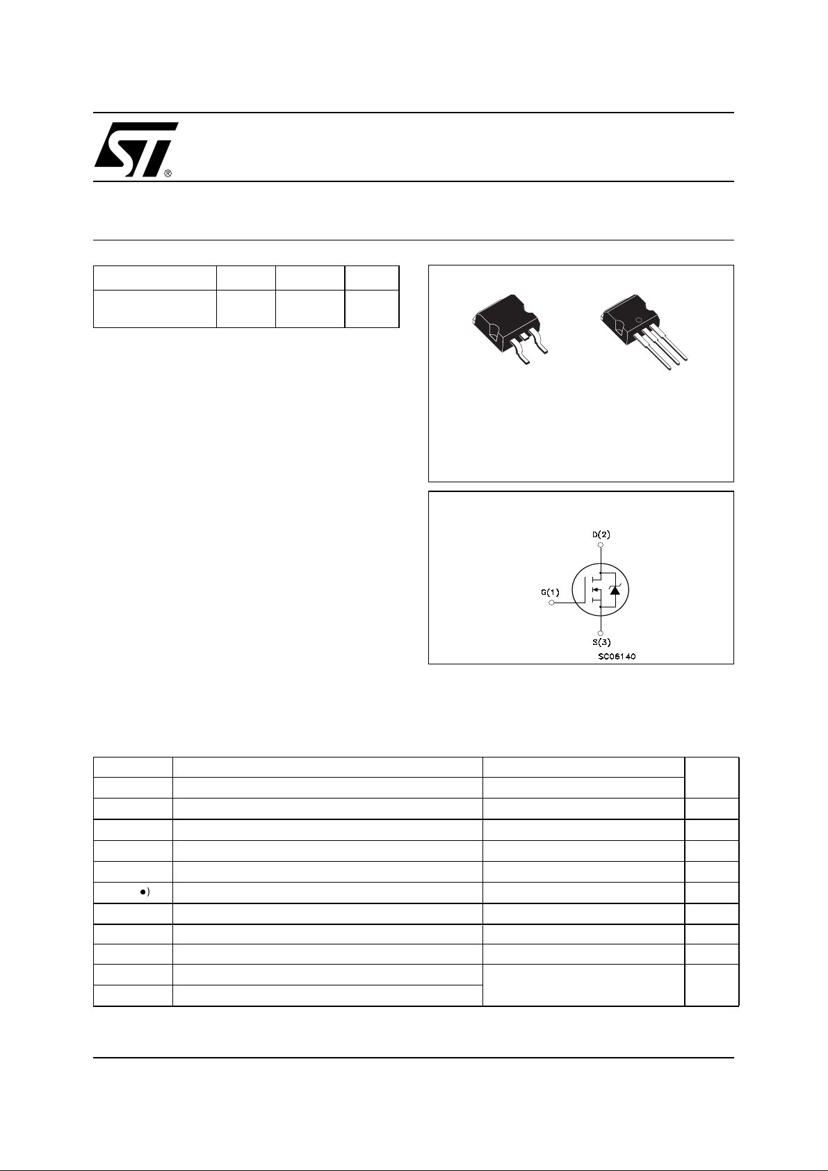
1
D2PAK
3
I2PAK
3
2
1
INTERNAL SCHEMATIC DIAGRAM
ABSOLUTE MAXIMUM RATINGS
Symbol Parameter Value Unit
V
DS
V
DGR
V
GS
I
D
I
D
I
DM
P
TOT
dv/dt (1) Peak Diode Recovery voltage slope 7 V/ns
T
stg
T
j
(●) Pulse width limited by safe operating area
Drain-source Voltage (VGS=0)
Drain-gate Voltage (RGS=20kΩ)
30 V
30 V
Gate- source Voltage ± 20 V
Drain Current (continuos) at TC= 25°C
Drain Current (continuos) at TC= 100°C
()
Drain Current (pulsed) 320 A
Total Dissipation at TC= 25°C
80 A
60 A
150 W
Derating Factor 1 W/°C
Storage Temperature
Max. Operating Junction Temperature
(1) ISD≤804A, di/dt ≤300A/µs, VDD≤ V
–55to175 °C
(BR)DSS,Tj≤TJMAX.
1/9February 2003
Page 2
STB80NE03L-06 / STB80NE03L- 06-1
THERMAL DATA
Rthj-case Thermal Resistance Junction-case Max 1 °C/W
Rthj-amb Thermal Resistance Junction-ambient Max 62.5 °C/W
T
l
AVALANCHE CHARACTERISTICS
Symbol Parameter Max Value Unit
I
AR
E
AS
ELECTRICAL CHARACTERISTICS (TCASE = 25 °C UNLESS OTHERWISE SPECIFIED)
OFF
Symbol Parameter Test Conditions Min. Typ. Max. Unit
V
(BR)DSS
I
DSS
I
GSS
Maximum Lead Temperature For Soldering Purpose 300 °C
Avalanche Current, Repetitive or Not-Repetitive
(pulse width limited by T
max)
j
Single Pulse Avalanche Energy
(starting T
Drain-source
= 25 °C, ID=IAR,VDD=15V)
j
ID= 250 µA, VGS= 0 30 V
80 A
600 mJ
Breakdown Voltage
Zero Gate Voltage
Drain Current (V
GS
Gate-body Leakage
Current (V
DS
=0)
=0)
V
= Max Rating
DS
= Max Rating, TC= 125 °C
V
DS
V
= ± 20 V ± 100 nA
GS
1µA
10 µA
ON (1)
Symbol Parameter Test Conditions Min. Typ. Max. Unit
V
GS(th)
R
DS(on)
Gate Threshold Voltage
Static Drain-source On
Resistance
V
DS=VGS,ID
VGS=10V,ID=40A
= 4.5 V, ID=40A
V
GS
= 250µA
1 1.7 2.5 V
0.005 0.006 Ω
0.008 Ω
DYNAMIC
Symbol Parameter Test Conditions Min. Typ. Max. Unit
(1) Forward Transconductance VDS>I
g
fs
C
iss
C
oss
C
rss
Input Capacitance
Output Capacitance 1500 pF
Reverse Transfer
Capacitance
D(on)xRDS(on)max,
ID=40A
V
=25V,f=1MHz,VGS=0
DS
30 50 S
6500 pF
500 pF
2/9
Page 3
STB80NE03L-06 / STB80NE03L -06-1
ELECTRICAL CHARACTERISTICS (CONTINUED)
SWITCHING ON
Symbol Parameter Test Conditions Min. Typ. Max. Unit
V
t
d(on)
Q
Q
Q
t
r
g
gs
gd
Turn-on Delay Time
Rise Time 260 350 ns
Total Gate Charge
Gate-Source Charge
Gate-Drain Charge
SWITCHING OFF
Symbol Parameter Test Conditions Min. Typ. Max. Unit
t
r(Voff)
t
t
f
c
Off-voltage Rise Time
Fall Time
Cross-over Time
SOURCE DRAIN DIODE
Symbol Parameter Test Conditions Min. Typ. Max. Unit
I
SD
I
SDM
VSD(1)
t
rr
Q
rr
I
RRM
Note: 1. Pulsed: Pulse duration = 300 µs, duty cycle 1.5 %.
2. Pulse width limited by safe operating area.
Source-drain Current 80 A
(2)
Source-drain Current (pulsed) 320 A
Forward On Voltage
Reverse Recovery Time
Reverse Recovery Charge
Reverse Recovery Current
=15V,ID=40A
DD
= 4.7Ω VGS=4.5V
R
G
(see test circuit, Figure 3)
=24V,ID= 80A,
V
DD
V
=5V
GS
=24V,ID=80A,
V
DD
=4.7Ω, VGS=5V
R
G
(see test circuit, Figure 3)
ISD=80A,VGS=0
= 80 A, di/dt = 100A/µs,
I
SD
VDD=15V,Tj= 150°C
(see test circuit, Figure 5)
40 55 ns
95
130 nC
30
44
70
165
250
95
220
340
1.5 V
75
0.14
4
nC
nC
ns
ns
ns
ns
nC
A
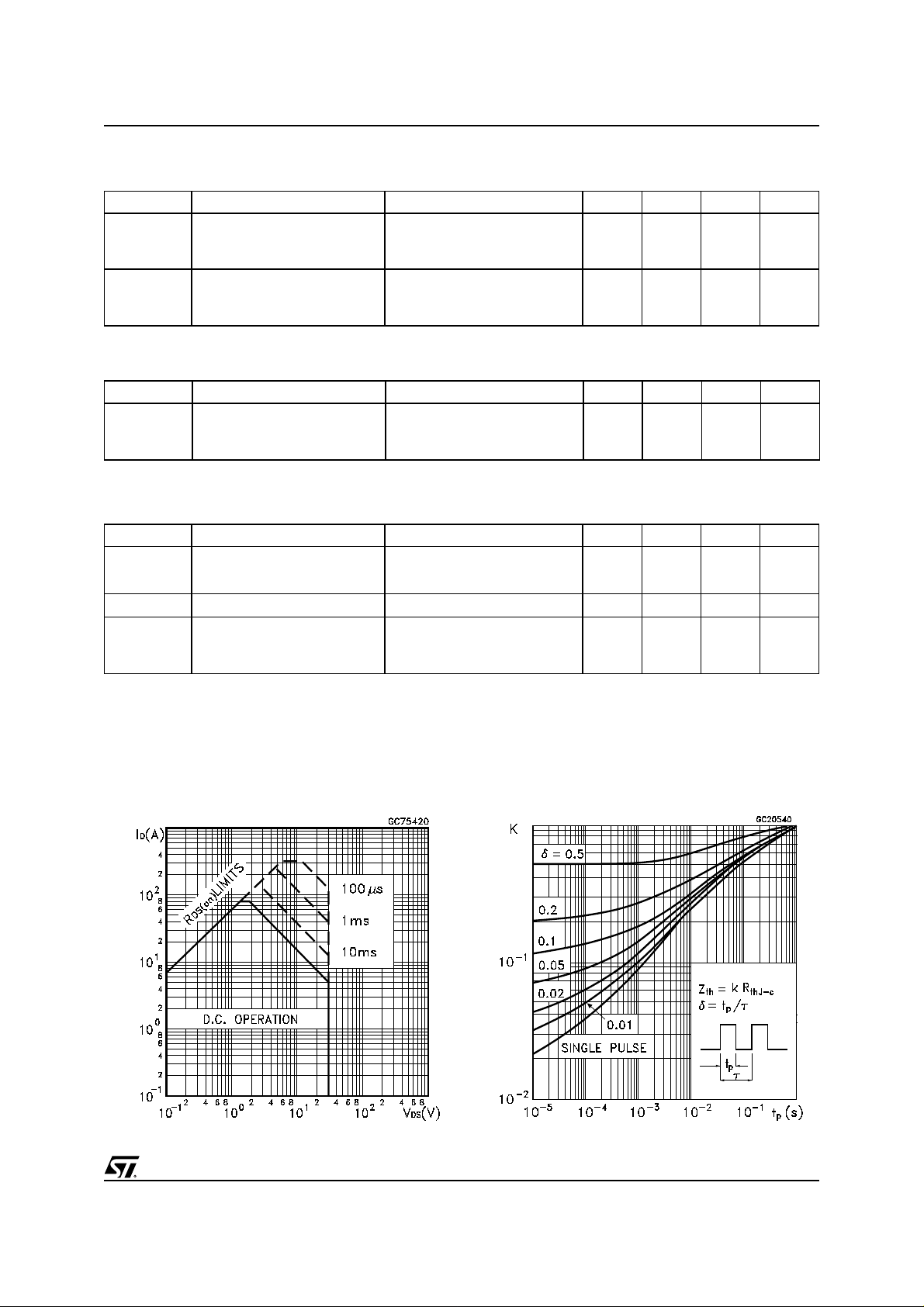
Safe Operating Area Thermal Impedence
3/9
Page 4

STB80NE03L-06 / STB80NE03L- 06-1
Output Characteristics
Transfer Characteristics
Static Drain-source On ResistanceTransconductance
Gate Charge vs Gate-so urce Voltage
4/9
Capacitance Variations
Page 5

STB80NE03L-06 / STB80NE03L -06-1
Normalized Gate Threshold Voltage vs
Temperature
Source-drain Diode Forward Characteristics
Normalized On Resistance vs Temperature
5/9
Page 6

STB80NE03L-06 / STB80NE03L- 06-1
Fig. 2: Unclamped Induc tive WaveformFig. 1: Unclamped Inductive Load Test C ircuit
Fig. 3: Switching Times Tes t Circuit For
Resistive Load
Fig. 5: Test Circuit For Inductive Load Switching
And Diode Recovery Times
Fig. 4: Gate Charge test Circuit
6/9
Page 7

STB80NE03L-06 / STB80NE03L -06-1
D2PAK MECHANICAL DATA
DIM.
MIN. TYP MAX. MIN. TYP. MAX.
A 4.4 4.6 0.173 0.181
A1 2.49 2.69 0.098 0.106
A2 0.03 0.23 0.001 0.009
B 0.7 0.93 0.027 0.036
B2 1.14 1.7 0.044 0.067
C 0.45 0.6 0.017 0.023
C2 1.23 1.36 0.048 0.053
D 8.95 9.35 0.352 0.368
D1 8 0.315
E 10 10.4 0.393
E1 8.5 0.334
G 4.88 5.28 0.192 0.208
L 15 15.85 0.590 0.625
L2 1.27 1.4 0.050 0.055
L3 1.4 1.75 0.055 0.068
mm. inch
M 2.4 3.2 0.094 0.126
R 0.4 0.015
V2 0º 8º
3
7/9
1
Page 8

STB80NE03L-06 / STB80NE03L- 06-1
TO-262 (I2PAK) MECHANICAL DATA
DIM.
MIN. TYP. MAX. MIN. TYP. MAX.
A 4.4 4.6 0.173 0.181
A1 2.49 2.69 0.098 0.106
B 0.7 0.93 0.027 0.036
B2 1.14 1.7 0.044 0.067
C 0.45 0.6 0.017 0.023
C2 1.23 1.36 0.048 0.053
D 8.95 9.35 0.352 0.368
e 2.4 2.7 0.094 0.106
E 10 10.4 0.393 0.409
L 13.1 13.6 0.515 0.531
L1 3.48 3.78 0.137 0.149
L2 1.27 1.4 0.050 0.055
mm inch
C
8/9
A
A1
C2
B2
B
e
E
L1
L2
D
L
P011P5/E
Page 9

STB80NE03L-06 / STB80NE03L -06-1
Information furnished is believed to be accurate and reliable. However, STMicroelectronics assumes no responsibility for the
consequences of u se of such inform ation nor for any in fring ement of p atents or o ther ri ghts of th ird p arties which may r esul t f rom
its use. No license is granted by implication or otherwise under any patent or patent rights of STMicroelectronics. Specifications
mentioned in this publication are subject to change without notice. This publication supersedes and replaces all information
previously supplied. STMicroelectronics products are not authorized for use as critical components in life support devices or
systems without express written approval of STMicroelectronics.
Australia - Brazil - Canada - China - Finland - France - Germany - Hong Kong - India - Israel - Italy - Japan - Malaysia - Malta - Morocco
© The ST logo is a registered trademark of STMicroelectronics
© 2003 STMicroelectronics - Printed in Italy - All Rights Reserved
Singapore - Spain - Sweden - Switzerland - United Kingdom - United States.
STMicroelectronics GROUP OF COMPANIES
© http://www.st.com
9/9
 Loading...