

Page 1
STB7NB60
N - CHANNEL 600V - 1.0 OMH - 7.2A - I2PAK/D2PAK
PowerMESH MOSFET
TYPE V
DSS
R
DS(on)
I
D
STB7NB60 600 V < 1.2 Ω 7.2 A
■ TYPICALR
■ EXTREMELY HIGH dv/dt CAPABILITY
■ 100% AVALANCHETESTED
■ VERYLOW INTRINSIC CAPACITANCES
■ GATECHARGEMINIMIZED
DS(on)
=1.0 Ω
DESCRIPTION
Using the latest high voltage MESH OVERLAY
process, SGS-Thomson has designed an
advanced family of power MOSFETs with
outstanding performances. The new patent
pending strip layout coupled with the Company’s
proprietary edge termination structure, gives the
lowest RDS(on) per area, exceptional avalanche
and dv/dt capabilities and unrivalled gate charge
and switching characteristics.
APPLICATIONS
■ HIGH CURRENT, HIGH SPEEDSWITCHING
■ SWITCHMODEPOWER SUPPLIES(SMPS)
■ DC-ACCONVERTERS FOR WELDING
EQUIPMENTAND UNINTERRUPTIBLE
POWERSUPPLIESAND MOTORDRIVE
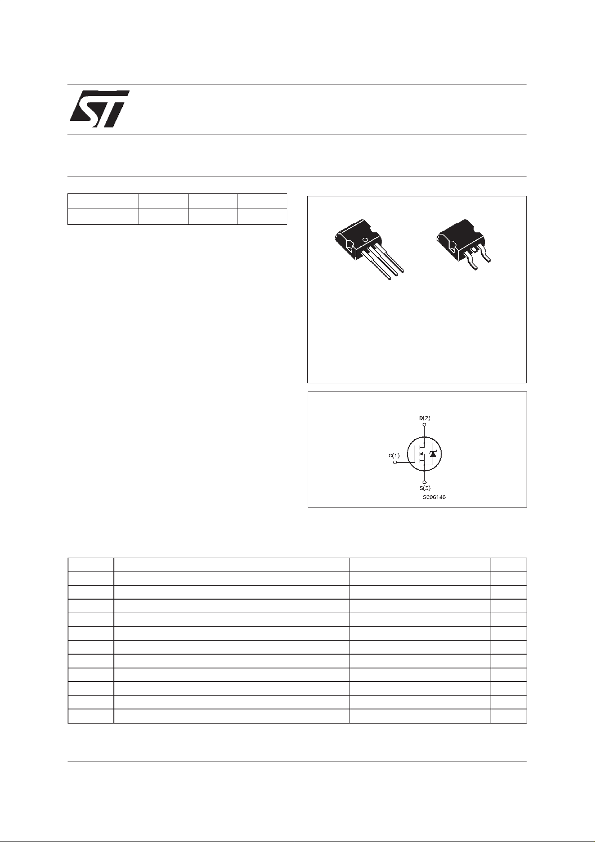
3
1
I2PAK
TO-262
(suffix ”-1”)
3
2
1
D2PAK
TO-252
(Suffix ”T4”)
INTERNAL SCHEMATIC DIAGRAM
ABSOLUTE MAXIMUM RATINGS
Symb o l Para meter Value Uni t
V
V
V
I
DM
P
dv/dt(
T
(•) Pulse width limited by safe operating area (1)ISD≤ 7A, di/dt ≤ 200 A/µs, VDD≤ V
June 1998
Drain-source Voltage (VGS=0) 600 V
DS
Drain- gate Voltage ( RGS=20kΩ)
DGR
Gat e- source Vo lt age ± 30 V
GS
Drain Cur rent ( continuous) at Tc=25oC7.2A
I
D
Drain Cur rent ( continuous) at Tc=100oC4.5A
I
D
600 V
(•) Dra in C urr ent (pulsed) 28.8 A
Tot al Dissipation at Tc=25oC125W
tot
Derating Factor 1.0 W/
1) Peak Diode Rec overy volt age s l ope 4.5 V/ns
Sto rage Tempe rature -65 to 150
stg
Max. Operating Ju nc t io n Tem peratur e 150
T
j
,Tj≤T
(BR)DSS
JMAX
o
C
o
C
o
C
1/8
Page 2
STB7NB60
THERMAL DATA
R
thj-case
Rthj-a mb
R
thc-sin k
T
AVALANCHE CHARACTERISTICS
Symbol Para met e r Max Value Uni t
I
AR
E
Ther mal Resist ance Junctio n-c a se Max
Ther mal Resist ance Junctio n-ambient Max
Ther mal Resist ance Case-sink T yp
Maximum Lead Temperat u re F o r Soldering Purp ose
l
Avalanche Cur rent, Rep etit ive or Not-Re petitive
(pulse width limited by T
Single Pulse Avalanche Energy
AS
(starting T
=25oC, ID=IAR,VDD=50V)
j
max, δ <1%)
j
1.0
62.5
0.5
300
7.2 A
580 mJ
o
C/W
oC/W
o
C/W
o
C
ELECTRICAL CHARACTERISTICS (T
=25oC unlessotherwise specified)
case
OFF
Symbol Parameter Test Cond itions Min. Typ. M ax. Unit
V
(BR)DSS
Drain-sourc e
=250µAVGS=0
I
D
600 V
Breakdown V oltage
I
DSS
I
GSS
Zer o Gat e V o lt age
Drain Current (V
GS
Gat e-body Leaka ge
Current (V
DS
=0)
=0)
=MaxRating
V
DS
V
=MaxRating Tc=125oC
DS
= ± 30 V
V
GS
1
50
± 100 nA
ON (∗)
Symbol Parameter Test Cond itions Min. Typ. M ax. Unit
V
GS(th )
Gate Threshold
V
DS=VGSID
=250µA
345V
Voltage
R
DS(on)
Stati c D rain-source On
VGS=10V ID= 3.6 A 1.0 1.2 Ω
Resistance
I
D(on)
On State Drain Curre nt VDS>I
D(on)xRDS(on)max
7.2 A
VGS=10V
DYNAMIC
Symbol Parameter Test Cond itions Min. Typ. M ax. Unit
g
(∗)Forward
fs
Tr ansconductanc e
C
C
C
Input Capac i t an c e
iss
Out put C apa c itance
oss
Reverse Transf er
rss
Capa cit an c e
VDS>I
D(on)xRDS(on)maxID
=3.6A 4 5.3 S
VDS=25V f=1MHz VGS= 0 1250
165
16
1625
223
22
µA
µA
pF
pF
pF
2/8
Page 3
STB7NB60
ELECTRICAL CHARACTERISTICS (continued)
SWITCHINGON
Symbol Parameter Test Cond itions Min. Typ. M ax. Unit
t
d(on)
Turn-on Time
r
Rise Time
t
VDD=300V ID=3.6A
=4.7 Ω VGS=10V
R
G
18
8
(see test circuit, figure 3)
Q
Q
Q
Total Gate Charge
g
Gat e-Sour ce Cha rge
gs
Gate-Drain Charge
gd
VDD=480V ID=7.2A VGS=10V 30
9.9
13.3
SWITCHINGOFF
Symbol Parameter Test Cond itions Min. Typ. M ax. Unit
t
r(Voff)
t
t
Of f - voltage Rise Time
Fall Time
f
Cross-ov er Time
c
VDD=480V ID=7.2A
=4.7 Ω VGS=10V
R
G
(see test circuit, figure 5)
8
5
15
SOURCE DRAIN DIODE
Symbol Parameter Test Cond itions Min. Typ. M ax. Unit
I
SD
I
SDM
V
SD
t
Q
I
RRM
(∗) Pulsed: Pulse duration =300 µs, duty cycle1.5 %
(•) Pulse width limited by safe operating area
Source-drain Curre nt
(•)
Source-drain Curre nt
(pulsed)
(∗) For ward On Vo ltage ISD=7.2A VGS=0 1.6 V
Reverse Recov er y
rr
Time
Reverse Recov er y
rr
= 7.2 A di/dt = 100 A /µs
I
SD
=100V Tj=150oC
V
DD
(see test circuit, figure 5)
530
4.5
Charge
Reverse Recov er y
17
Current
27
12
45 n C
12
8
23
7.2
28.8
ns
ns
nC
nC
ns
ns
ns
A
A
ns
µC
A
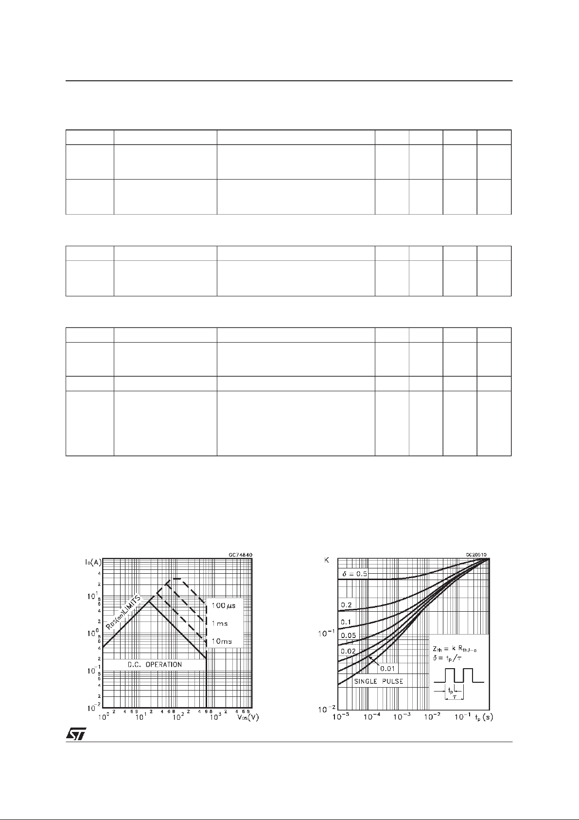
Safe Operating Area ThermalImpedance
3/8
Page 4
STB7NB60
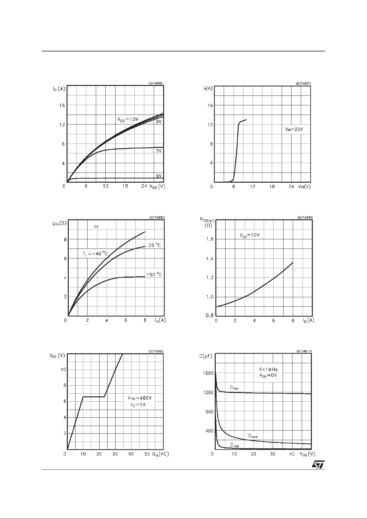
OutputCharacteristics
Transconductance
TransferCharacteristics
StaticDrain-sourceOn Resistance
GateCharge vs Gate-sourceVoltage
4/8
CapacitanceVariations
Page 5

STB7NB60
Normalized Gate Threshold Voltage vs
Temperature
Source-drainDiode Forward Characteristics
Normalized On Resistancevs Temperature
5/8
Page 6

STB7NB60
Fig. 1: Unclamped InductiveLoad TestCircuit
Fig. 3: SwitchingTimesTest CircuitsFor
ResistiveLoad
Fig. 2: Unclamped InductiveWaveform
Fig. 4: Gate Charge test Circuit
Fig. 5: Test Circuit For InductiveLoad Switching
And Diode RecoveryTimes
6/8
Page 7

TO-262(I2PAK) MECHANICALDATA
STB7NB60
DIM.
MIN. TYP. MAX. MIN. TYP. MAX.
A 4.3 4.6 0.169 0.181
A1 2.49 2.69 0.098 0.106
B 0.7 0.93 0.027 0.036
B1 1.2 1.38 0.047 0.054
B2 1.25 1.4 0.049 0.055
C 0.45 0.6 0.017 0.023
C2 1.21 1.36 0.047 0.053
D 8.95 9.35 0.352 0.368
e 2.44 2.64 0.096 0.104
E 10 10.28 0.393 0.404
L 13.2 13.5 0.519 0.531
L1 3.48 3.78 0.137 0.149
L2 1.27 1.4 0.050 0.055
mm inch
CA1
A
C2
B2
B
e
E
L1
L2
D
L
P011P5/C
7/8
Page 8

STB7NB60
TO-263(D2PAK) MECHANICAL DATA
DIM.
MIN. TYP. MAX. MIN. TYP. MAX.
A 4.3 4.6 0.169 0.181
A1 2.49 2.69 0.098 0.106
B 0.7 0.93 0.027 0.036
B2 1.25 1.4 0.049 0.055
C 0.45 0.6 0.017 0.023
C2 1.21 1.36 0.047 0.053
D 8.95 9.35 0.352 0.368
E 10 10.28 0.393 0.404
G 4.88 5.28 0.192 0.208
L 15 15.85 0.590 0.624
L2 1.27 1.4 0.050 0.055
L3 1.4 1.75 0.055 0.068
mm inch
E
A
C2
8/8
L2
D
L
L3
B2
B
A1
C
G
P011P6/C
Page 9

STB7NB60
Information furnished is believed tobe accurate and reliable. However, STMicroelectronicsassumes no responsibility for the consequences
of use of such information nor for any infringement of patents or other rights of third parties which may result from its use. No license is
granted by implication orotherwise under any patent or patent rights of STMicroelectronics. Specification mentioned in this publication are
subject tochange without notice. This publication supersedes and replaces all information previously supplied.STMicroelectronics products
are not authorized for use as critical componentsin life support devices or systems without express written approval of STMicroelectronics.
Australia - Brazil - Canada- China - France- Germany- Italy - Japan - Korea- Malaysia - Malta - Mexico- Morocco- The Netherlands-
Singapore- Spain- Sweden- Switzerland- Taiwan - Thailand -United Kingdom- U.S.A.
The ST logo isa trademarkof STMicroelectronics
1998 STMicroelectronics– Printedin Italy– All Rights Reserved
STMicroelectronicsGROUP OFCOMPANIES
.
9/8
 Loading...