

Page 1

STA309B
Multichannel digital audio processor with FFX
Features
■ 8 channels of 24-bit FFX
■
>100 dB SNR and dynamic range
■ Selectable 32 kH-192 kHz input sampling rates
■ 6 channels of DSD/SACD and PDM input
■ Digital gain/attenuation +58 dB to -100 dB in
0.5 dB steps
■ Advanced “pop-free” operation
■ Digital “pop-free” operation for single-ended
mode
■ Soft volume update
■ Individual channel and master gain/attenuation
plus channel trim (-10 dB to +10 dB)
■ Up to 10 independent 32-bit user-
programmable biquads (EQ) per channel
■ Bass/treble tone control
■ Pre- and post-EQ full 8-channel input mix on all
8 channels
■ Dual independent limiters/compressors
■ Dynamic range compression or anti-clipping
modes
■ AutoModes
– 5-band graphic EQ
– 32 preset EQ curves (rock, jazz, pop, etc.)
– Automatic volume controlled loudness
– 5.1 to 2-channel downmix
– Simultaneous 5.1- and 2-channel downmix
outputs
– 3 preset volume curves
– 2 preset anti-clipping modes
– Preset movie nighttime listening mode
– Preset TV channel/commercial AGC mode
– 5.1, 2.1 bass management configurations
– AM frequency automatic output PWM
frequency shifting
– 8 preset crossover filters
■ Individual channel and master soft/hard mute
®
®
Preliminary data
VFQFPN-56
■ Automatic zero-detect and invalid input mute
■ Automatic amplifier power-down on clock loss
■ Advanced AM interference frequency
switching and noise suppression modes
2
■ I
S output channel mapping function
■ Independent channel volume and DSP bypass
■ Channel mapping of any input to any
processing/FFX channel
■ Selectable per-channel FFX damped ternary or
binary PWM output
■ Max power correction for lower full-power THD
■ Variable per-channel FFX o
■ 192 kHz internal processing sampling rate,
utput delay control
24-bit to 36-bit precision
Description
The STA309B is a single-chip solution for digital
audio processing and control in multichannel
applications and provides output capabilities for
FFX (full flexible amplification). In conjunction with
an FFX power device, it provides high-quality,
high-efficiency, all-digital amplification. The device
is extremely versatile, allowing for input of most
digital formats including 6.1/7.1-channel and
192 kHz, 24-bit DVD-audio, DSD/SACD and PDM
for MEMS microphone inputs. In the 5.1
application, the additional 2 channels can be used
for audio line-out or headphone drive. In speaker
mode, with 8 channel outputs in parallel, the
STA309B can deliver 1 W (maximum).
Table 1. Device summary
Order code Package Packaging
STA309B VFQFPN56 Tube
STA309BTR VFQFPN56 Tape and reel
January 2012 Doc ID 022570 Rev 2 1/66
www.st.com
66
Page 2

Contents STA309B
Contents
1 Block diagram . . . . . . . . . . . . . . . . . . . . . . . . . . . . . . . . . . . . . . . . . . . . . . 8
2 Pin connections . . . . . . . . . . . . . . . . . . . . . . . . . . . . . . . . . . . . . . . . . . . . . 9
3 Electrical specifications . . . . . . . . . . . . . . . . . . . . . . . . . . . . . . . . . . . . . 12
3.1 Absolute maximum ratings . . . . . . . . . . . . . . . . . . . . . . . . . . . . . . . . . . . . 12
3.2 Thermal data . . . . . . . . . . . . . . . . . . . . . . . . . . . . . . . . . . . . . . . . . . . . . . 12
3.3 Recommended operating conditions . . . . . . . . . . . . . . . . . . . . . . . . . . . . 12
3.4 Electrical specifications . . . . . . . . . . . . . . . . . . . . . . . . . . . . . . . . . . . . . . 13
4 Pin description . . . . . . . . . . . . . . . . . . . . . . . . . . . . . . . . . . . . . . . . . . . . 14
5I
2
C bus operation . . . . . . . . . . . . . . . . . . . . . . . . . . . . . . . . . . . . . . . . . . 15
5.1 Communication protocol . . . . . . . . . . . . . . . . . . . . . . . . . . . . . . . . . . . . . . 15
5.1.1 Data transition or change . . . . . . . . . . . . . . . . . . . . . . . . . . . . . . . . . . . . 15
5.1.2 Start condition . . . . . . . . . . . . . . . . . . . . . . . . . . . . . . . . . . . . . . . . . . . . 15
5.1.3 Stop condition . . . . . . . . . . . . . . . . . . . . . . . . . . . . . . . . . . . . . . . . . . . . 15
5.1.4 Data input . . . . . . . . . . . . . . . . . . . . . . . . . . . . . . . . . . . . . . . . . . . . . . . 15
5.2 Device addressing . . . . . . . . . . . . . . . . . . . . . . . . . . . . . . . . . . . . . . . . . . 15
5.3 Write operation . . . . . . . . . . . . . . . . . . . . . . . . . . . . . . . . . . . . . . . . . . . . . 16
5.3.1 Byte write . . . . . . . . . . . . . . . . . . . . . . . . . . . . . . . . . . . . . . . . . . . . . . . . 16
5.3.2 Multi-byte write . . . . . . . . . . . . . . . . . . . . . . . . . . . . . . . . . . . . . . . . . . . . 16
6 Application reference schematic . . . . . . . . . . . . . . . . . . . . . . . . . . . . . . 17
7 Registers . . . . . . . . . . . . . . . . . . . . . . . . . . . . . . . . . . . . . . . . . . . . . . . . . 18
7.1 Register summary . . . . . . . . . . . . . . . . . . . . . . . . . . . . . . . . . . . . . . . . . . 18
7.2 Register description . . . . . . . . . . . . . . . . . . . . . . . . . . . . . . . . . . . . . . . . . 22
7.2.1 Configuration register A (0x00) . . . . . . . . . . . . . . . . . . . . . . . . . . . . . . . 22
7.2.2 Configuration register B (0x01) - serial input formats . . . . . . . . . . . . . . 24
7.2.3 Configuration register C (0x02) - serial output formats . . . . . . . . . . . . . 26
7.2.4 Configuration register D (0x03) . . . . . . . . . . . . . . . . . . . . . . . . . . . . . . . 27
7.2.5 Configuration register E (0x04) . . . . . . . . . . . . . . . . . . . . . . . . . . . . . . . 28
7.2.6 Configuration register F (0x05) . . . . . . . . . . . . . . . . . . . . . . . . . . . . . . . 28
2/66 Doc ID 022570 Rev 2
Page 3

STA309B Contents
7.2.7 Configuration register G (0x06) . . . . . . . . . . . . . . . . . . . . . . . . . . . . . . . 30
7.2.8 Configuration register H (0x07) . . . . . . . . . . . . . . . . . . . . . . . . . . . . . . . 31
7.2.9 Configuration register I (0x08) . . . . . . . . . . . . . . . . . . . . . . . . . . . . . . . . 32
7.2.10 Master mute register (0x09) . . . . . . . . . . . . . . . . . . . . . . . . . . . . . . . . . . 33
7.2.11 Master volume register (0x0A) . . . . . . . . . . . . . . . . . . . . . . . . . . . . . . . . 33
7.2.12 Channel 1 volume (0x0B) . . . . . . . . . . . . . . . . . . . . . . . . . . . . . . . . . . . 33
7.2.13 Channel 2 volume (0x0C) . . . . . . . . . . . . . . . . . . . . . . . . . . . . . . . . . . . 33
7.2.14 Channel 3 volume (0x0D) . . . . . . . . . . . . . . . . . . . . . . . . . . . . . . . . . . . 33
7.2.15 Channel 4 volume (0x0E) . . . . . . . . . . . . . . . . . . . . . . . . . . . . . . . . . . . 33
7.2.16 Channel 5 volume (0x0F) . . . . . . . . . . . . . . . . . . . . . . . . . . . . . . . . . . . . 34
7.2.17 Channel 6 volume (0x10) . . . . . . . . . . . . . . . . . . . . . . . . . . . . . . . . . . . . 34
7.2.18 Channel 7 volume (0x11) . . . . . . . . . . . . . . . . . . . . . . . . . . . . . . . . . . . . 34
7.2.19 Channel 8 volume (0x12) . . . . . . . . . . . . . . . . . . . . . . . . . . . . . . . . . . . . 34
7.2.20 Channel 1 volume trim, mute, bypass (0x13) . . . . . . . . . . . . . . . . . . . . 34
7.2.21 Channel 2 volume trim, mute, bypass (0x14) . . . . . . . . . . . . . . . . . . . . 34
7.2.22 Channel 3 volume trim, mute, bypass (0x15) . . . . . . . . . . . . . . . . . . . . 34
7.2.23 Channel 4 volume trim, mute, bypass (0x16) . . . . . . . . . . . . . . . . . . . . 35
7.2.24 Channel 5 volume trim, mute, bypass (0x17) . . . . . . . . . . . . . . . . . . . . 35
7.2.25 Channel 6 volume trim, mute, bypass (0x18) . . . . . . . . . . . . . . . . . . . . 35
7.2.26 Channel 7 volume trim, mute, bypass (0x19) . . . . . . . . . . . . . . . . . . . . 35
7.2.27 Channel 8 volume trim, mute, bypass (0x1A) . . . . . . . . . . . . . . . . . . . . 35
7.2.28 Channel input mapping channels 1 and 2 (0x1B) . . . . . . . . . . . . . . . . . 37
7.2.29 Channel input mapping channels 3 and 4 (0x1C) . . . . . . . . . . . . . . . . . 37
7.2.30 Channel input mapping channels 5 and 6 (0x1D) . . . . . . . . . . . . . . . . . 37
7.2.31 Channel input mapping channels 7 and 8 (0x1E) . . . . . . . . . . . . . . . . . 37
7.2.32 AUTO1 - AutoModes EQ, volume, GC (0x1F) . . . . . . . . . . . . . . . . . . . . 38
7.2.33 AUTO2 - AutoModes bass management2 (0x20) . . . . . . . . . . . . . . . . . 39
7.2.34 AUTO3 - AutoMode AM/pre-scale/bass management scale (0x21) . . . 40
7.2.35 PREEQ - preset EQ settings (0x22) . . . . . . . . . . . . . . . . . . . . . . . . . . . 41
7.2.36 AGEQ - graphic EQ 80-Hz band (0x23) . . . . . . . . . . . . . . . . . . . . . . . . . 42
7.2.37 BGEQ - graphic EQ 300-Hz band (0x24) . . . . . . . . . . . . . . . . . . . . . . . . 42
7.2.38 CGEQ - graphic EQ 1-kHz band (0x25) . . . . . . . . . . . . . . . . . . . . . . . . . 42
7.2.39 DGEQ - graphic EQ 3-kHz band (0x26) . . . . . . . . . . . . . . . . . . . . . . . . . 42
7.2.40 EGEQ - graphic EQ 8-kHz band (0x27) . . . . . . . . . . . . . . . . . . . . . . . . . 43
7.2.41 Biquad internal channel loop-through (0x28) . . . . . . . . . . . . . . . . . . . . . 43
7.2.42 Mix internal channel loop-through (0x29) . . . . . . . . . . . . . . . . . . . . . . . 44
7.2.43 EQ bypass (0x2A) . . . . . . . . . . . . . . . . . . . . . . . . . . . . . . . . . . . . . . . . . 44
Doc ID 022570 Rev 2 3/66
Page 4

Contents STA309B
7.2.44 Tone control bypass (0x2B) . . . . . . . . . . . . . . . . . . . . . . . . . . . . . . . . . . 44
7.2.45 Tone control (0x2C) . . . . . . . . . . . . . . . . . . . . . . . . . . . . . . . . . . . . . . . . 45
7.2.46 Channel limiter select channels 1,2,3,4 (0x2D) . . . . . . . . . . . . . . . . . . . 45
7.2.47 Channel limiter select channels 5,6,7,8 (0x2E) . . . . . . . . . . . . . . . . . . . 45
7.2.48 Limiter 1 attack/release rate (0x2F) . . . . . . . . . . . . . . . . . . . . . . . . . . . . 45
7.2.49 Limiter 1 attack/release threshold (0x30) . . . . . . . . . . . . . . . . . . . . . . . . 46
7.2.50 Limiter 2 attack/release rate (0x31) . . . . . . . . . . . . . . . . . . . . . . . . . . . . 46
7.2.51 Limiter 2 attack/release threshold (0x32) . . . . . . . . . . . . . . . . . . . . . . . . 46
7.2.52 Bit description . . . . . . . . . . . . . . . . . . . . . . . . . . . . . . . . . . . . . . . . . . . . 46
7.2.53 Channel 1 and 2 output timing (0x33) . . . . . . . . . . . . . . . . . . . . . . . . . . 50
7.2.54 Channel 3 and 4 output timing (0x34) . . . . . . . . . . . . . . . . . . . . . . . . . . 50
7.2.55 Channel 5 and 6 output timing (0x35) . . . . . . . . . . . . . . . . . . . . . . . . . . 50
7.2.56 Channel 7 and 8 output timing (0x36) . . . . . . . . . . . . . . . . . . . . . . . . . . 51
7.2.57 Channel I
7.2.58 Channel I
7.2.59 Channel I
7.2.60 Channel I
2
S output mapping channels 1 and 2 (0x37) . . . . . . . . . . . . . 51
2
S output mapping channels 3 and 4 (0x38) . . . . . . . . . . . . . 51
2
S output mapping channels 5 and 6 (0x39) . . . . . . . . . . . . . 51
2
S output mapping channels 7 and 8 (0x3A) . . . . . . . . . . . . . 52
7.2.61 Coefficient address register 1 (0x3B) . . . . . . . . . . . . . . . . . . . . . . . . . . 52
7.2.62 Coefficient address register 2 (0x3C) . . . . . . . . . . . . . . . . . . . . . . . . . . 52
7.2.63 Coefficient b1 data register, bits 23:16 (0x3D) . . . . . . . . . . . . . . . . . . . . 52
7.2.64 Coefficient b1 data register, bits 15:8 (0x3E) . . . . . . . . . . . . . . . . . . . . . 53
7.2.65 Coefficient b1 data register, bits 7:0 (0x3F) . . . . . . . . . . . . . . . . . . . . . . 53
7.2.66 Coefficient b2 data register, bits 23:16 (0x40) . . . . . . . . . . . . . . . . . . . . 53
7.2.67 Coefficient b2 data register, bits 15:8 (0x41) . . . . . . . . . . . . . . . . . . . . . 53
7.2.68 Coefficient b2 data register, bits 7:0 (0x42) . . . . . . . . . . . . . . . . . . . . . . 53
7.2.69 Coefficient a1 data register, bits 23:16 (0x43) . . . . . . . . . . . . . . . . . . . . 53
7.2.70 Coefficient a1 data register, bits 15:8 (0x44) . . . . . . . . . . . . . . . . . . . . . 53
7.2.71 Coefficient a1 data register, bits 7:0 (0x45) . . . . . . . . . . . . . . . . . . . . . . 54
7.2.72 Coefficient a2 data register, bits 23:16 (0x46) . . . . . . . . . . . . . . . . . . . . 54
7.2.73 Coefficient a2 data register, bits 15:8 (0x47) . . . . . . . . . . . . . . . . . . . . . 54
7.2.74 Coefficient a2 data register, bits 7:0 (0x48) . . . . . . . . . . . . . . . . . . . . . . 54
7.2.75 Coefficient b0 data register, bits 23:16 (0x49) . . . . . . . . . . . . . . . . . . . . 54
7.2.76 Coefficient b0 data register, bits 15:8 (0x4A) . . . . . . . . . . . . . . . . . . . . . 54
7.2.77 Coefficient b0 data register, bits 7:0 (0x4B) . . . . . . . . . . . . . . . . . . . . . . 54
7.2.78 Coefficient write control register (0x4C) . . . . . . . . . . . . . . . . . . . . . . . . . 55
7.3 Reading a coefficient from RAM . . . . . . . . . . . . . . . . . . . . . . . . . . . . . . . . 55
7.4 Reading a set of coefficients from RAM . . . . . . . . . . . . . . . . . . . . . . . . . . 55
4/66 Doc ID 022570 Rev 2
Page 5

STA309B Contents
7.5 Writing a single coefficient to RAM . . . . . . . . . . . . . . . . . . . . . . . . . . . . . 56
7.6 Writing a set of coefficients to RAM . . . . . . . . . . . . . . . . . . . . . . . . . . . . . 56
8 Equalization and mixing . . . . . . . . . . . . . . . . . . . . . . . . . . . . . . . . . . . . . 57
8.1 Post-scale . . . . . . . . . . . . . . . . . . . . . . . . . . . . . . . . . . . . . . . . . . . . . . . . . 57
8.2 Variable maximum power correction . . . . . . . . . . . . . . . . . . . . . . . . . . . . 59
8.2.1 MPCC1-2 (0x4D, 0x4E) . . . . . . . . . . . . . . . . . . . . . . . . . . . . . . . . . . . . . 59
8.3 Variable distortion compensation . . . . . . . . . . . . . . . . . . . . . . . . . . . . . . . 59
8.3.1 DCC1-2 (0x4F, 0x50) . . . . . . . . . . . . . . . . . . . . . . . . . . . . . . . . . . . . . . . 59
8.4 PSCorrect registers . . . . . . . . . . . . . . . . . . . . . . . . . . . . . . . . . . . . . . . . . 60
8.4.1 PSC1-2: ripple correction value (RCV) (0x51, 0x52) . . . . . . . . . . . . . . . 60
8.4.2 PSC3: correction normalization value (CNV) (0x53) . . . . . . . . . . . . . . . 60
8.5 Digital pop-free operation in single-ended mode . . . . . . . . . . . . . . . . . . . 60
8.5.1 PFCXON: digital pop-free register (0x5F) . . . . . . . . . . . . . . . . . . . . . . . 61
8.5.2 Timing settings . . . . . . . . . . . . . . . . . . . . . . . . . . . . . . . . . . . . . . . . . . . . 61
8.5.3 RAMPTIM: ramp duration register (0x66) . . . . . . . . . . . . . . . . . . . . . . . 62
8.5.4 TSPUPT: waiting time after EAPD (0x67 - 0x68) . . . . . . . . . . . . . . . . . . 62
8.5.5 LSPDWT: waiting time before EAPD (0x71 - 0x72) . . . . . . . . . . . . . . . . 62
9 Package information . . . . . . . . . . . . . . . . . . . . . . . . . . . . . . . . . . . . . . . . 63
10 Revision history . . . . . . . . . . . . . . . . . . . . . . . . . . . . . . . . . . . . . . . . . . . 65
Doc ID 022570 Rev 2 5/66
Page 6

List of tables STA309B
List of tables
Table 1. Device summary . . . . . . . . . . . . . . . . . . . . . . . . . . . . . . . . . . . . . . . . . . . . . . . . . . . . . . . . . . 1
Table 2. Pin description . . . . . . . . . . . . . . . . . . . . . . . . . . . . . . . . . . . . . . . . . . . . . . . . . . . . . . . . . . 10
Table 3. Absolute maximum ratings . . . . . . . . . . . . . . . . . . . . . . . . . . . . . . . . . . . . . . . . . . . . . . . . . 12
Table 4. Thermal data. . . . . . . . . . . . . . . . . . . . . . . . . . . . . . . . . . . . . . . . . . . . . . . . . . . . . . . . . . . . 12
Table 5. Recommended operating conditions . . . . . . . . . . . . . . . . . . . . . . . . . . . . . . . . . . . . . . . . . 12
Table 6. General interface electrical specifications . . . . . . . . . . . . . . . . . . . . . . . . . . . . . . . . . . . . . 13
Table 7. DC electrical characteristics: 3.3-V buffers . . . . . . . . . . . . . . . . . . . . . . . . . . . . . . . . . . . . . 13
Table 8. Register summary. . . . . . . . . . . . . . . . . . . . . . . . . . . . . . . . . . . . . . . . . . . . . . . . . . . . . . . . 18
Table 9. RAM block for biquads, mixing, and bass management. . . . . . . . . . . . . . . . . . . . . . . . . . . 57
Table 10. VFQFPN-56 (8 x 8 mm) package dimensions . . . . . . . . . . . . . . . . . . . . . . . . . . . . . . . . . . 63
Table 11. Exposed pad variations . . . . . . . . . . . . . . . . . . . . . . . . . . . . . . . . . . . . . . . . . . . . . . . . . . . 63
Table 12. Document revision history . . . . . . . . . . . . . . . . . . . . . . . . . . . . . . . . . . . . . . . . . . . . . . . . . 65
6/66 Doc ID 022570 Rev 2
Page 7

STA309B List of figures
List of figures
Figure 1. Block diagram . . . . . . . . . . . . . . . . . . . . . . . . . . . . . . . . . . . . . . . . . . . . . . . . . . . . . . . . . . . 8
Figure 2. Channel signal flow . . . . . . . . . . . . . . . . . . . . . . . . . . . . . . . . . . . . . . . . . . . . . . . . . . . . . . . 8
Figure 3. Pin connections (top view) . . . . . . . . . . . . . . . . . . . . . . . . . . . . . . . . . . . . . . . . . . . . . . . . . . 9
Figure 4. Write mode sequence . . . . . . . . . . . . . . . . . . . . . . . . . . . . . . . . . . . . . . . . . . . . . . . . . . . . 16
Figure 5. Read mode sequence . . . . . . . . . . . . . . . . . . . . . . . . . . . . . . . . . . . . . . . . . . . . . . . . . . . . 16
Figure 6. Reference schematic for STA309B-based application . . . . . . . . . . . . . . . . . . . . . . . . . . . 17
Figure 7. Basic limiter and volume flow diagram . . . . . . . . . . . . . . . . . . . . . . . . . . . . . . . . . . . . . . . 47
Figure 8. Channel mixer . . . . . . . . . . . . . . . . . . . . . . . . . . . . . . . . . . . . . . . . . . . . . . . . . . . . . . . . . . 57
Figure 9. Typical single-ended driver - power stage configuration. . . . . . . . . . . . . . . . . . . . . . . . . . . 61
Figure 10. Pop-free timing diagram . . . . . . . . . . . . . . . . . . . . . . . . . . . . . . . . . . . . . . . . . . . . . . . . . . . 61
Figure 11. VFQFPN-56 (8 x 8 mm) package outline . . . . . . . . . . . . . . . . . . . . . . . . . . . . . . . . . . . . . . 64
Doc ID 022570 Rev 2 7/66
Page 8

Block diagram STA309B
1 Block diagram
Figure 1. Block diagram
SA
SCL
LRCKI
BICKI
SDI12
SDI34
SDI56
SERIAL
DATA
IN
SYSTEM
CONTROL
SDI78
CHANNEL
MAPPING
VARIABLE
OVER-
SAMPLING
SYSTEM TIMING
PLLB
PLL
XTI
CKOUT
Figure 2. Channel signal flow
6 Inputs
From DSD
DSD
Conversion
SDA
I2C
PWDN
POWER
DOWN
MVO
OVERSAMPLING
TREBLE,
BASS, EQ
(BIQUADS )
EAPD
VOLUME
LIMITING
VARIABLE
DOWN-
SAMPLING
DDX
FFX
SERIAL
DATA
OUT
OUT1A/B
OUT2A/B
OUT3A/B
OUT4A/B
OUT5A/B
OUT6A/B
OUT7A/B
OUT8A/B
LRCKO
BICKO
SDO12
SDO34
SDO56
SDO78
Interp_Rate
8 Inputs
From I2S
From
Mix#1
Engine
Or
Previous
Channel
Biq u a d # 1 0
Output
(CxBLP)
PreScale
Hard Set to
-18dB when
Aut oMod e EQ
(AMEQ)
1x,2x,4x
Interp
Distortion
Compensation
High - P a s s
Filt er
Use r Pr og amm ab le
Biqu ad #1 wh en
High-Pass Bypassed
(HPB)
Biq u a d
DSDE
Mapp ing/
Mix #1
Biq u ad s
B/ T
NS C_Con PWM
Biqu ad
#2
Biqu ad
#3
Hard Set Coeec ients wh en AutoMode EQ
(AMEQ)
Biqu a d
#4
#5
8/66 Doc ID 022570 Rev 2
Biquad
#6
Mix #2
Coeecients when
Bass Management
Biquad
#7
Hard Se t
Aut o Mo d e
Cross over
(AMBMXE)
Vol um e
Limiter
Biqu a d
#8
Hard Se t
Coeecient s when
DeEmphasis
Enab led
(DEMP)
2x
Interp
DDX
Output
Bas s
Use r Pr og ram mab le
Biquads #9 and #10
When Tone Bypass ed
(CxTCB)
Treble
To
Mix# 2
Engine
Page 9

STA309B Pin connections
2 Pin connections
Figure 3. Pin connections (top view)
PWDN
SDO_78
SDO_56
GND
VDD
SDO_34
SDO_12
LRCKO
BICKO
GND
VDD EAPD
56
1 MVO
2 GND
3 VDD
4 GND
5 SDI_78
6 SDI_56
7 SDI_34
8 SDI_12
9 LRCKI
10 BICKI
11 VDD
12 GND
55
54
52
51
53
VFQFPN-56
50
49
48
47
46
45
OUT1_A
44
OUT1_B
43
42
41
40
39
38
37
36
35
34
33
32
31
OUT2_A
OUT2B
GND
VDD
OUT3_A
OUT3_B
OUT4_A
OUT4_B
OUT5_A
OUT5_B
GND
VDD
13 RESET
14 BYPASS
15
SA
16 SDA
SCL
17
XTI 19 FILTER_PLL
18
20
GNDA
22 CKOUT
21 VDDA
23 GND
25 OUT8_B
24 VDD
26 OUT8_A
27
OUT7_B
28
OUT7_A
30
29
OUT6_A
OUT6_B
Doc ID 022570 Rev 2 9/66
Page 10

Pin connections STA309B
Table 2. Pin description
STA309B pin Type Name Description
1 5-V tolerant TTL input buffer MVO/DSD_CLK
5 5-V tolerant TTL input buffer SDI_78/DSD_6
6 5-V tolerant TTL input buffer SDI_56/DSD_5
7 5-V tolerant TTL input buffer SDI_34/DSD_4
8 5-V tolerant TTL input buffer SDI_12/DSD_3
9 5-V tolerant TTL input buffer LRCKI/DSD_2
10 5-V tolerant TTL input buffer BICKI/DSD_1
13
5-V tolerant TTL schmitt trigger
input buffer
RESET Global reset
Master volume override/
DSD input clock
Input serial data channels 7 & 8/
DSD input channel 6
Input serial data channels 5 & 6/
DSD input channel 5
Input serial data channels 3 & 4/
DSD input channel 4
Input serial data channels 1 & 2/
DSD input channel 3
Input left/right clock/
DSD input channel 2
Input serial clock/
DSD input channel 1
14 CMOS input buffer with pull-down PLL_BYPASS Bypass phase locked loop
15 CMOS input buffer with pull-down SA Select address (I
16
Bidirectional buffer: 5-V tolerant TTL
schmitt trigger input; 3.3-V capable
SDA Serial data (I
2
C)
2 mA slew-rate controlled output
17
18
5-V tolerant TTL schmitt trigger
input buffer
5-V tolerant TTL schmitt trigger
input buffer
SCL Serial clock (I
XTI Crystal oscillator input (clock input)
2
C)
2
C)
19 Analog pad FILTER_PLL PLL filter
20 Analog ground GNDA PLL ground
21 3.3V analog supply voltage VDDA PLL supply
22
25
26
27
28
29
3.3-V capable TTL tristate 4mA
output buffer
3.3-V capable TTL 2mA output
buffer
3.3-V capable TTL 2mA output
buffer
3.3-V capable TTL 2mA output
buffer
3.3-V capable TTL 2mA output
buffer
3.3-V capable TTL 2mA output
buffer
CKOUT Clock output
OUT8B PWM channel 8 output B
OUT8A PWM channel 8 output A
OUT7B PWM channel 7 output B
OUT7A PWM channel 7 output A
OUT6B PWM channel 6 output B
10/66 Doc ID 022570 Rev 2
Page 11

STA309B Pin connections
Table 2. Pin description (continued)
STA309B pin Type Name Description
30
33
34
35
36
37
38
41
42
43
44
45
3.3-V capable TTL 2mA output
buffer
3.3-V capable TTL 2mA output
buffer
3.3-V capable TTL 2mA output
buffer
3.3-V capable TTL 2mA output
buffer
3.3-V capable TTL 2mA output
buffer
3.3-V capable TTL 2mA output
buffer
3.3-V capable TTL 2mA output
buffer
3.3-V capable TTL 2mA output
buffer
3.3-V capable TTL 2mA output
buffer
3.3-V capable TTL 2mA output
buffer
3.3-V capable TTL 2mA output
buffer
3.3-V capable TTL 4mA output
buffer
OUT6A PWM channel 6 output A
OUT5B PWM channel 5 output B
OUT5A PWM channel 5 output A
OUT4B PWM channel 4 output B
OUT4A PWM channel 4 output A
OUT3B PWM channel 3 output B
OUT3A PWM channel 3 output A
OUT2B PWM channel 2 output B
OUT2A PWM channel 2 output A
OUT1B PWM channel 1 output B
OUT1A PWM channel 1 output A
EAPD Ext. amp power-down
48
49
50
51
54
55
56
3,11,21,24,31,39,
46,52
2,4,12,20,23,32,
40,47,53
3.3-V capable TTL 2mA output
buffer
3.3-V capable TTL 2mA output
buffer
3.3-V capable TTL 2mA output
buffer
3.3-V capable TTL 2mA output
buffer
3.3-V capable TTL 2mA output
buffer
3.3-V capable TTL 2mA output
buffer
5-V tolerant TTL schmitt trigger
input buffer
3.3-V digital supply voltage VDD 3.3-V supply
Digital ground GND Ground
Doc ID 022570 Rev 2 11/66
BICKO Output serial clock
LRCKO Output left/right clock
SDO_12 Output serial data channels 1&2
SDO_34 Output serial data channels 3&4
SDO_56 Output serial data channels 5&6
SDO_78 Output serial data channels 7&8
PWDN Device power-down
Page 12

Electrical specifications STA309B
3 Electrical specifications
3.1 Absolute maximum ratings
Table 3. Absolute maximum ratings
Symbol Parameter Min Typ Max Unit
V
V
V
V
T
T
DD
DDA
i
o
stg
amb
3.3-V I/O power supply -0.5 4 V
3.3-V logic power supply -0.5 4 V
Voltage on input pins -0.5 VDD + 0.5 V
Voltage on output pins -0.5 VDD + 0.3 V
Storage temperature -40 150 °C
Ambient operating temperature -40 90 °C
3.2 Thermal data
Table 4. Thermal data
Symbol Parameter Min Typ Max Unit
R
thj-case
Thermal resistance, junction-case (thermal pad)
STA309B
3.3 Recommended operating conditions
Table 5. Recommended operating conditions
Symbol Parameter Min Typ Max Unit
1.5 °C/W
V
V
T
DD
DDA
j
I/O power supply 3.0 3.6 V
Logic power supply 3.0 3.6 V
Operating junction temperature -40 125 °C
12/66 Doc ID 022570 Rev 2
Page 13

STA309B Electrical specifications
3.4 Electrical specifications
The following specifications are valid for VDD = 3.3 V ± 0.3 V, V
= 3.3 V ± 0.3 V and
DDA
Tamb = 0 to 70 °C, unless otherwise stated.
Table 6. General interface electrical specifications
Symbol Parameter Conditions Min Typ Max Unit
I
il
I
ih
I
OZ
V
esd
1. The leakage currents are generally very small, < 1 nA. The values given here are maximum after an
electrostatic stress on the pin.
Table 7. DC electrical characteristics: 3.3-V buffers
Low-level input no pull-up Vi = 0 V 1
High-level input no
pull-down
Tristate output leakage
without pull-up/down
Electrostatic protection
(human body model)
V
= VDD 2μA
i
= VDD 2μA
V
i
Leakage < 1μA2000V
Symbol Parameter Conditions Min Typ Max Unit
V
IL
V
IH
V
ILhyst
V
IHhyst
V
hyst
V
ol
V
oh
Low-level input voltage 0.8 V
High-level input voltage 2.0 V
Low-level threshold Input falling 0.8 1.35 V
High-level threshold Input rising 1.3 2.0 V
Schmitt trigger hysteresis 0.3 0.8 V
Low-level output IoI = 100 µA 0.2 V
High-level output
Ioh = -100 µA
VDD-
0.2
Ioh = -2 mA 2.4 V
(1)
μA
V
Doc ID 022570 Rev 2 13/66
Page 14

Pin description STA309B
4 Pin description
Master volume override (MVO)
This pin enables the user to bypass the volume control on all channels. When MVO is pulled
high, the master volume register is set to 0x00, which corresponds to its full-scale setting.
The master volume register setting offsets the individual channel volume settings, which
default to 0 dB.
Serial data in (SDI_12, SDI_34, SDI_56, SDI_78)
Audio information enters the device here. Six format choices are available including I2S,
left- or right-justified, LSB or MSB first, with word widths of 16, 18, 20 and 24 bits.
RESET
Driving this pin low turns off the outputs and returns all settings to their defaults.
I2C bus
The SA, SDA and SCL pins operate per the Phillips I2C specification. See Section 5: I2C
bus operation.
Phase locked loop (PLL)
The phase locked loop section provides the system timing signals and CKOUT.
Clock output (CKOUT)
System synchronization and master clocks are provided by CKOUT.
PWM outputs (OUT1 through OUT8)
The PWM outputs provide the input signal for the power devices.
External amplifier power-down (EAPD)
This signal can be used to control the power-down of FFX power devices.
Serial data out (SDO_12, SDO_34, SDO_56, SDO_78)
These are the outputs for audio information. Six different formats are available including I2S,
left- or right-justified, LSB or MSB first, with word widths of 16, 18, 20 and 24 bits.
Device power-down (PWDN)
Pulling PWDN low begins the power-down sequence which puts the STA309B into a
low-power state. EAPD (pin 51) goes low approximately 30 ms later.
14/66 Doc ID 022570 Rev 2
Page 15

STA309B I2C bus operation
5 I2C bus operation
The STA309B supports the I2C protocol via the input ports SCL and SDA_IN (master to
slave) and the output port SDA_OUT (slave to master).
This protocol defines any device that sends data on to the bus as a transmitter and any
device that reads the data as a receiver.
The device that controls the data transfer is known as the master and the other as the slave.
The master always starts the transfer and provides the serial clock for synchronization. The
STA309B is always a slave device in all of its communications.
5.1 Communication protocol
5.1.1 Data transition or change
Data changes on the SDA line must only occur when the SCL clock is low. An SDA transition
while the clock is high is used to identify a START or STOP condition.
5.1.2 Start condition
START is identified by a high to low transition of the data bus SDA signal while the clock
signal SCL is stable in the high state. A START condition must precede any command for
data transfer.
5.1.3 Stop condition
STOP is identified by low to high transition of the data bus SDA signal while the clock signal
SCL is stable in the high state. A STOP condition terminates communication between the
STA309B and the bus master.
5.1.4 Data input
During the data input the STA309B samples the SDA signal on the rising edge of clock SCL.
For correct device operation the SDA signal must be stable during the rising edge of the
clock and the data can change only when the SCL line is low.
5.2 Device addressing
To start communication between the master and the Omega FFX core, the master must
initiate with a start condition. Following this, the master sends 8 bits to the SDA line (MSB
first) corresponding to the device select address and read or write mode.
The 7 most significant bits are the device address identifiers, corresponding to the I
definition. In the STA309B the I
port configuration, 0x40 or 0100000x when SA = 0, and 0x42 or 0100001x when SA = 1.
th
The 8
for write mode. After a START condition, the STA309B identifies on the bus the device
address and if a match is found, it acknowledges the identification on the SDA bus during
bit (LSB) identifies read or write operation RW, this bit is set to 1 in read mode and 0
2
C interface has two device addresses depending on the SA
2
C bus
Doc ID 022570 Rev 2 15/66
Page 16

I2C bus operation STA309B
the 9th-bit time. The byte following the device identification byte is the internal space
address.
5.3 Write operation
Following the START condition the master sends a device select code with the RW bit set
to 0. The STA309B acknowledges this and then waits for the byte of internal address.
After receiving the internal byte address the STA309B again responds with an
acknowledgement.
5.3.1 Byte write
In the byte write mode the master sends one data byte, this is acknowledged by the FFX
core. The master then terminates the transfer by generating a STOP condition.
5.3.2 Multi-byte write
The multi-byte write modes can start from any internal address. The master generating a
STOP condition terminates the transfer.
Figure 4. Write mode sequence
BYTE
WRITE
DEV-ADDR
START RW
ACK
ACK
MULTIBYTE
WRITE
DEV-ADDR
START RW
Figure 5. Read mode sequence
ACK
CURRENT
ADDRESS
READ
RANDOM
ADDRESS
READ
SEQUENTIAL
CURRENT
READ
SEQUENTIAL
RANDOM
READ
START
START
START
START
DEV-ADDR
DEV-ADDR
DEV-ADDR
DEV-ADDR
RW=
HIGH
DATA
RW
ACK
SUB-ADDR
RW
ACK
DATA
ACK
SUB-ADDR
RW
SUB-ADDR
SUB-ADDR
NO ACK
ACK
ACK
ACK
STOP
DATA
DEV-ADDR
DEV-ADDR
ACK
ACK
CK
A
DATA IN
STOP
DATA IN
CK
DATA IN
ACK
A
STOP
CK
A
WRTRATS
ACK
CK
A
WRTRATS
DATA
DATA
DATA
NO ACK
NO A
CK
A
STOP
CK
STOP
DATA
CK NO ACK
A
DATA
STOP
16/66 Doc ID 022570 Rev 2
Page 17

STA309B Application reference schematic
6 Application reference schematic
Figure 6. Reference schematic for STA309B-based application
+3.3V
2.2UF
2.2UF
EIA3216_A
EIA3216_A
C4
6.3VDC
C4
6.3VDC
+
+
C12
C12
Y5V
100NF
100NF
EIA0603
Y5V
EIA0603
+3.3V
C20
100NF
Y5V
EIA0603
C20
100NF
Y5V
EIA0603
EAPD
2
L1
L1
EIA0805
EIA0805
R6
0
R6
0
0000-0603
0000-0603
+3.3V
C14
C14
Y5V
Y5V
100NF
100NF
EIA0603
EIA0603
1
600 ohm@100mhz
600 ohm@100mhz
2
L3
L3
EIA0805
EIA0805
1
600 ohm@100mhz
600 ohm@100mhz
+3.3V
+3.3V
C145
C145
C18
C18
100NF
100NF
100NF
100NF
Y5V
Y5V
Y5V
Y5V
EIA0603
EIA0603
EIA0603
EIA0603
CH1_A
C147 1000PF
C147 1000PF
PWRDWN
CH1_B
NPO
NPO
EIA0805
EIA0805
CH2_A
CH3_A
44
OUT3_A43OUT3_B
VDD3.3_5
SDI_78
5
6
CH3_B
42
41
SDI_56
8
7
SDATA2
CH4_A
CH4_B
OUT4_A
OUT4_B40OUT5_A
SDI_12
SDI_34
9
SDATA1
SDATA0
CH5_A
39
LRCKI
10
LRCK
38
11
CH2_B
45
47
46
48
U2
NC 46
GND_5
OUT2_A
OUT2_B
OUT1_B
49
OUT1_A
50
EAPD
51
VDD3.3_6
52
GND_6
53
NC 54
54
BICKO
55
LRCKO
56
SDO_12
57
SDO_34
58
VDD3.3_7
59
GND_7
60
NC 61
61
SDO_56
62
SDO_78
63
PWDN
64
VDD3.3_1
TEST_MODE
GND_14NC 5
MVO
3
2
1
0
0
0000-0603
0000-0603
R14
R14
CH5_B
37
NC 37
OUT5_B
VDD3.3_2
BICKI
12
BICK
36
GND_4
GND_2
13
35
14
CH6_B
CH6_A
34
33
OUT6_A
OUT6_B
VDD3.3_4
PLL_BYPASS
NC 14
RESET
16
15
STA308AU2STA308A
OUT7_A
32
OUT7_B
31
OUT8_A
30
OUT8_B
29
VDD3.3_3
28
GND_3
27
NC 26
26
CKOUT
25
VDD3.3_PLL
24
GNDA_PLL
23
VDDA_PLL
22
PLL_FILTER
21
XTI
20
SCL
19
SDA
18
SA
17
NPO
NPO
C157
C157
47PF
47PF
NPO
NPO
1000PF
1000PF
C155
C155
EIA0603
EIA0603
EIA0603
EIA0603
+3.3V
C25
C25
C23
C23
Y5V
Y5V
100NF
100NF
100NF
Y5V
100NF
Y5V
EIA0603
EIA0603
EIA0603
EIA0603
SDA
VDDA
SCL
MCLK
C22
C22
+
+
C24
C24
22UF
22UF
100NF
100NF
R15
R15
EIA3528_B
EIA3528_B
6.3VDC
6.3VDC
Y5V
Y5V
EIA0603
EIA0603
C19
C19
220PF
220PF
3.40K
3.40K
0603
0603
NPO
NPO
EIA0603
EIA0603
C16
C16
C15
C15
NPO
NPO
100PF
100PF
1200PF
1200PF
X7R
X7R
The PLL filter must be placed as close
GNDA
EIA0603
EIA0603
EIA0603
EIA0603
as possible to the STA309B pins
+3.3V
Y5V
Y5V
100NF
EIA0603
100NF
EIA0603
C5
C5
+3.3V
Y5V
Y5V
C6
100NF
C6
100NF
EIA0603
EIA0603
POWER_ON_RST
Doc ID 022570 Rev 2 17/66
Page 18

Registers STA309B
7 Registers
7.1 Register summary
Table 8. Register summary
Addr Name D7 D6 D5 D4 D3 D2 D1 D0
Configuration
0x00 CONFA COS1 COS0 DSPB IR1 IR0 MCS2 MCS1 MCS0
0x01 ConfB SAIFB SAI3 SAI2 SAI1 SAI0
0x02 ConfC SAOFB SAO3 SAO2 SAO1 SAO0
0x03 ConfD MPC CSZ4 CSZ3 CSZ2 CSZ1 CSZ0 OM1 OM0
0x04 ConfE C8BO C7BO C6BO C5BO C4BO C3BO C2BO C1BO
0x05 ConfF PWMS2 PWMS1 PWMS0 BQL PSL DEMP DRC HPB
0x06 ConfG MPCV DCCV HPE AM2E AME COD SID PWMD
0x07 ConfH ECLE LDTE BCLE IDE ZDE SVE ZCE NSBW
0x08 ConfI EAPD PSCE
Volu m e c on t rol
0x09 MMUTE MMUTE
0x0A Mvol MV7 MV6 MV5 MV4 MV3 MV2 MV1 MV0
0x0B C1Vol C1V7 C1V6 C1V5 C1V4 C1V3 C1V2 C1V1 C1V0
0x0C C2Vol C2V7 C2V6 C2V5 C2V4 C2V3 C2V2 C2V1 C2V0
0x0D C3Vol C3V7 C3V6 C3V5 C3V4 C3V3 C3V2 C3V1 C3V0
0x0E C4Vol C4V7 C4V6 C4V5 C4V4 C4V3 C4V2 C4V1 C4V0
0x0F C5Vol C5V7 C5V6 C5V5 C5V4 C5V3 C5V2 C5V1 C5V0
0x10 C6Vol C6V7 C6V6 C6V5 C6V4 C6V3 C6V2 C6V1 C6V0
0x11 C7Vol C7V7 C7V6 C7V5 C7V4 C7V3 C7V2 C7V1 C7V0
0x12 C8Vol C8V7 C8V6 C8V5 C8V4 C8V3 C8V2 C8V1 C8V0
0x13 C1VTMB C1M C1VBP C1VT4 C1VT3 C1VT2 C1VT1 C1VT0
0x14 C2VTMB C2M C2VBP C2VT4 C2VT3 C2VT2 C2VT1 C2VT0
0x15 C3VTMB C3M C3VBP C3VT4 C3VT3 C3VT2 C3VT1 C3VT0
0x16 C4VTMB C4M C4VBP C4VT4 C4VT3 C4VT2 C4VT1 C4VT0
0x17 C5VTMB C5M C5VBP C5VT4 C5VT3 C5VT2 C5VT1 C5VT0
0x18 C6VTMB C6M C6VBP C6VT4 C6VT3 C6VT2 C6VT1 C6VT0
0x19 C7VTMB C7M C7VBP C7VT4 C7VT3 C7VT2 C7VT1 C7VT0
0x1A C8VTMB C8M C8VBP C8VT4 C8VT3 C8VT2 C8VT1 C8VT0
18/66 Doc ID 022570 Rev 2
Page 19

STA309B Registers
Table 8. Register summary (continued)
Addr Name D7 D6 D5 D4 D3 D2 D1 D0
Input mapping
0x1B C12im C2IM2 C2IM1 C2IM0 C1IM2 C1IM1 C1IM0
0x1C C34im C4IM2 C4IM1 C4IM0 C3IM2 C3IM1 C3IM0
0x1D C56im C6IM2 C6IM1 C6IM0 C5IM2 C5IM1 C5IM0
0x1E C78im C8IM2 C8IM1 C8IM0 C7IM2 C7IM1 C7IM0
AutoMode
0x1F Auto1 AMDM AMGC2 AMGC1 AMGC0 AMV1 AMV0 AMEQ1 AMEQ0
0x20 Auto2 SUB RSS1 RSS0 CSS1 CSS0 FSS
0x21 Auto3 AMAM2 AMAM1 AMAM0 AMAME MSA AMPS
0x22 PreEQ XO2 XO1 XO0 PEQ4 PEQ3 PEQ2 PEQ1 PEQ0
0x23 Ageq AGEQ4 AGEQ3 AGEQ2 AGEQ1 AGEQ0
0x24 Bgeq BGEQ4 BGEQ3 BGEQ2 BGEQ1 BGEQ0
0x25 Cgeq CGEQ4 CGEQ3 CGEQ2 CGEQ1 CGEQ0
0x26 Dgeq DGEQ4 DGEQ3 DGEQ2 DGEQ1 DGEQ0
AMBMXE
AMBMME
0x27 Egeq EGEQ4 EGEQ3 EGEQ2 EGEQ1 EGEQ0
Processing loop
0x28 BQlp C8BLP C7BLP C6BLP C5BLP C4BLP C3BLP C2BLP C1BLP
0x29 MXlp C8MXLP C7MXLP C6MXLP C5MXLP C4MXLP C3MXLP C2MXLP C1MXLP
Processing bypass
0x2A EQbp C8EQBP C7EQBP C6EQBP
0x2B ToneBP C8TCB C7TCB C6TCB C5TCB C4TCB C3TCB C2TCB C1TCB
Tone control
0x2C Tone TTC3 TTC2 TTC1 TTC0 BTC3 BTC2 BTC1 BTC0
Dynamics control
0x2D C1234ls C4LS1 C4LS0 C3LS1 C3LS0 C2LS1 C2LS0 C1LS1 C1LS0
0x2E C5678ls C8LS1 C8LS0 C7LS1 C7LS0 C6LS1 C6LS0 C5LS1 C5LS0
0x2F L1ar L1A3 L1A2 L1A1 L1A0 L1R3 L1R2 L1R1 L1R0
0x30 L1atrt L1AT3 L1AT2 L1AT1 L1AT0 L1RT3 L1RT2 L1RT1 L1RT0
0x31 L2ar L2A3 L2A2 L2A1 L2A0 L2R3 L2R2 L2R1 L2R0
0x32 L2atrt L2AT3 L2AT2 L2AT1 L2AT0 L2RT3 L2RT2 L2RT1 L2RT0
PWM output timing
C5EQBP
C4EQBP C3EQBP C2EQBP C1EQBP
0x33 C12ot C2OT2 C2OT1 C2OT0 C1OT2 C1OT1 C1OT0
0x34 C34ot C4OT2 C4OT1 C4OT0 C3OT2 C3OT1 C3OT0
Doc ID 022570 Rev 2 19/66
Page 20

Registers STA309B
Table 8. Register summary (continued)
Addr Name D7 D6 D5 D4 D3 D2 D1 D0
0x35 C56ot C6OT2 C6OT1 C6OT0 C5OT2 C5OT1 C5OT0
0x36 C78ot C8OT2 C8OT1 C8OT0 C7OT2 C7OT1 C7OT0
I2S output channel mapping
0x37 C12om C2OM2 C2OM1 C2OM0 C1OM2 C1OM1 C1OM0
0x38 C34om C4OM2 C4OM1 C4OM0 C3OM2 C3OM1 C3OM0
0x39 C56om C6OM2 C6OM1 C6OM0 C5OM2 C5OM1 C5OM0
0x3A C78om C8OM2 C8OM1 C8OM0 C7OM2 C7OM1 C7OM0
User-defined coefficient RAM
0x3B Cfaddr1 CFA9 CFA8
0x3C Cfaddr2 CFA7 CFA6 CFA5 CFA4 CFA3 CFA2 CFA1 CFA0
0x3D B1cf1 C1B23 C1B22 C1B21 C1B20 C1B19 C1B18 C1B17 C1B16
0x3E B1cf2 C1B15 C1B14 C1B13 C1B12 C1B11 C1B10 C1B9 C1B8
0x3F B1cf3 C1B7 C1B6 C1B5 C1B4 C1B3 C1B2 C1B1 C1B0
0x40 B2cf1 C2B23 C2B22 C2B21 C2B20 C2B19 C2B18 C2B17 C2B16
0x41 B2cf2 C2B15 C2B14 C2B13 C2B12 C2B11 C2B10 C2B9 C2B8
0x42 B2cf3 C2B7 C2B6 C2B5 C2B4 C2B3 C2B2 C2B1 C2B0
0x43 A1cf1 C3B23 C3B22 C3B21 C3B20 C3B19 C3B18 C3B17 C3B16
0x44 A1cf2 C3B15 C3B14 C3B13 C3B12 C3B11 C3B10 C3B9 C3B8
0x45 A1cf3 C3B7 C3B6 C3B5 C3B4 C3B3 C3B2 C3B1 C3B0
0x46 A2cf1 C4B23 C4B22 C4B21 C4B20 C4B19 C4B18 C4B17 C4B16
0x47 A2cf2 C4B15 C4B14 C4B13 C4B12 C4B11 C4B10 C4B9 C4B8
0x48 A2cf3 C4B7 C4B6 C4B5 C4B4 C4B3 C4B2 C4B1 C4B0
0x49 B0cf1 C5B23 C5B22 C5B21 C5B20 C5B19 C5B18 C5B17 C5B16
0x4A B0cf2 C5B15 C5B14 C5B13 C5B12 C5B11 C5B10 C5B9 C5B8
0x4B B0cf3 C5B7 C5B6 C5B5 C5B4 C5B3 C5B2 C5B1 C5B0
0x4C Cfud WA W1
0x4D MPCC1 MPCC15 MPCC14 MPCC13
0x4E MPCC2 MPCC7 MPCC6 MPCC5 MPCC4 MPCC3 MPCC2 MPCC1 MPCC0
0x4F DCC1 DCC15 DCC14 DCC13 DCC12 DCC11 DCC10 DCC9 DCC8
0x50 DCC2 DCC7 DCC6 DCC5 DCC4 DCC3 DCC2 DCC1 DCC0
0x51 PSC1 RCV11 RCV10 RCV9 RCV8 RCV7 RCV6 RCV5 RCV4
0x52 PSC2 RCV3 RCV2 RCV1 RCV0 CNV11 CNV10 CNV9 CNV8
MPCC12
MPCC11 MPCC10 MPCC9 MPCC8
0x53 PSC3 CNV7 CNV6 CNV5 CNV4 CNV3 CNV2 CNV1 CNV0
20/66 Doc ID 022570 Rev 2
Page 21
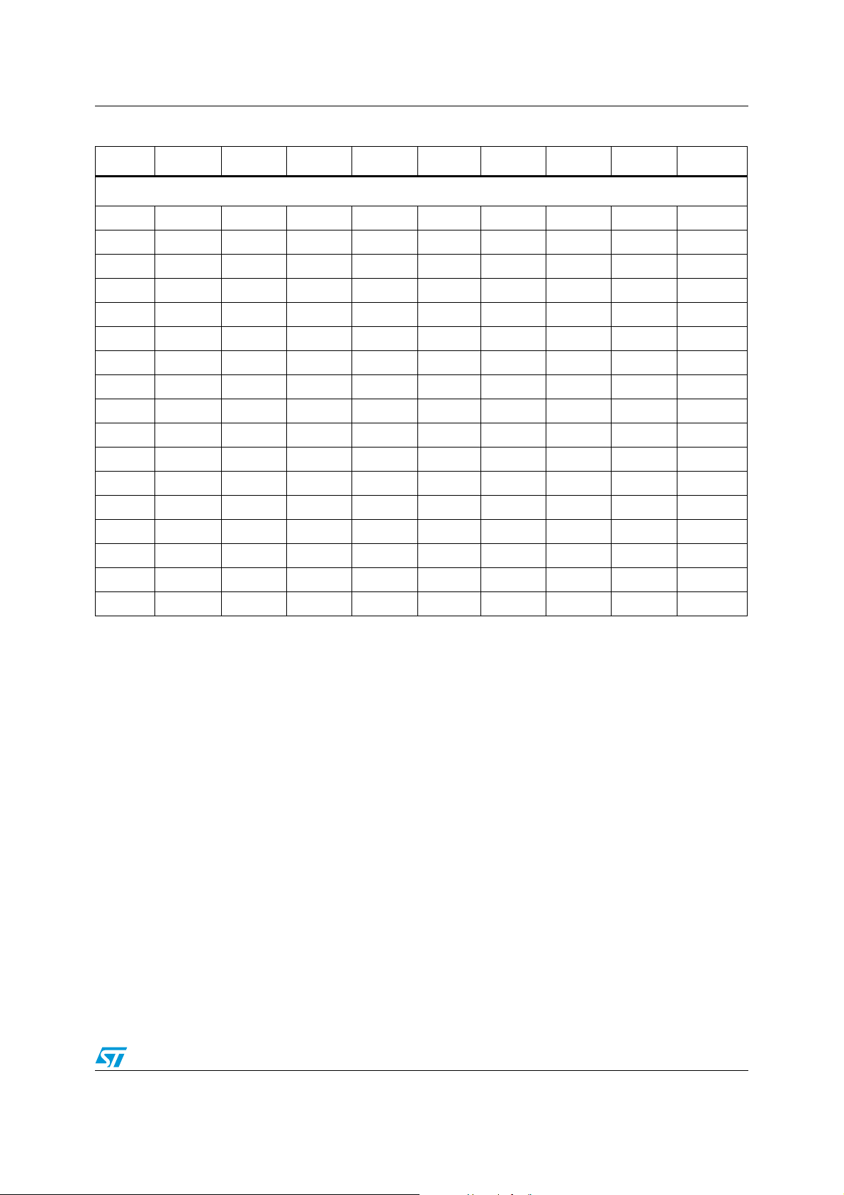
STA309B Registers
Table 8. Register summary (continued)
Addr Name D7 D6 D5 D4 D3 D2 D1 D0
Digital Pop-Free
0x57 PFCXON CH8 CH7 CH6 CH5 CH4 CH3 CH2 CH1
0x60Reserved--------
0x61Reserved--------
0x62Reserved--------
0x63Reserved--------
0x64Reserved--------
0x65Reserved--------
0x66 RAMPTIM TR7 TR6 TR5 TR4 TR3 TR2 TR1 TR0
0x67 TSPUPT1 TP15 TP14 TP13 TP12 TP11 TP10 TP9 TP8
0x68 TSPUPT0 TP7 TP6 TP5 TP4 TP3 TP2 TP1 TP0
0x69Reserved--------
0x6AReserved--------
0x6BReserved--------
0x6CReserved--------
0x70Reserved--------
0x71 LSPDWT1 TL15 TL14 TL13 TL12 TL11 TL10 TL9 TL8
0x72 LSPDWT0 TL7 TL6 TL5 TL4 TL3 TL2 TL1 TL
Doc ID 022570 Rev 2 21/66
Page 22
Registers STA309B
7.2 Register description
7.2.1 Configuration register A (0x00)
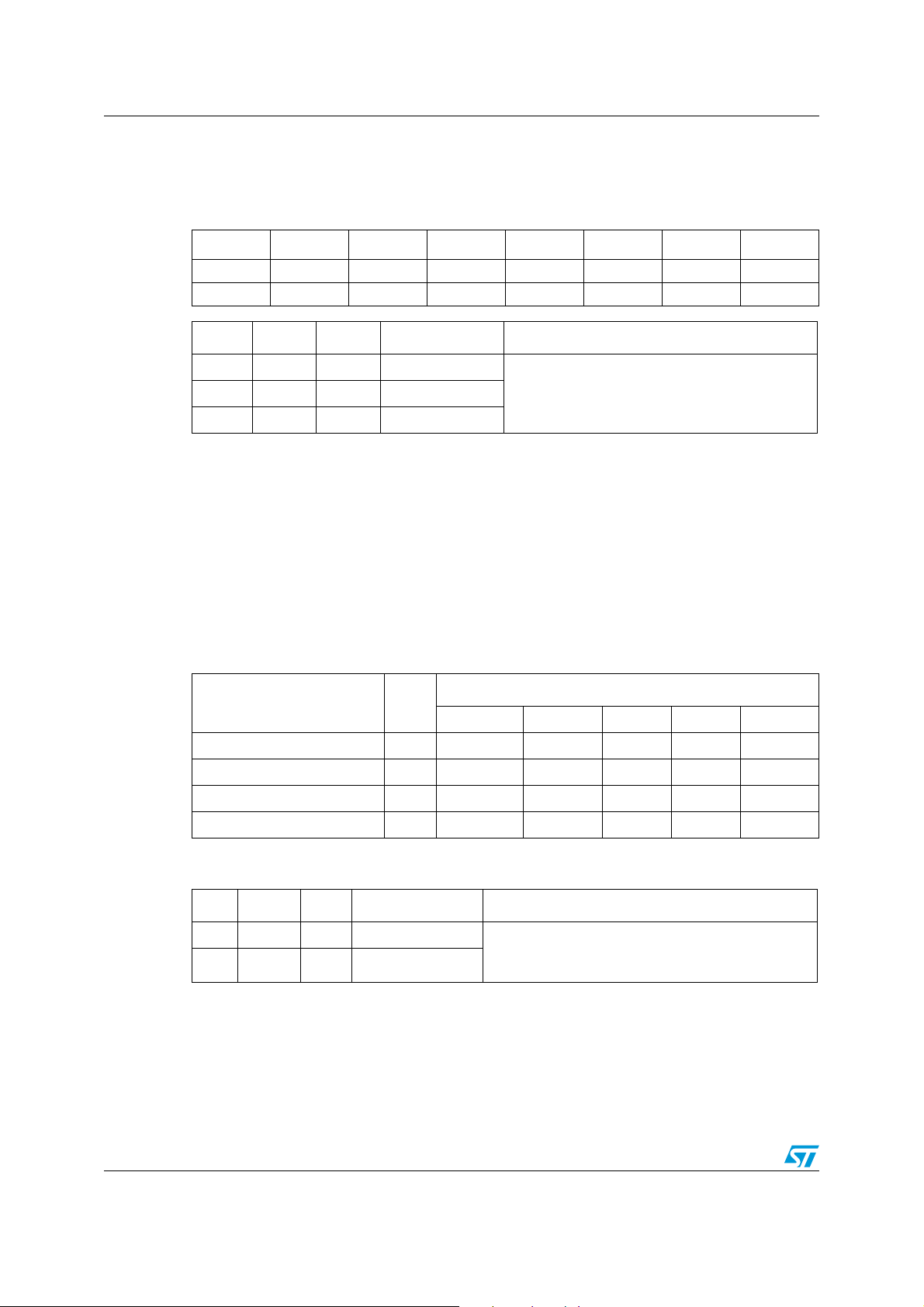
D7 D6 D5 D4 D3 D2 D1 D0
COS1 COS0 DSPB IR1 IR0 MCS2 MCS1 MCS0
10000011
Bit RW RST Name Description
0RW1 MCS0
1RW1 MCS1
2RW0 MCS2
The STA309B supports sampling rates of 32 kHz, 44.1 kHz, 48 kHz, 88.2 kHz, 96 kHz,
176.4 kHz, 192 kHz, and 2.8224 MHz DSD. Therefore the internal clocks are:
● 65.536 MHz for 32 kHz
● 90.3168 MHz for 44.1 kHz, 88.2 kHz, 176.4 kHz, and DSD
● 98.304 MHz for 48 kHz, 96 kHz, and 192 kHz
Master clock select: selects the ratio between the
input I2S sampling frequency and the input clock
The external clock frequency provided to the XTI pin must be a multiple of the input
sampling frequency (fs). The relationship between the input clock and the input sampling
rate is determined by both the MCSn and the IRn (input rate) register bits. The MCSn bits
determine the PLL factor generating the internal clock and the IRn bits determine the
oversampling ratio used internally.
Input sampling rate
fs (kHz)
IR
1XX 011 010 001 000
MCS[2:0]
32, 44.1, 48 00 128 * fs 256 * fs 384 * fs 512 * fs 768 * fs
88.2, 96 01 64 * fs 128 * fs 192 * fs 256 * fs 384 * fs
176.4, 192 10 64 * fs 128 * fs 192 * fs 256 * fs 384 * fs
DSD 11 2 * fs 4 * fs 6 * fs 8 * fs 10 * fs
Interpolation ratio select
Bit RW RST Name Description
3 RW 0 IR0 Interpolation ratio select: selects internal
interpolation ratio based on input I
4RW 0 IR1
frequency
The STA309B has variable interpolation (oversampling) settings such that internal
processing and FFX output rates remain consistent. The first processing block interpolates
by either 4 times, 2 times, or 1 time (pass-through).
2
S sampling
The oversampling ratio of this interpolation is determined by the IR bits.
22/66 Doc ID 022570 Rev 2
Page 23
STA309B Registers
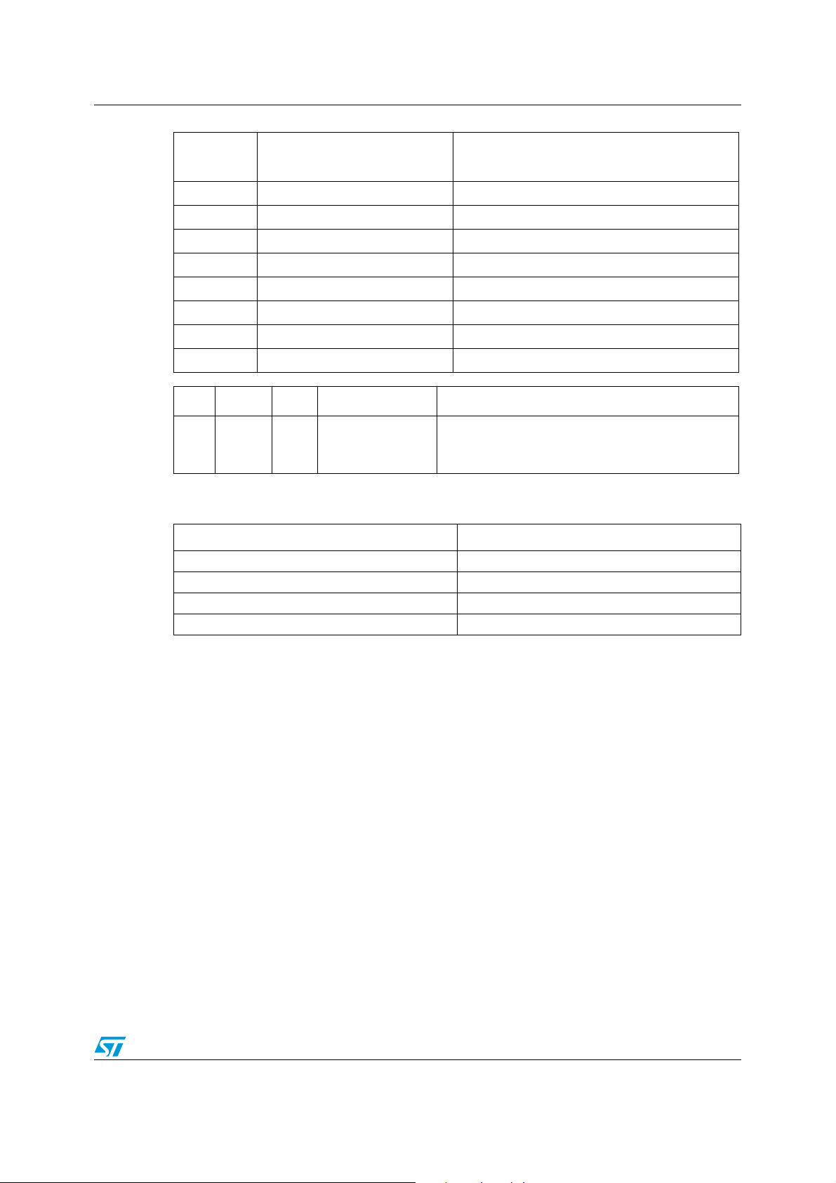
I
IR[1,0]
Input sampling rate
Fs (kHz)
1st stage interpolation ratio
00 32 4-times oversampling
00 44.1 4-times oversampling
00 48 4-times oversampling
01 88.2 2-times oversampling
01 96 2-times oversampling
10 176.4 Pass-through
10 192 Pass-through
11 DSD DSD to 176.4 kHz conversion
Bit RW RST Name Description
DSP bypass bit:
0 RW 0 DSPB
0: normal operation
1: bypass of biquad and bass/treble functions
Setting the DSPB bit bypasses the biquad function of the FFX core.
COS[1,0] CKOUT frequency
00 PLL output
01 PLL output / 4
10 PLL output / 8
11 PLL output / 16
Doc ID 022570 Rev 2 23/66
Page 24
Registers STA309B
7.2.2 Configuration register B (0x01) - serial input formats
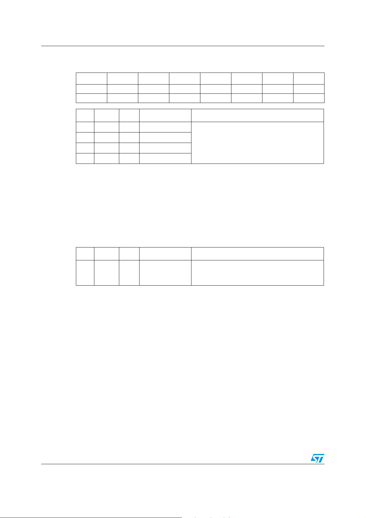
D7 D6 D5 D4 D3 D2 D1 D0
SAIFB SAI3 SAI2 SAI1 SAI0
00000
Bit RW RST Name Description
0 RW 0 SAI0
1 RW 0 SAI1
2 RW 0 SAI2
3 RW 0 SAI3
Serial data interface
The STA309B audio serial input interfaces with standard digital audio components and
accepts a number of serial data formats. The STA309B always acts a slave when receiving
audio input from standard digital audio components. Serial data for eight channels is
provided using 6 input pins: left/right clock LRCKI (pin 10), serial clock BICKI (pin 11), serial
data 1 and 2 SDI12 (pin 9), serial data 3 and 4 SDI34 (pin 8), serial data 5 and 6 SDI56 (pin
7), and serial data 7 and 8 SDI78 (pin 6). The SAI/SAIFB register (configuration register B,
address 0x01) is used to specify the serial data format. The default serial data format is I
MSB-first. Available formats are shown in the tables that follow.
Bit RW RST Name Description
Serial audio input interface format: determines the
interface format of the input serial digital audio
interface.
2
S,
Determines MSB or LSB first for all SAO formats:
4 RW 0 SAIFB
0: MSB first
1: LSB first
Note: Serial input and output formats are specified separately
For example, SAI = 1110 and SAIFB = 1 specifies right-justified 16-bit data, LSB-first.
24/66 Doc ID 022570 Rev 2
Page 25
STA309B Registers
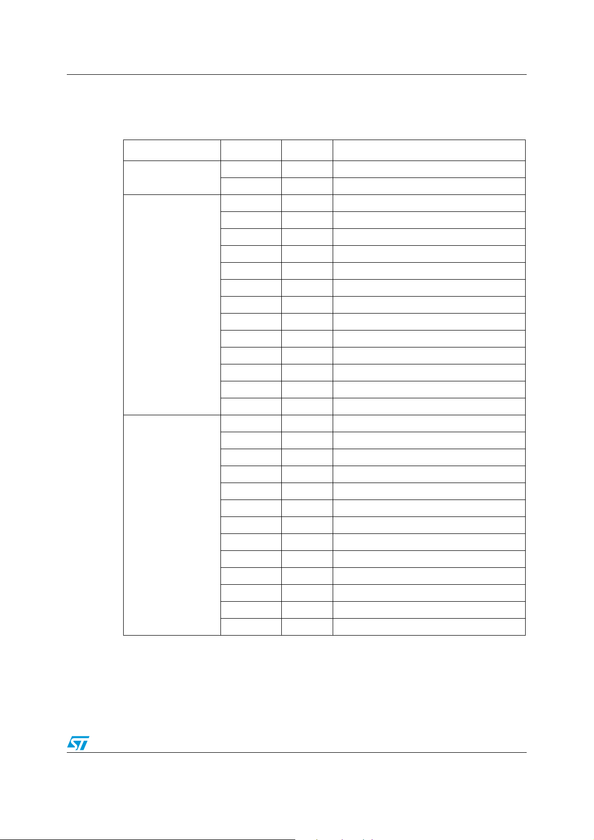
The table below lists the serial audio input formats supported by the STA309B as related to
BICKI = 32
* fs, 48 * fs, 64 * fs, where sampling rate, fs = 32, 44.1, 48, 88.2, 96, 176.4,
192 kHz.
BICKI SAI [3:0] SAIFB Interface format
32 * fs
1100 X I
1110 X Left/right-justified 16-bit data
0100 X I
0100 X I
1000 X I
0100 0 MSB-first I
1100 1 LSB-first I
0001 X Left-justified 24-bit data
2
S 15-bit data
2
S 23-bit data
2
S 20-bit data
2
S 18-bit data
2
2
S 16-bit data
S 16-bit data
48 * fs
64 * fs
0101 X Left-justified 20-bit data
1001 X Left-justified 18-bit data
1101 X Left-justified 16-bit data
0010 X Right-justified 24-bit data
0110 X Right-justified 20-bit data
1010 X Right-justified 18-bit data
1110 X Right-justified 16-bit data
2
0000 X I
0100 X I
1000 X I
0000 0 MSB-first I
1100 1 LSB-first I
S 24-bit data
2
S 20-bit data
2
S 18-bit data
2
2
S 16-bit data
S 16-bit data
0001 X Left-justified 24-bit data
0101 X Left-justified 20-bit data
1001 X Left-justified 18-bit data
1101 X Left-justified 16-bit data
0010 X Right-justified 24-bit data
0110 X Right-justified 20-bit data
1010 X Right-justified 18-bit data
1110 X Right-justified 16-bit data
Doc ID 022570 Rev 2 25/66
Page 26
Registers STA309B
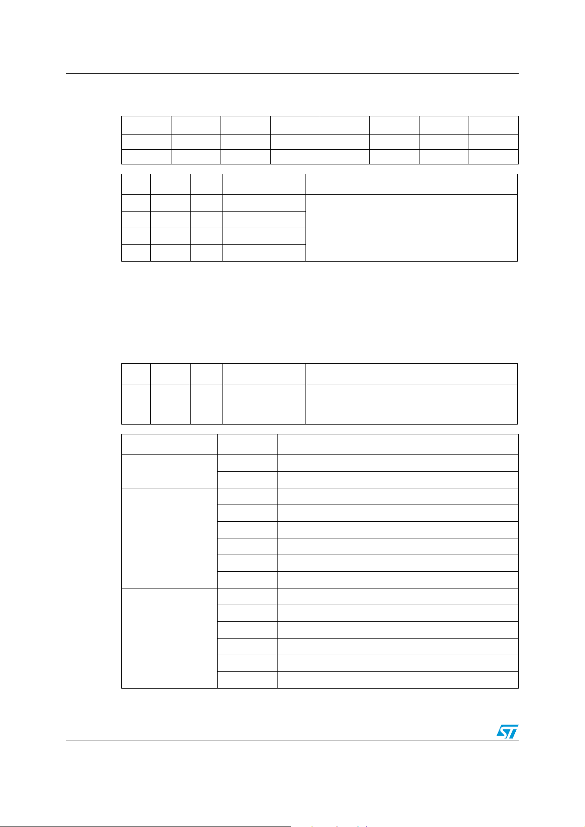
7.2.3 Configuration register C (0x02) - serial output formats
D7 D6 D5 D4 D3 D2 D1 D0
SAOFB SAO3 SAO2 SAIO SAO0
00000
Bit RW RST Name Description
0RW 0 SAO0
1RW 0 SAO1
2RW 0 SAO2
3RW 0 SAO3
The STA309B features a serial audio output interface that consists of 8 channels. The serial
audio output always acts as a slave to the serial audio input interface and, therefore, all
output clocks are synchronous with the input clocks. The output sampling frequency (fs) is
also equivalent to the input sampling frequency. In the case of SACD/DSD and PDM input,
the serial audio output acts as a master with an output sampling frequency of 176.4 kHz.
The output serial format can be selected independently from the input format and is done
via the SAO and SAOFB bits.
Bit RW RST Name Description
Serial audio output interface format: determines the
interface format of the output serial digital audio
interface.
Determines MSB or LSB first for all SAO formats:
4RW 0 SAOFB
0: MSB first
1: LSB first
BICKI = BICKO SAO[3:0] Interface data format
2
0111 I
S data
32 * fs
1111 Left/right-justified 16-bit data
1110 I
2
S data
0001 Left-justified data
1010 Right-justified 24-bit data
48 * fs
1011 Right-justified 20-bit data
1100 Right-justified 18-bit data
1101 Right-justified 16-bit data
0000 I
2
S data
0001 Left-justified data
0010 Right-justified 24-bit data
64 * fs
0011 Right-justified 20-bit data
0100 Right-justified 18-bit data
0101 Right-justified 16-bit data
26/66 Doc ID 022570 Rev 2
Page 27
STA309B Registers
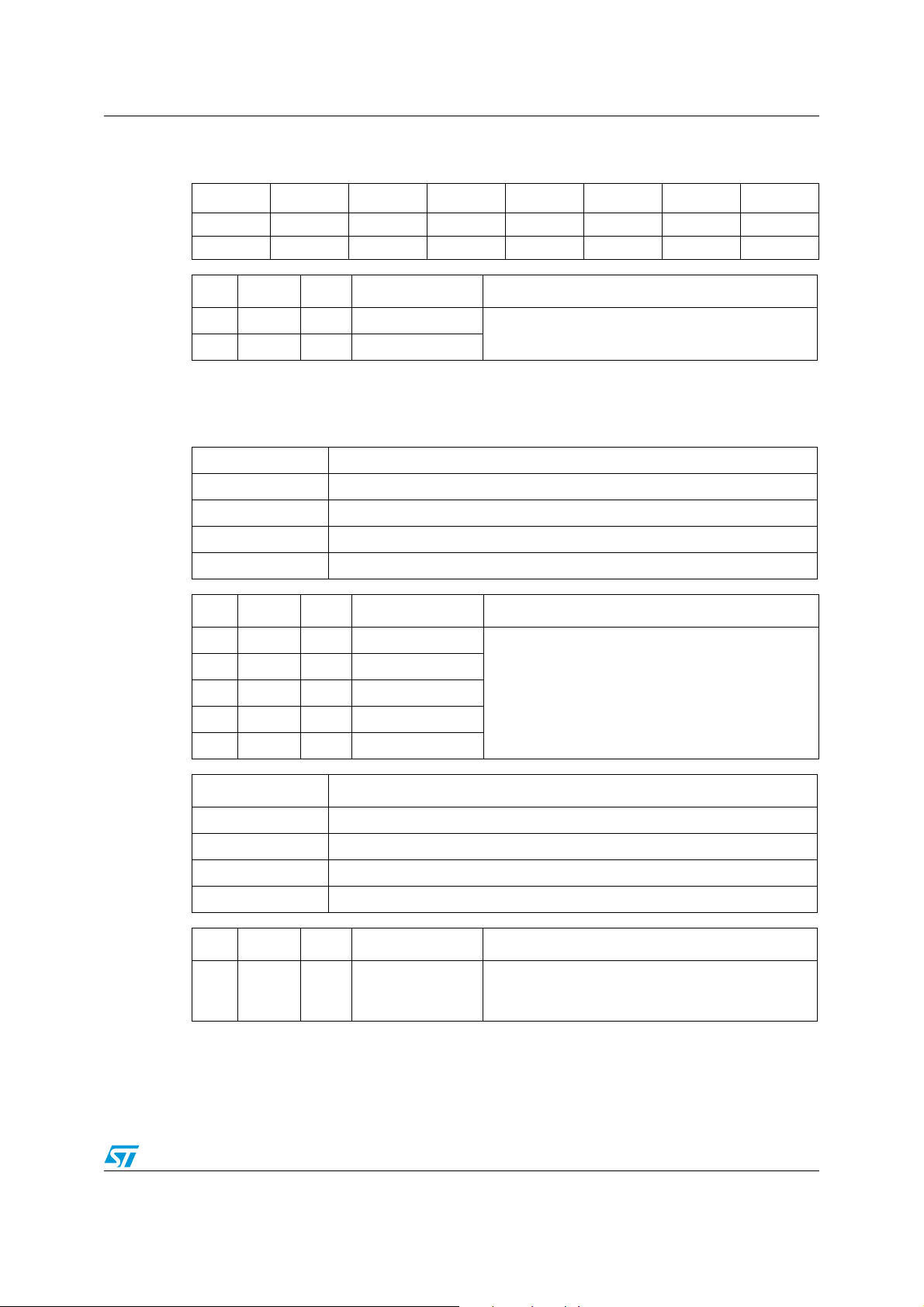
7.2.4 Configuration register D (0x03)
D7 D6 D5 D4 D3 D2 D1 D0
MPC CSZ4 CSZ3 CSZ2 CSZ1 CSZ0 OM1 OM0
11000010
Bit RW RST Name Description
0RW 0 OM0
1RW 1 OM1
FFX power output mode: selects configuration of
FFX output
The FFX power output mode selects how the FFX output timing is configured. Different
power devices use different output modes. The STA50x recommended use is
OM = 10.
OM[1,0] Output stage - mode
00 STA50x/STA51xB - drop compensation
01 Discrete output stage - tapered compensation
10 STA50x/STA51xB - full power mode
11 Variable drop compensation (CSZn bits)
Bit RW RST Name Description
2RW 0 CSZ0
3RW 0 CSZ1
4RW 0 CSZ2
5RW 0 CSZ3
6RW 1 CSZ4
CSZ[4:0] Compensating pulse size
Contra size register: when OM[1,0] = 11, this register
determines the size of the FFX compensating pulse
from 0 clock ticks to 31 clock periods.
00000 0 clock period compensating pulse size
00001 1 clock period compensating pulse size
……
11111 31 clock period compensating pulse size
Bit RW RST Name Description
Max power correction: setting to 1 enables STA50x
7RW 1 MPC
correction for THD reduction near maximum power
output
Setting the MPC bit turns on special processing that corrects the STA50x power device at
high power. This mode should lower the THD+N of a full STA50x FFX system at maximum
power output and slightly below. This mode will only be operational at OM[1,0] = 01.
Doc ID 022570 Rev 2 27/66
Page 28
Registers STA309B
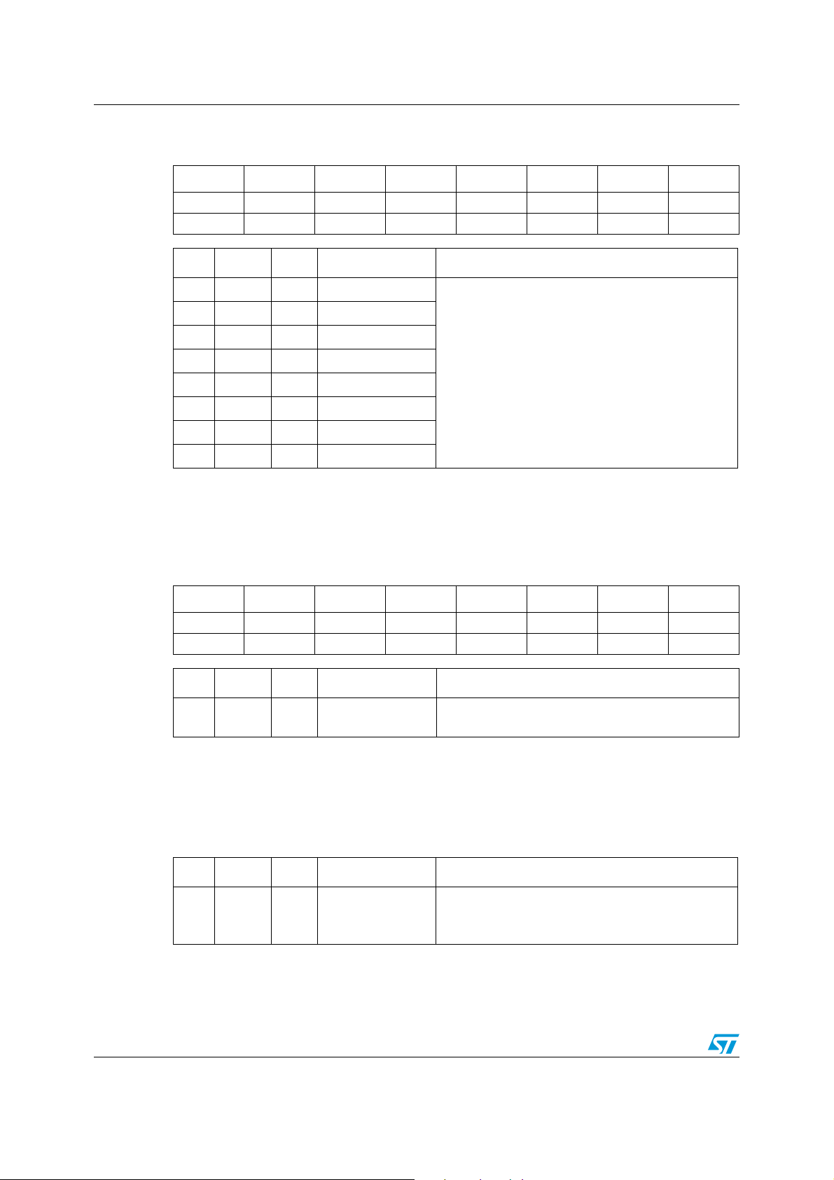
7.2.5 Configuration register E (0x04)
D7 D6 D5 D4 D3 D2 D1 D0
C8BO C7BO C6BO C5BO C4BO C3BO C2BO C1BO
00000000
Bit RW RST Name Description
0RW 0 C1BO
1RW 0 C2BO
2RW 0 C3BO
3RW 0 C4BO
4RW 0 C5BO
5RW 0 C6BO
6RW 0 C7BO
7RW 0 C8BO
Each individual channel output can be set to output a binary PWM stream. In this mode
output A of a channel will be considered the positive output and output B is the negative
inverse.
Channels 1, 2, 3, 4, 5, 6, 7, and 8 binary output
mode enable bits. A setting of 0 indicates ordinary
FFX tristate output. A setting of 1 indicates binary
output mode
7.2.6 Configuration register F (0x05)
D7 D6 D5 D4 D3 D2 D1 D0
PWMS2 PWMS1 PWMS0 BQL PSL DEMP DRC HPB
00000000
Bit RW RST Name Description
0RW 0 HPB
The STA309B features an internal digital high-pass filter for the purpose of AC coupling. The
purpose of this filter is to prevent DC signals from passing through an FFX amplifier. DC
signals can cause speaker damage.
If HPB = 1, then the filter that the high-pass filter utilizes is made available as userprogrammable biquad #1.
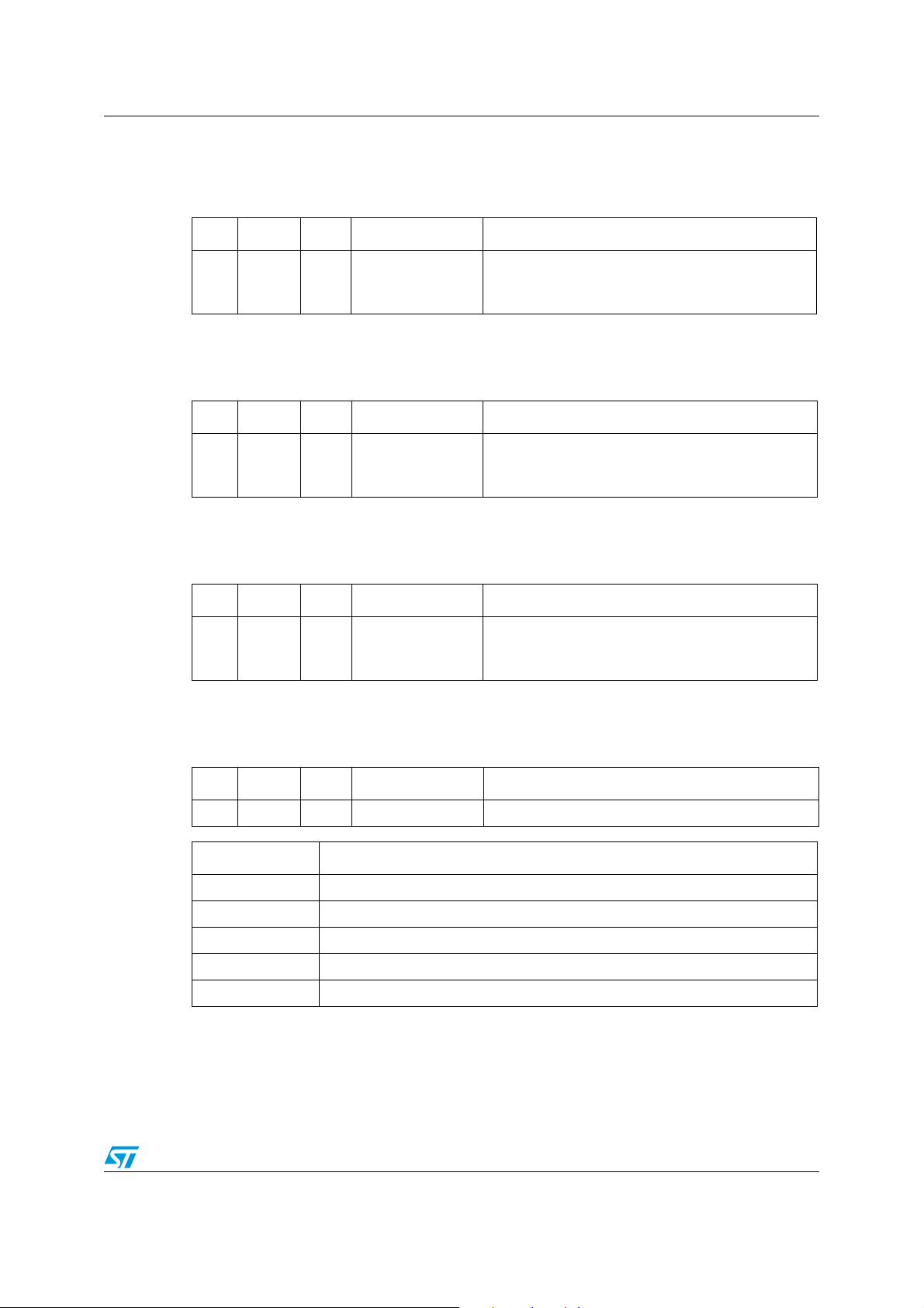
Bit RW RST Name Description
1 RW 0 DRC
Both limiters can be used in one of two ways, anti-clipping or dynamic range compression.
When used in anti-clipping mode the limiter threshold values are constant and dependent on
the limiter settings.
High-pass filter bypass bit: setting to one bypasses
the internal AC coupling digital high-pass filter
Dynamic range compression/anti-clipping
0: limiters act in anti-clipping mode
1: limiters act in dynamic range compression mode
28/66 Doc ID 022570 Rev 2
Page 29
STA309B Registers
In dynamic range compression mode the limiter threshold values vary with the volume
settings allowing a nighttime listening mode that provides a reduction in the dynamic range
regardless of the volume level.
Bit RW RST Name Description
De-emphasis:
2RW 0 DEMP
0: no de-emphasis
1: de-emphasis
By setting this bit to one, de-emphasis will be implemented on all channels. When this is
used, it takes the place of biquad #7 in each channel and any coefficients using biquad #1
will be ignored. The DSPB (DSP bypass) bit must be set to 0 for de-emphasis to function.
Bit RW RST Name Description
Post-scale link:
3 RW 0 PSL
0: each channel uses individual post-scale value
1: each channel uses channel 1 post-scale value
Post-Scale functionality can be used for power-supply error correction. For multichannel
applications running off the same power supply, the post-scale values can be linked to the
value of channel 1 for ease of use and in order to update the values faster.
Bit RW RST Name Description
Biquad link:
4RW 0 BQL
0: each channel uses coefficient values
1: each channel uses channel 1 coefficient values
For ease of use, all channels can use the biquad coefficients loaded into the channel 1
coefficient RAM space by setting the BQL bit to 1. Therefore, any EQ updates only have to
be performed once.
Bit RW RST Name Description
7:5 RW 00 PWMS[2:0] PWM speed selection:
PWMS[1:0] PWM output speed
000 Normal speed (384 kHz) (all channels)
001 Half-speed (192 kHz) (all channels)
010 Double-speed (768 kHz) (all channels)
011 Normal speed (channels 1-6), double-speed (channels 7-8)
100 Odd speed (341.3 kHz) (all channels)
Doc ID 022570 Rev 2 29/66
Page 30
Registers STA309B
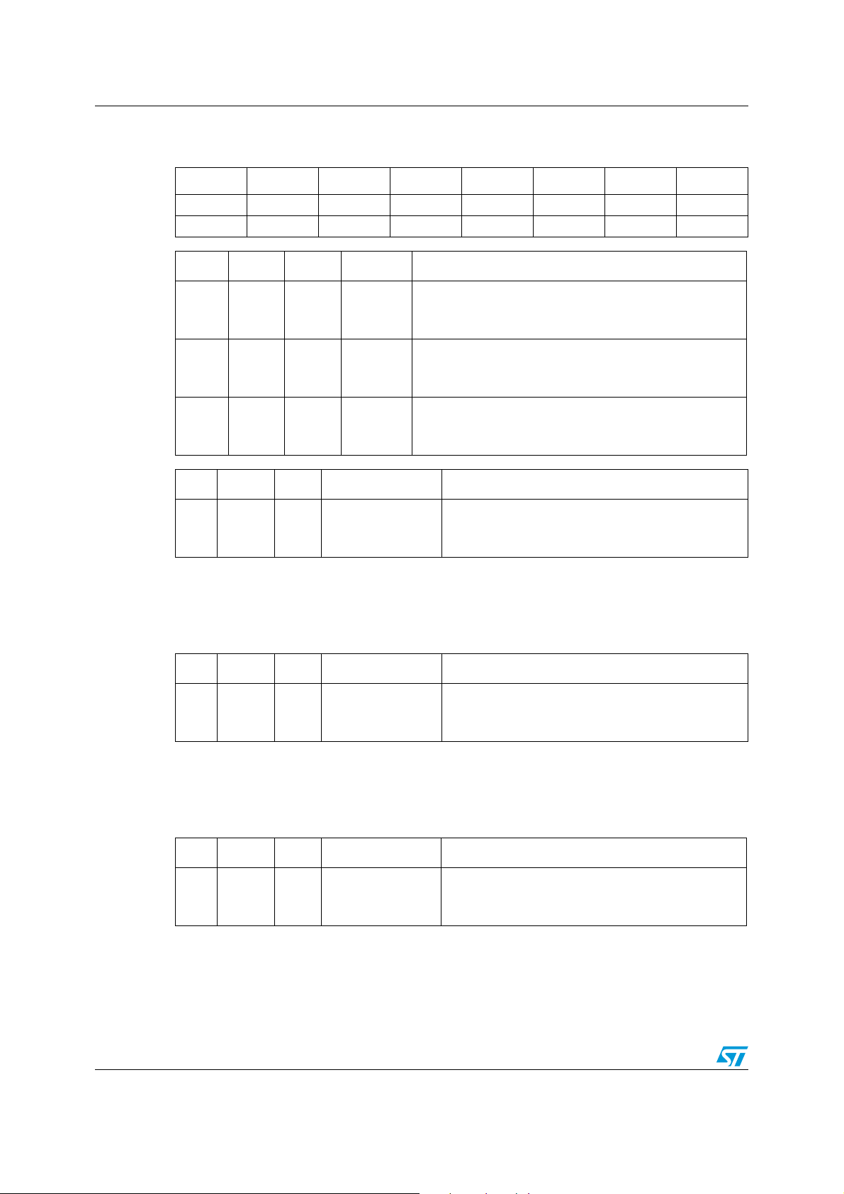
7.2.7 Configuration register G (0x06)
D7 D6 D5 D4 D3 D2 D1 D0
MPCV DCCV HPE AM2E AME COD SID PWMD
00000000
Bit RW RST Name Description
PWM output disable:
0RW0 PWMD
1RW0 SID
2RW0 COD
Bit RW RST Name Description
0: PWM output normal
1: no PWM output
2
Serial interface (I
2
S output normal
0: I
S out) disable:
1: no I2S output
Clock output disable:
0: clock output normal
1: no clock output
AM mode enable:
3RW 0 AME
0: normal FFX operation.
1: AM reduction mode FFX operation
The STA309B features an FFX processing mode that minimizes the amount of noise
generated in the frequency range of AM radio. This mode is intended for use when FFX is
operating in a device with an active AM tuner. The SNR of the FFX processing is reduced to
~83 dB in this mode, which is still greater than the SNR of AM radio.
Bit RW RST Name Description
AM2 mode enable:
4RW 0 AM2E
0: normal FFX operation
1: AM2 reduction mode FFX operation
The STA309B features 2 FFX processing modes that minimize the amount of noise
generated in the frequency range of AM radio. This second mode is intended for use when
FFX is operating in a device with an active AM tuner. This mode eliminates the noiseshaper.
Bit RW RST Name Description
FFX headphone enable:
5RW 0 HPE
0: channels 7 and 8 normal FFX operation
1: channels 7 and 8 headphone operation
Channels 7 and 8 can be configured to be processed and output in such a manner that
headphones can be driven using an appropriate output device. This signal is a differential
3-wire drive called FFX headphone.
30/66 Doc ID 022570 Rev 2
Page 31
STA309B Registers
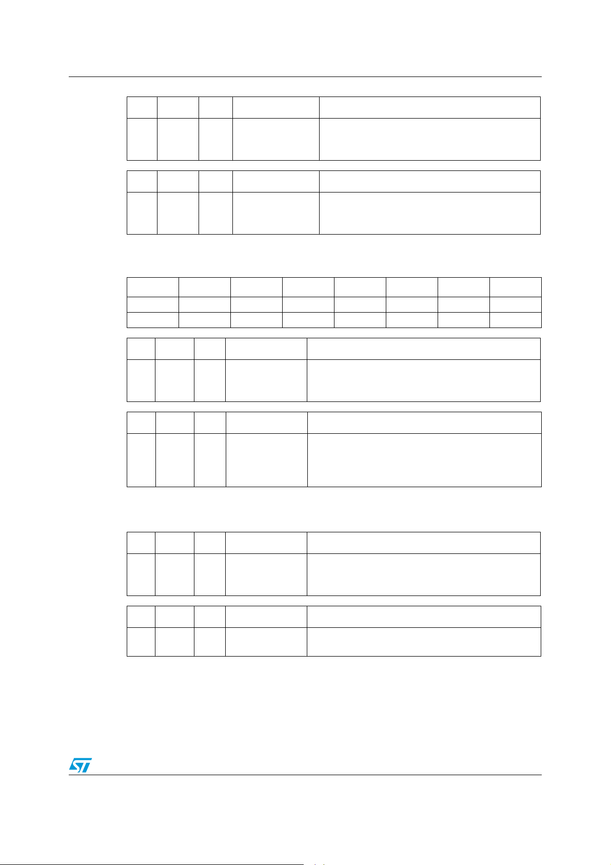
Bit RW RST Name Description
Distortion compensation variable enable:
6 RW 0 DCCV
0: uses preset DC coefficient
1: uses DCC coefficient
Bit RW RST Name Description
Max power correction variable:
7RW 0 MPCV
0: uses standard MPC coefficient
1: uses MPCC bits for MPC coefficient
7.2.8 Configuration register H (0x07)
D7 D6 D5 D4 D3 D2 D1 D0
ECLE LDTE BCLE IDE ZDE SVE ZCE NSBW
01111110
Bit RW RST Name Description
Noise-shaper bandwidth selection:
0 RW 0 NSBW
1: 3
rd
order NS
0: 4th order NS
Bit RW RST Name Description
Zero-crossing volume enable:
1RW1 ZCE
1: volume adjustments will only occur at digital zerocrossings
0: volume adjustments will occur immediately
The ZCE bit enables zero-crossing volume adjustments. When the volume is adjusted on
digital zero-crossings, no clicks will be audible.
Bit RW RST Name Description
Soft volume enable:
2RW1 SVE
Bit RW RST Name Description
3RW1 ZDE
1: volume adjustments use soft volume
0: volume adjustments occur immediately
Zero-detect mute enable: setting to 1 enables the
automatic zero-detect mute
Setting the ZDE bit enables the zero-detect automatic mute. The zero-detect circuit looks at
the input data of each processing channel after the channel-mapping block. If any channel
receives 2048 consecutive zero-value samples (regardless of fs), then that individual
channel is muted if this function is enabled.
Doc ID 022570 Rev 2 31/66
Page 32
Registers STA309B
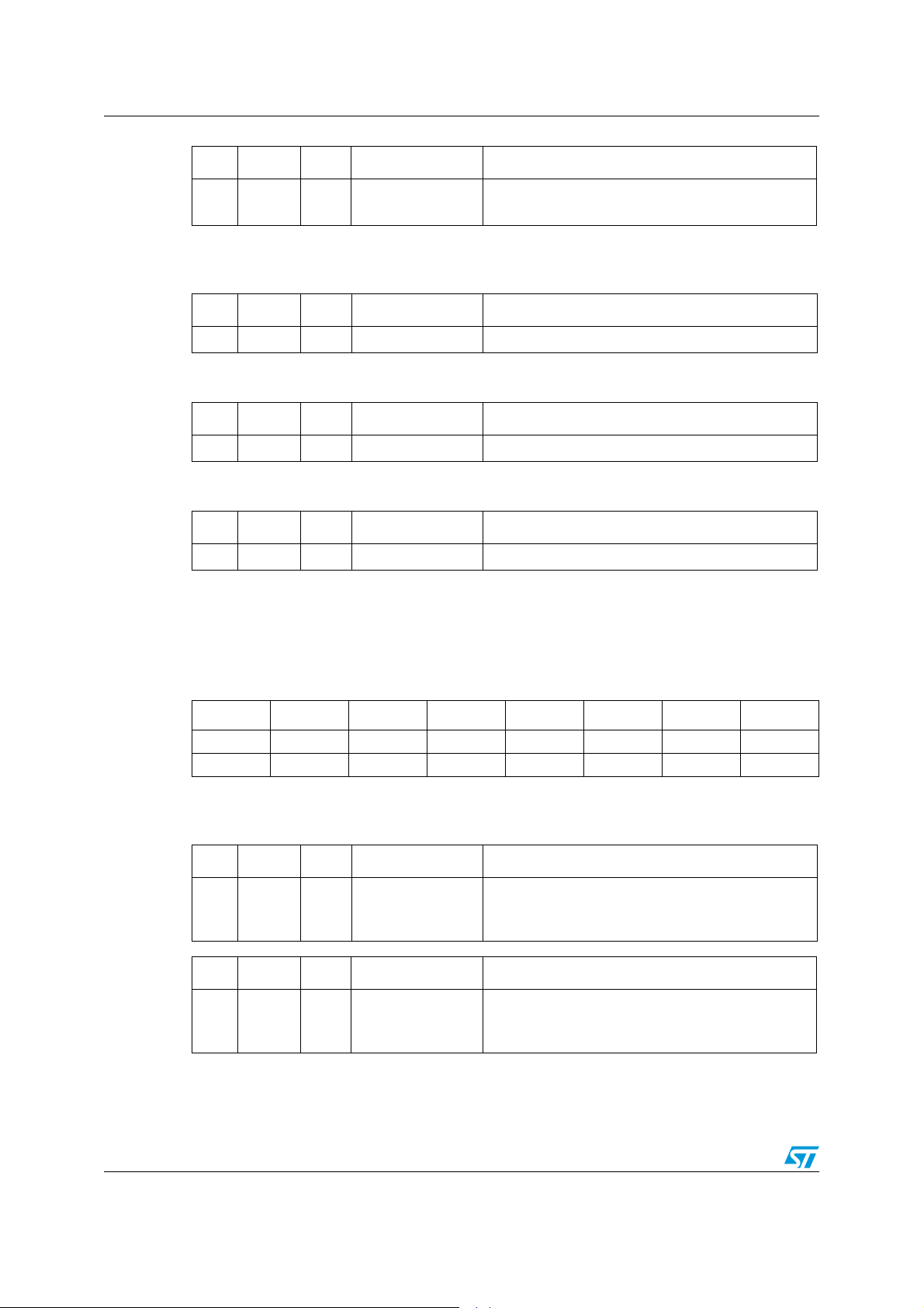
Bit RW RST Name Description
4RW 1 IDE
Invalid input detect mute enable:
1: enables the automatic invalid input detect mute
Setting the IDE bit enables this function, which looks at the input I2S data and will
automatically mute if the signals are perceived as invalid.
Bit RW RST Name Description
5 RW 1 BCLE Binary output mode clock loss detection enable
This function detects loss of input MCLK in binary mode and will output 50% duty cycle.
Bit RW RST Name Description
6 RW 1 LDTE LRCLK double triggering protection enable
This function actively prevents double triggering of LRCLK.
Bit RW RST Name Description
7 RW 1 ECLE Auto EAPD on clock loss
Device power-down signal (EAPD) on clock loss detection. This function is enabled by
default. It is strongly recommended to avoid spurious noise during the on-off sequence. The
STA309B has the ECLE bit set to 0.
7.2.9 Configuration register I (0x08)
D7 D6 D5 D4 D3 D2 D1 D0
EAPD PSCE
0 0
This feature utilizes an ADC on SDI78 that provides power supply ripple information for
correction. Registers PSC1, PSC2, PSC3 are utilized in this mode.
Bit RW RST Name Description
0 RW 0 PSCE
Bit RW RST Name Description
7 RW 0 EAPD
Power supply ripple correction enable:
0: normal operation
1: PSCorrect operation
External amplifier power-down:
0: external power-stage power-down active
1: normal operation
32/66 Doc ID 022570 Rev 2
Page 33
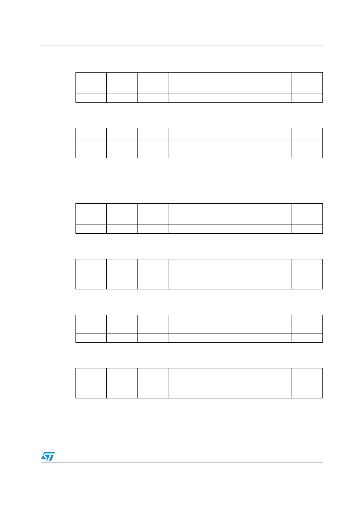
STA309B Registers
7.2.10 Master mute register (0x09)
D7 D6 D5 D4 D3 D2 D1 D0
MMUTE
0
7.2.11 Master volume register (0x0A)
D7 D6 D5 D4 D3 D2 D1 D0
MV7 MV6 MV5 MV4 MV3 MV2 MV1 MV0
11111111
Note: The value of the volume derived from MVOL is dependent on the AMV AutoMode volume
settings.
7.2.12 Channel 1 volume (0x0B)
D7 D6 D5 D4 D3 D2 D1 D0
C1V7 C1V6 C1V5 C1V4 C1V3 C1V2 C1V1 C1V0
01100000
7.2.13 Channel 2 volume (0x0C)
D7 D6 D5 D4 D3 D2 D1 D0
C2V7 C2V6 C2V5 C2V4 C2V3 C2V2 C2V1 C2V0
01100000
7.2.14 Channel 3 volume (0x0D)
D7 D6 D5 D4 D3 D2 D1 D0
C3V7 C3V6 C3V5 C3V4 C3V3 C3V2 C3V1 C3V0
01100000
7.2.15 Channel 4 volume (0x0E)
D7 D6 D5 D4 D3 D2 D1 D0
C4V7 C4V6 C4V5 C4V4 C4V3 C4V2 C4V1 C4V0
01100000
Doc ID 022570 Rev 2 33/66
Page 34
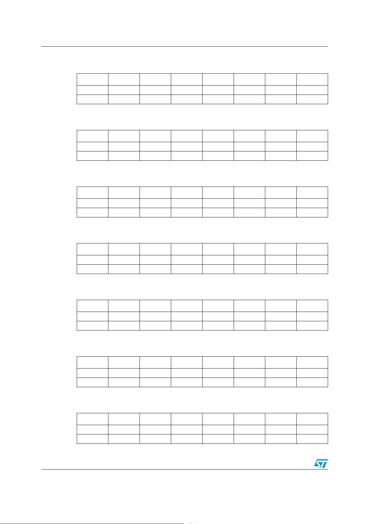
Registers STA309B
7.2.16 Channel 5 volume (0x0F)
D7 D6 D5 D4 D3 D2 D1 D0
C5V7 C5V6 C5V5 C5V4 C5V3 C5V2 C5V1 C5V0
01100000
7.2.17 Channel 6 volume (0x10)
D7 D6 D5 D4 D3 D2 D1 D0
C6V7 C6V6 C6V5 C6V4 C6V3 C6V2 C6V1 C6V0
01100000
7.2.18 Channel 7 volume (0x11)
D7 D6 D5 D4 D3 D2 D1 D0
C7V7 C7V6 C7V5 C7V4 C7V3 C7V2 C7V1 C7V0
01100000
7.2.19 Channel 8 volume (0x12)
D7 D6 D5 D4 D3 D2 D1 D0
C8V7 C8V6 C8V5 C8V4 C8V3 C8V2 C8V1 C8V0
01100000
7.2.20 Channel 1 volume trim, mute, bypass (0x13)
D7 D6 D5 D4 D3 D2 D1 D0
C1M C1VBP C1VT4 C1VT3 C1VT2 C1VT1 C1VT0
00010000
7.2.21 Channel 2 volume trim, mute, bypass (0x14)
D7 D6 D5 D4 D3 D2 D1 D0
C2M C2VBP C2VT4 C2VT3 C2VT2 C2VT1 C2VT0
00010000
7.2.22 Channel 3 volume trim, mute, bypass (0x15)
D7 D6 D5 D4 D3 D2 D1 D0
C3M C3VBP C3VT4 C3VT3 C3VT2 C3VT1 C3VT0
00010000
34/66 Doc ID 022570 Rev 2
Page 35
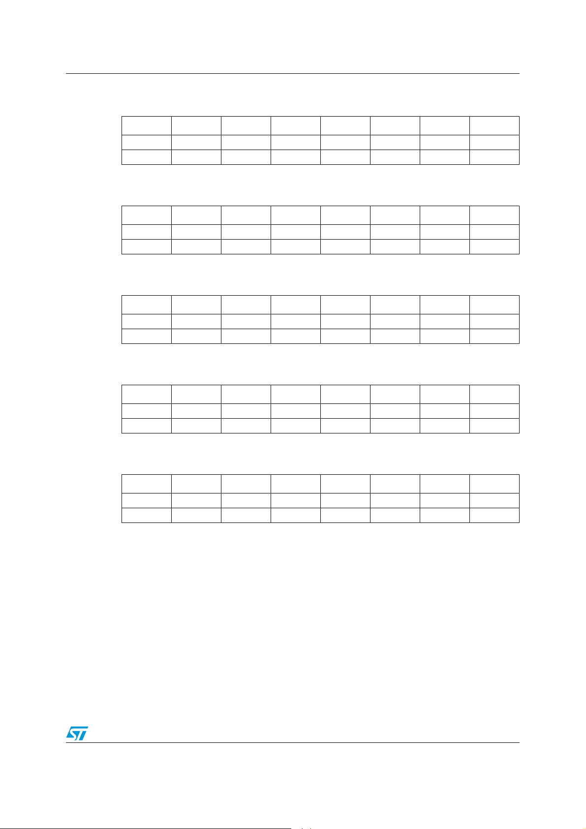
STA309B Registers
7.2.23 Channel 4 volume trim, mute, bypass (0x16)
D7 D6 D5 D4 D3 D2 D1 D0
C4M C4VBP C4VT4 C4VT3 C4VT2 C4VT1 C4VT0
00010000
7.2.24 Channel 5 volume trim, mute, bypass (0x17)
D7 D6 D5 D4 D3 D2 D1 D0
C5M C5VBP C5VT4 C5VT3 C5VT2 C5VT1 C5VT0
00010000
7.2.25 Channel 6 volume trim, mute, bypass (0x18)
D7 D6 D5 D4 D3 D2 D1 D0
C6M C6VBP C6VT4 C6VT3 C6VT2 C6VT1 C6VT0
00010000
7.2.26 Channel 7 volume trim, mute, bypass (0x19)
D7 D6 D5 D4 D3 D2 D1 D0
C7M C7VBP C7VT4 C7VT3 C7VT2 C7VT1 C7VT0
00010000
7.2.27 Channel 8 volume trim, mute, bypass (0x1A)
D7 D6 D5 D4 D3 D2 D1 D0
C8M C8VBP C8VT4 C8VT3 C8VT2 C8VT1 C8VT0
00010000
The volume structure of the STA309B consists of individual volume registers for each
channel and a master volume register that provides an offset to each channel’s volume
setting. There is also an additional offset for each channel called the channel volume trim.
The individual channel volumes are adjustable in 0.5 dB steps from +48 dB to -78 dB. As an
example if C5V = 0xXX or +XXX dB and MV = 0xXX or -XX dB, then the total gain for
channel 5 = XX dB. The channel volume trim is adjustable independently on each channel
from -10 dB to +10 dB in 1 dB steps. The master mute when set to 1 will mute all channels
at once, whereas the individual channel mutes (CnM) will mute only that channel. Both the
master mute and the channel mutes provide a "soft mute" with the volume ramping down to
mute in 8192 samples from the maximum volume setting at the internal processing rate
(~192 kHz). A "hard mute" can be obtained by commanding a value of 0xFF (255) to any
channel volume register or the master volume register. When volume offsets are provided
via the master volume register, any channel whose total volume is less than -91 dB will be
muted. All changes in volume take place at zero-crossings when ZCE = 1 (configuration
register H) on a per-channel basis as this creates the smoothest possible volume
Doc ID 022570 Rev 2 35/66
Page 36
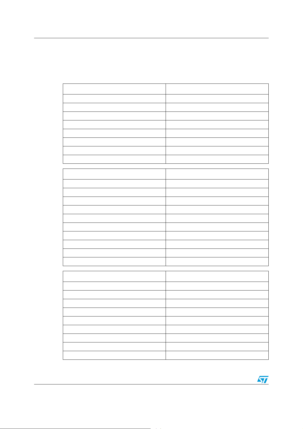
Registers STA309B
transitions. When ZCE = 0, volume updates occur immediately. Each channel also contains
an individual channel volume bypass. If a particular channel has volume bypassed via the
CnVBP = 1 register, then only the channel volume setting for that particular channel affects
the volume setting, the master volume setting will not affect that channel. Each channel also
contains a channel mute. If CnM = 1, a soft mute is performed on that channel.
MV[7:0] Volume offset from channel value
0x00 0 dB
0x01 -0.5 dB
0x02 -1 dB
……
0x4C -38 dB
……
0xFE -127 dB
0xFF Hardware channel mute
CnV[7:0] Volume
0x00 +48 dB
0x01 +47.5 dB
0x02 +47 dB
……
0x5F +0.5 dB
0x60 0 dB
0x61 -0.5 dB
……
0xFE -79.5 dB
0xFF Hardware channel mute
CnVT[4:0] Volume
0x00 to 0x06 +10 dB
0x07 +9 dB
……
0x0F +1 dB
0x10 0 dB
0x11 -1 dB
……
0x19 -9 dB
0x1A to 0x1F -10 dB
36/66 Doc ID 022570 Rev 2
Page 37
STA309B Registers
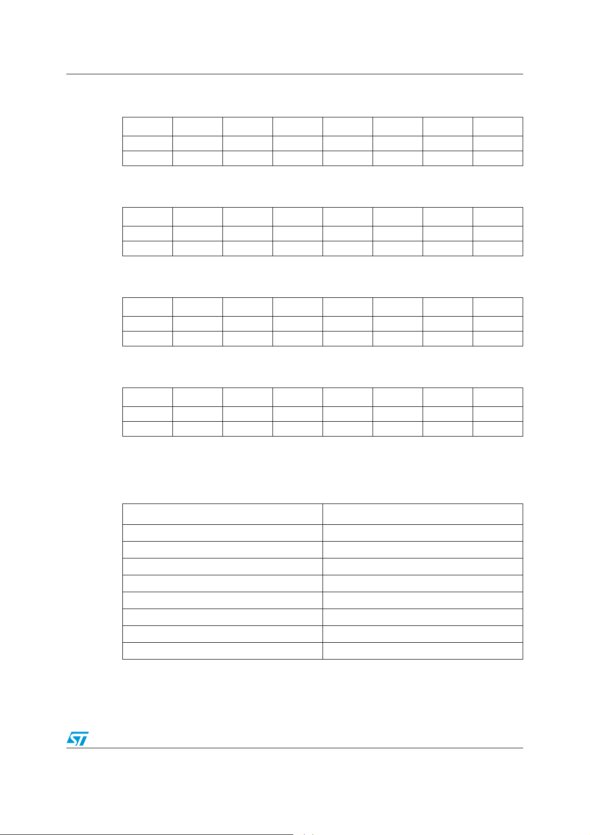
7.2.28 Channel input mapping channels 1 and 2 (0x1B)
D7 D6 D5 D4 D3 D2 D1 D0
C2IM2 C2IM1 C2IM0 C1IM2 C1IM1 C1IM0
001 000
7.2.29 Channel input mapping channels 3 and 4 (0x1C)
D7 D6 D5 D4 D3 D2 D1 D0
C4IM2 C4IM1 C4IM0 C3IM2 C3IM1 C3IM0
011 010
7.2.30 Channel input mapping channels 5 and 6 (0x1D)
D7 D6 D5 D4 D3 D2 D1 D0
C6IM2 C6IM1 C6IM0 C5IM2 C5IM1 C5IM0
101 100
7.2.31 Channel input mapping channels 7 and 8 (0x1E)
D7 D6 D5 D4 D3 D2 D1 D0
C8IM2 C8M1 C8IM0 C7IM2 C7IM1 C7IM0
111 110
Each channel received via I2S can be mapped to any internal processing channel via the
channel input mapping registers. This allows for flexibility in processing, simplifies output
stage designs, and enables the ability to perform crossovers. The default settings of these
registers map each I
000 Channel 1
001 Channel 2
010 Channel 3
011 Channel 4
100 Channel 5
101 Channel 6
110 Channel 7
111 Channel 8
2
S input channel to its corresponding processing channel.
CnIM[2:0] Serial input from
Doc ID 022570 Rev 2 37/66
Page 38
Registers STA309B
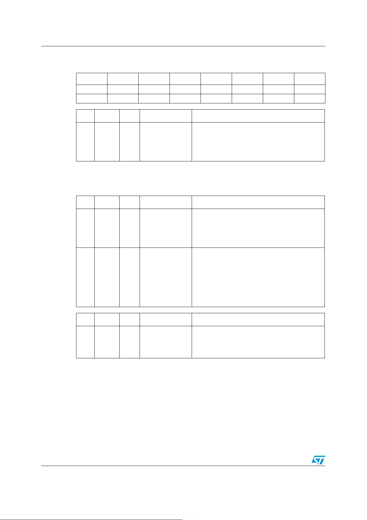
7.2.32 AUTO1 - AutoModes EQ, volume, GC (0x1F)
D7 D6 D5 D4 D3 D2 D1 D0
AMDM AMGC2 AMGC1 AMGC0 AMV1 AMV0 AMEQ1 AMEQ0
00000000
Bit RW RST Name Description
Biquad 2-6 mode is:
00: user-programmable
1:0 RW 0 AMEQ[1:0]
By setting AMEQ to any setting other than 00 enables AutoMode EQ, biquads 1-5 are not
user programmable. Any coefficient settings for these biquads will be ignored. Also when
AutoMode EQ is used, the pre-scale value for channels 1-6 becomes hard-set to -18 dB.
Bit RW RST Name Description
3:2 RW 0 AMV[1:0]
6:4 RW 0 AMGC[2:0]
Bit RW RST Name Description
01: preset EQ - PEQ bits
10: graphic EQ - xGEQ bits
11: auto volume controlled loudness curve
AutoMode volume mode (MVOL) is:
00: MVOL 0.5 dB 256 steps (standard)
01: MVOL auto curve 30 steps
10: MVOL auto curve 40 steps
11: MVOL auto curve 50 steps
AutoMode gain compression/limiters mode is:
000: user programmable GC
001: AC no clipping
010: AC limited clipping (10%)
011: DRC nighttime listening mode
100: DRC TV commercial/channel AGC
101: AC 5.1 no clipping
110: AC 5.1 limited clipping (10%)
AutoMode 5.1 downmix:
7RW 0 AMDM
0: normal operation
1: channels 7-8 are 2-channel downmix of channels
1-6
The AutoMode downmix setting uses channels 7-8 of Mix#1 engine and therefore these
channels of this function are fixed and not allowed to be set by the user when in this mode.
Channels 1-6 must be arranged via channel mapping (registers CnIM), if necessary, in the
following manner for this operation:
Channel 1: left
Channel 2: right
Channel 3: left surround
Channel 4: right surround
Channel 5: center
Channel 6: LFE
38/66 Doc ID 022570 Rev 2
Page 39
STA309B Registers
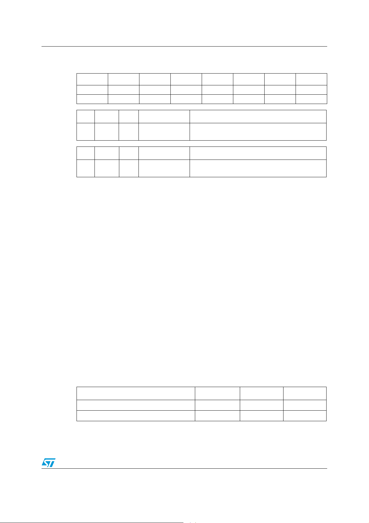
7.2.33 AUTO2 - AutoModes bass management2 (0x20)
D7 D6 D5 D4 D3 D2 D1 D0
SUB RSS1 RSS0 CSS1 CSS0 FSS AMBMXE AMBMME
10000000
Bit RW RST Name Description
0 RW 0 AMBMME
0: AutoMode bass management mix disabled
1: AutoMode bass management mix enabled
Bit RW RST Name Description
1 RW 0 AMBMXE
0: AutoMode bass management crossover disabled
1: AutoMode bass management crossover enabled
Setting the AMBMME bit enables the proper mixing to take place for various preset bass
management configurations. Setting the AMBMXE bit enables the proper crossover filtering
in biquad #7 to take place. The crossover for bass management is always 2
nd
order
(24 dB/oct) and the crossover frequency is determined by register bits PREEQ.XO[2:0].
All configurations of Dolby Bass Management can be performed in the IC. These different
configurations are selected as they would be by the end-user.
The AutoMode bass management settings utilize channels 1-6 in the Mix #1 engine,
Channels 1-6 biquad #6, and channels 1-2 in the mix #2 engine in configuration #2. These
functions cannot be user-programmed while the bass management automode is active.
Not all settings are valid as some configurations are unlikely and do not have to be
supported by Dolby specifications.
Automatic crossover settings are provided or custom crossovers can be implemented using
the available programmable biquads.
Input channels must be mapped using the channel-mapping feature in the following manner
for bass management to be performed properly.
1: left front
2: right front
3: left rear
4: right rear
5: center
6: LFE
Bitfield 10 01 00
CSS - center speaker size Off Large Small
RSS - rear speaker size Off Large Small
Doc ID 022570 Rev 2 39/66
Page 40
Registers STA309B
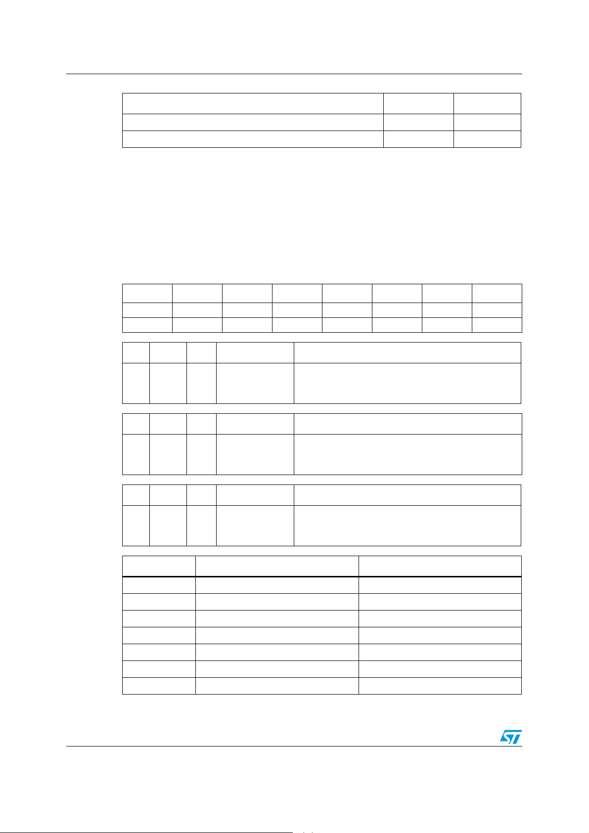
Bitfield 1 0
FSS - front speaker size Large Small
SUB - subwoofer On Off
When AMBMXE = 1, biquad #7 on channels 1-6 are utilized for the bass-management
crossover filter, this biquad is not user-programmable in this mode. The XO settings
determine the crossover frequency used, the crossover is 2
nd
order for both high-pass and
low-pass with a -3 dB cross point. Higher order filters can be obtained be programming
coefficients in other biquads if desired.
It is recommended to use settings of 120-160 Hz when using small, single driver satellite
speakers as the frequency response of these speakers normally is limited to this region.
7.2.34 AUTO3 - AutoMode AM/pre-scale/bass management scale (0x21)
D7 D6 D5 D4 D3 D2 D1 D0
AMAM2 AMAM1 AMAM0 AMAME MSA AMPS
0000 00
Bit RW RST Name Description
AutoMode pre-scale
0RW0 AMPS
0: -18 dB used for pre-scale when AMEQ = 00
1: user-defined pre-scale when AMEQ = 00
Bit RW RST Name Description
Bass management mix scale adjustment
1RW0 MSA
0: -12 dB scaling on satellite channels in config #1
1: no scaling on satellite channels in config #1
Bit RW RST Name Description
AutoMode AM enable
4RW0 AMAME
0: switching frequency determined by PWMS settings
1: switching frequency determined by AMAM settings
AMAM[2:0] 48 kHz/96 kHz input Fs 44.1 / 88.2 kHz input Fs
000 0.535 MHz - 0.720 MHz 0.535 MHz - 0.670 MHz
001 0.721 MHz - 0.900 MHz 0.671 MHz - 0.800 MHz
010 0.901 MHz - 1.100 MHz 0.801 MHz - 1.000 MHz
011 1.101 MHz - 1.300 MHz 1.001 MHz - 1.180 MHz
100 1.301 MHz - 1.480 MHz 1.181 MHz - 1.340 MHz
101 1.481 MHz - 1.600 MHz 1.341 MHz - 1.500 MHz
110 1.601 MHz - 1.700 MHz 1.501 MHz - 1.700 MHz
40/66 Doc ID 022570 Rev 2
Page 41
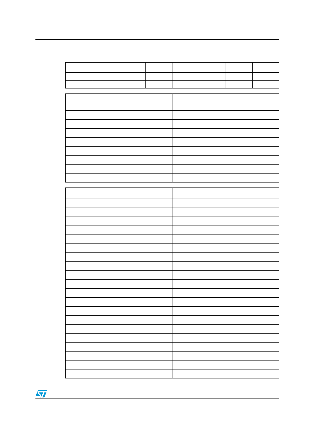
STA309B Registers
7.2.35 PREEQ - preset EQ settings (0x22)
D7 D6 D5 D4 D3 D2 D1 D0
XO2 XO1 XO0 PEQ4 PEQ3 PEQ2 PEQ1 PEQ0
10100000
XO[2:0]
000 70 Hz
001 80 Hz
010 90 Hz
011 100 Hz
100 110 Hz
101 120 Hz
110 140 Hz
111 160 Hz
PEQ[4:0] Mode / setting
Bass management
crossover frequency
00000 Flat
00001 Rock
00010 Soft Rock
00011 Jazz
00100 Classical
00101 Dance
00110 Pop
00111 Soft
01000 Hard
01001 Party
01010 Vocal
01011 Hip-Hop
01100 Dialog
01101 Bass-boost #1
01110 Bass-boost #2
01111 Bass-boost #3
10000 Loudness 1
10001 Loudness 2
10010 Loudness 3
10011 Loudness 4
Doc ID 022570 Rev 2 41/66
Page 42
Registers STA309B
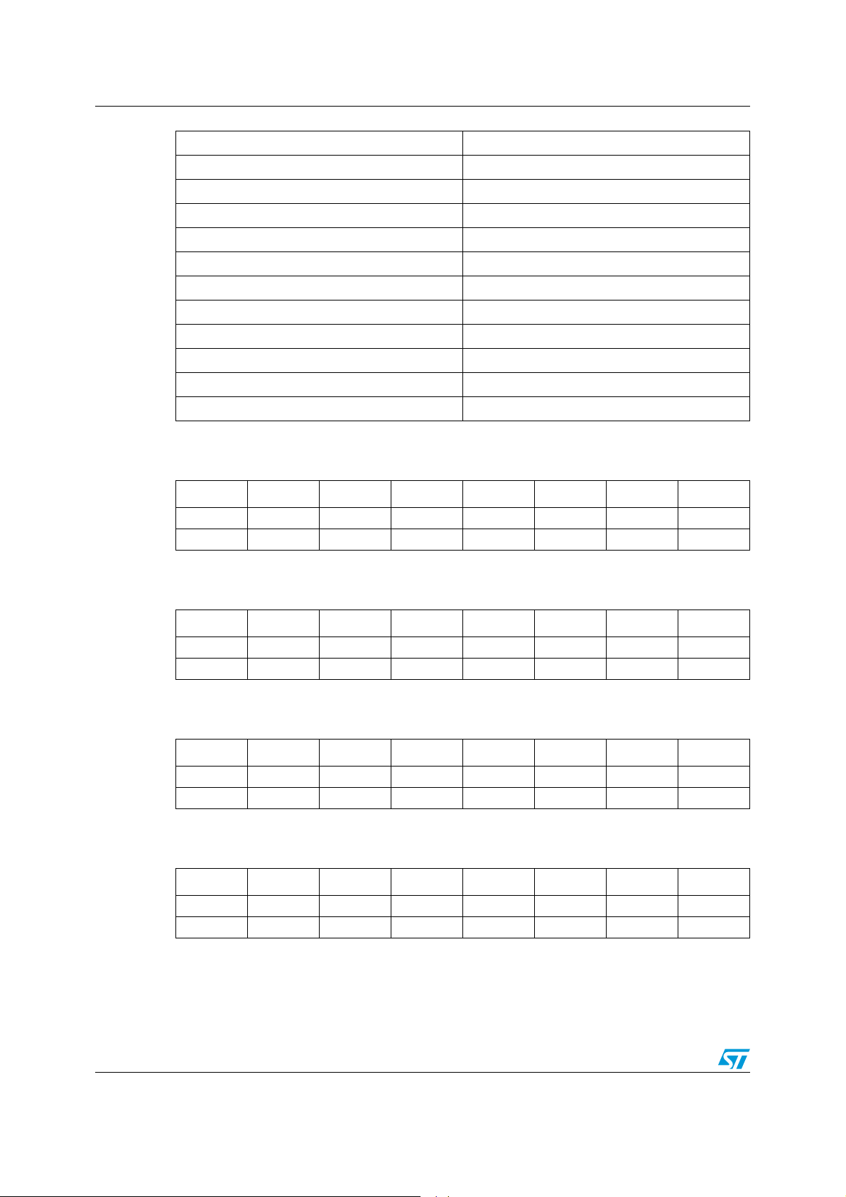
10100 Loudness 5
10101 Loudness 6
10110 Loudness 7
10111 Loudness 8
11000 Loudness 9
11001 Loudness 10
11010 Loudness 11
11011 Loudness 12
11100 Loudness 13
11101 Loudness 14
11110 Loudness 15
11111 Loudness 16
7.2.36 AGEQ - graphic EQ 80-Hz band (0x23)
D7 D6 D5 D4 D3 D2 D1 D0
AGEQ4 AGEQ3 AGEQ2 AGEQ1 AGEQ0
01111
7.2.37 BGEQ - graphic EQ 300-Hz band (0x24)
D7 D6 D5 D4 D3 D2 D1 D0
BGEQ4 BGEQ3 BGEQ2 BGEQ1 BGEQ0
01111
7.2.38 CGEQ - graphic EQ 1-kHz band (0x25)
D7 D6 D5 D4 D3 D2 D1 D0
CGEQ4 CGEQ3 CGEQ2 CGEQ1 CGEQ0
01111
7.2.39 DGEQ - graphic EQ 3-kHz band (0x26)
D7 D6 D5 D4 D3 D2 D1 D0
DGEQ4 DGEQ3 DGEQ2 DGEQ1 DGEQ0
01111
42/66 Doc ID 022570 Rev 2
Page 43
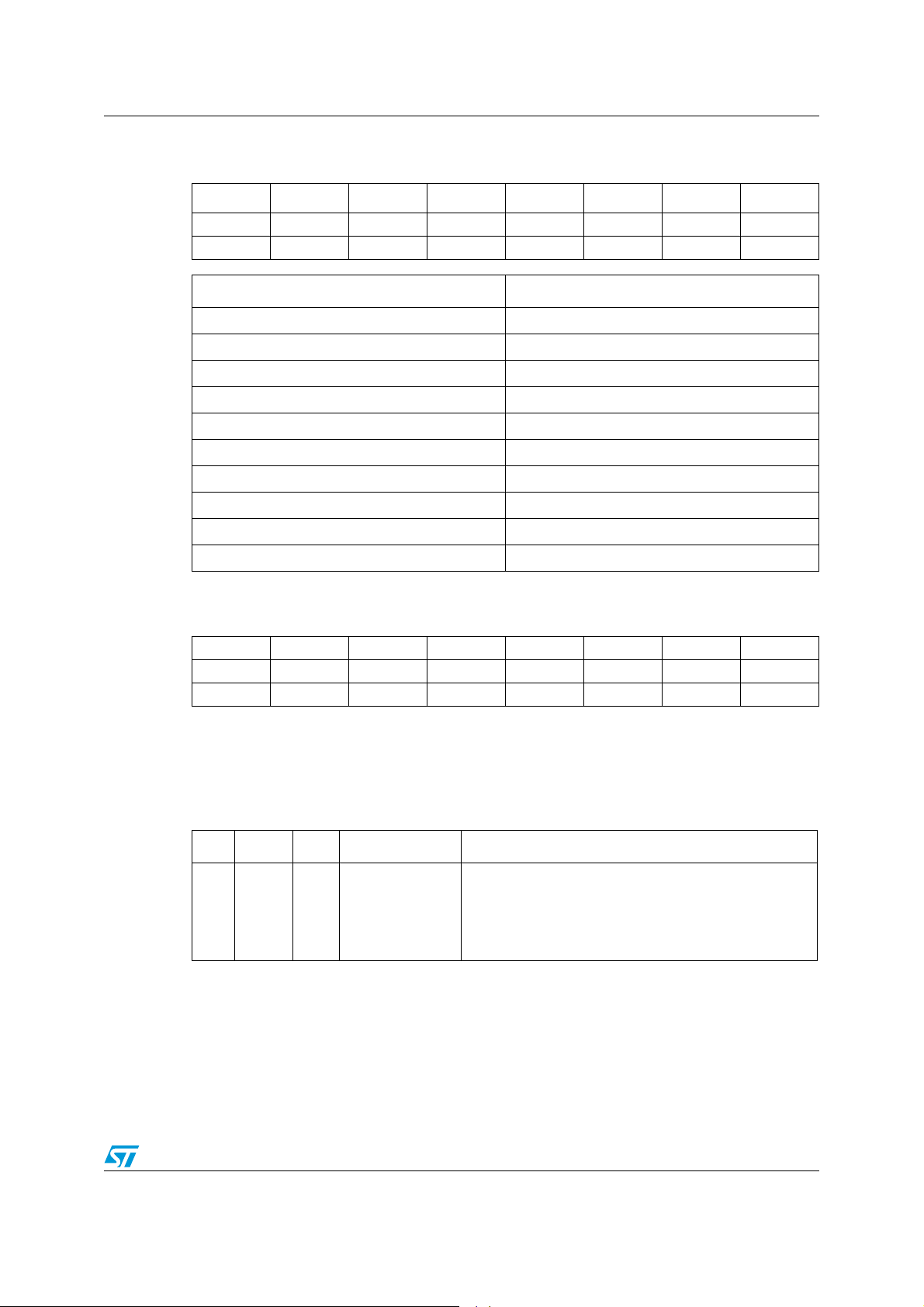
STA309B Registers
7.2.40 EGEQ - graphic EQ 8-kHz band (0x27)
D7 D6 D5 D4 D3 D2 D1 D0
EGEQ4 EGEQ3 EGEQ2 EGEQ1 EGEQ0
01111
xGEQ[4:0] Boost / cut
11111 +16
11110 +15
11101 +14
……
10000 +1
01111 0
01110 -1
……
00001 -14
00000 -15
7.2.41 Biquad internal channel loop-through (0x28)
D7 D6 D5 D4 D3 D2 D1 D0
C8BLP C7BLP C6BLP C5BLP C4BLP C3BLP C2BLP C1BLP
00000000
Each internal processing channel can receive two possible inputs at the input to the biquad
block. The input can come either from the output of that channel’s MIX#1 engine or from the
output of the bass/treble (biquad #10) of the previous channel. In this scenario, channel 1
receives channel 8. This enables the use of more than 10 biquads on any given channel at
the expense of losing the number of separate internal processing channels.
Bit RW RST Name Description
For n = 1 to 8:
0: input from channel n MIX#1 engine output - normal
7:0 RW 0 CnBLP
operation
1: input from channel (n - 1) biquad #10 output - loop
operation
Doc ID 022570 Rev 2 43/66
Page 44
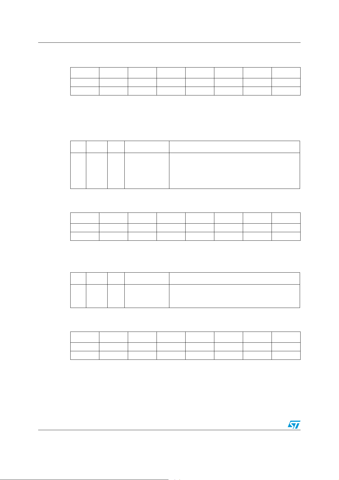
Registers STA309B
7.2.42 Mix internal channel loop-through (0x29)
D7 D6 D5 D4 D3 D2 D1 D0
C8MXLP C7MXLP C6MXLP C5MXLP C4MXLP C3MXLP C2MXLP C1MXLP
00000000
Each internal processing channel can receive two possible sets of inputs at the inputs to the
Mix#1 block. The inputs can come from the outputs of the interpolation block as normally
occurs (CnMXLP = 0) or they can come from the outputs of the Mix#2 block. This enables
the use of additional filtering after the second mix block at the expense of losing this
processing capability on the channel.
Bit RW RST Name Description
For n = 1 to 8:
0: inputs to channel n MIX#1 engine from interpolation
7:0 RW 0 CnMXLP
outputs - normal operation
1: inputs to channel n MIX#1 engine from MIX#2 engine
outputs - loop operation
7.2.43 EQ bypass (0x2A)
D7 D6 D5 D4 D3 D2 D1 D0
C8EQBP C7EQBP C6EQBP C5EQBP C4EQCBP C3EQBP C2EQBP C1EQBP
00000000
EQ control can be bypassed on a per-channel basis. If EQ control is bypassed on a given
channel, the prescale and all 10 filters (high-pass, biquads, de-emphasis, bass
management crossover, bass, treble in any combination) are bypassed for that channel.
Bit RW RST Name Description
7:0 RW 0 CnEQBP
7.2.44 Tone control bypass (0x2B)
D7 D6 D5 D4 D3 D2 D1 D0
C8TCB C7TCB C6TCB C5TCB C4TCB C3TCB C2TCB C1TCB
00000000
Tone control (bass/treble) can be bypassed on a per-channel basis. If tone control is
bypassed on a given channel, the two filters that tone control utilizes are made available as
user-programmable biquads #9 and #10.
For n = 1 to 8:
0: perform EQ on channel n - normal operation
1: bypass EQ on channel n
44/66 Doc ID 022570 Rev 2
Page 45
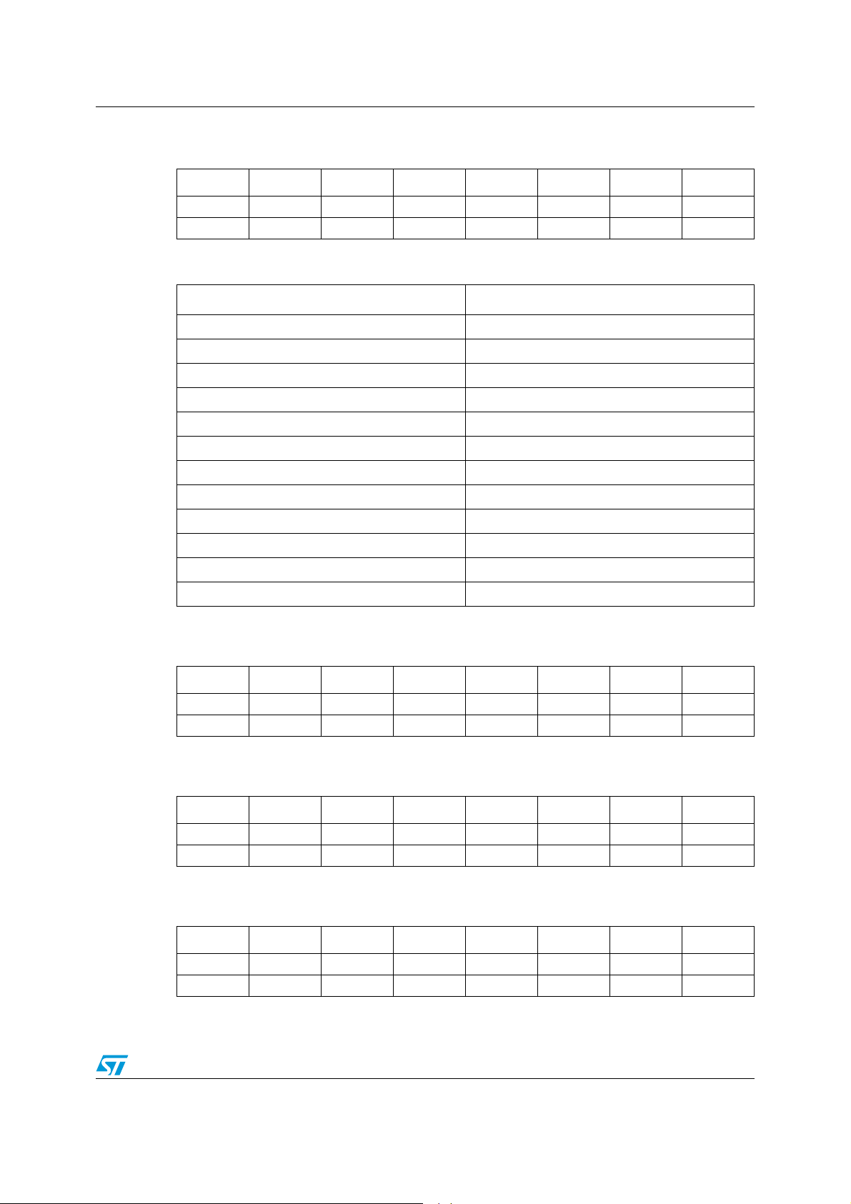
STA309B Registers
7.2.45 Tone control (0x2C)
D7 D6 D5 D4 D3 D2 D1 D0
TTC3 TTC2 TTC1 TTC0 BTC3 BTC2 BTC1 BTC0
01110111
This is the tone control boost / cut as a function of the BTC and TTC bits.
BTC[3:0] / TTC[3:0) Boost / cut
0000 -12 dB
0001 -12 dB
……
0111 -4 dB
0110 -2 dB
0111 0 dB
1000 +2 dB
1001 +4 dB
……
1101 +12 dB
1110 +12 dB
1111 +12dB
7.2.46 Channel limiter select channels 1,2,3,4 (0x2D)
D7 D6 D5 D4 D3 D2 D1 D0
C4LS1 C4LS0 C3LS1 C3LS0 C2LS1 C2LS0 C1LS1 C1LS0
00000000
7.2.47 Channel limiter select channels 5,6,7,8 (0x2E)
D7 D6 D5 D4 D3 D2 D1 D0
C8LS1 C8LS0 C7LS1 C7LS0 C6LS1 C6LS0 C5LS1 C5LS0
00000000
7.2.48 Limiter 1 attack/release rate (0x2F)
D7 D6 D5 D4 D3 D2 D1 D0
L1A3 L1A2 L1A1 L1A0 L1R3 L1R2 L1R1 L1R0
01101010
Doc ID 022570 Rev 2 45/66
Page 46
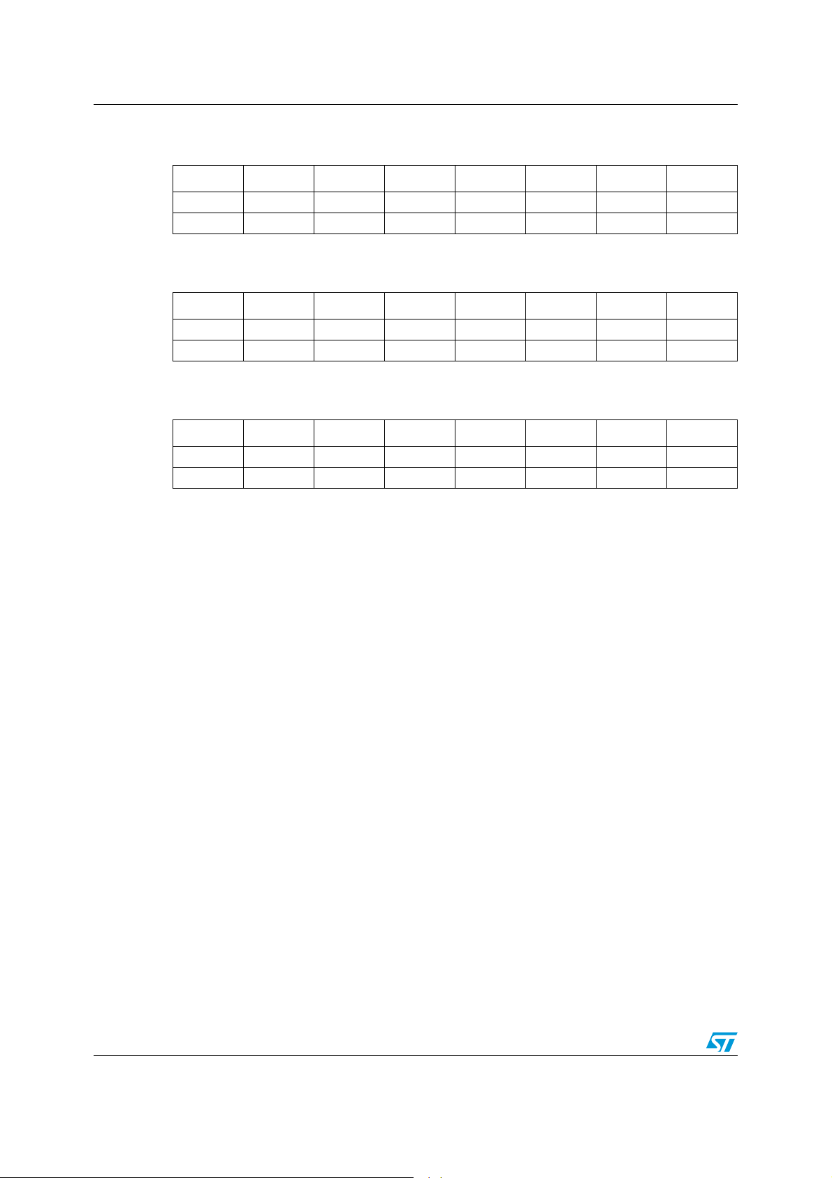
Registers STA309B
7.2.49 Limiter 1 attack/release threshold (0x30)
D7 D6 D5 D4 D3 D2 D1 D0
L1AT3 L1AT2 L1AT1 L1AT0 L1RT3 L1RT2 L1RT1 L1RT0
01101001
7.2.50 Limiter 2 attack/release rate (0x31)
D7 D6 D5 D4 D3 D2 D1 D0
L2A3 L2A2 L2A1 L2A0 L2R3 L2R2 L2R1 L2R0
01101010
7.2.51 Limiter 2 attack/release threshold (0x32)
D7 D6 D5 D4 D3 D2 D1 D0
L2AT3 L2AT2 L2AT1 L2AT0 L2RT3 L2RT2 L2RT1 L2RT0
01101001
7.2.52 Bit description
The STA309B includes two independent limiter blocks. The purpose of the limiters is to
automatically reduce the dynamic range of a recording to prevent the outputs from clipping
in anti-clipping mode or to actively reduce the dynamic range for a better listening
environment such as a nighttime listening mode which is often needed for DVDs. The two
modes are selected via the DRC bit in configuration register B, bit 7 address 0x02. Each
channel can be mapped to either limiter or not mapped, meaning that the channel will clip
when 0 dBFS is exceeded. Each limiter will look at the present value of each channel that is
mapped to it, select the maximum absolute value of all these channels, perform the limiting
algorithm on that value, and then, if needed, adjust the gain of the mapped channels in
unison.
The limiter attack thresholds are determined by the LnAT registers. It is recommended in
anti-clipping mode to set this to 0 dBFS, which corresponds to the maximum unclipped
output power of an FFX amplifier. Since gain can be added digitally within the STA309B it is
possible to exceed 0 dBFS or any other LnAT setting. When this occurs, the limiter, when
active, will automatically start reducing the gain. The rate at which the gain is reduced when
the attack threshold is exceeded is dependent upon the attack rate register setting for that
limiter. The gain reduction occurs on a peak-detect algorithm.
The release of the limiter, when the gain is again increased, is dependent on an RMS-detect
algorithm. The output of the volume/limiter block is passed through a RMS filter. The output
of this filter is compared to the release threshold, determined by the release threshold
register. When the RMS filter output falls below the release threshold, the gain is again
increased at a rate dependent upon the release rate register. The gain can never be
increased past it's set value and therefore the release will only occur if the limiter has
already reduced the gain. The release threshold value can be used to set what is effectively
a minimum dynamic range which is helpful as overlimiting can reduce the dynamic range to
virtually zero and cause program material to sound lifeless.
46/66 Doc ID 022570 Rev 2
Page 47
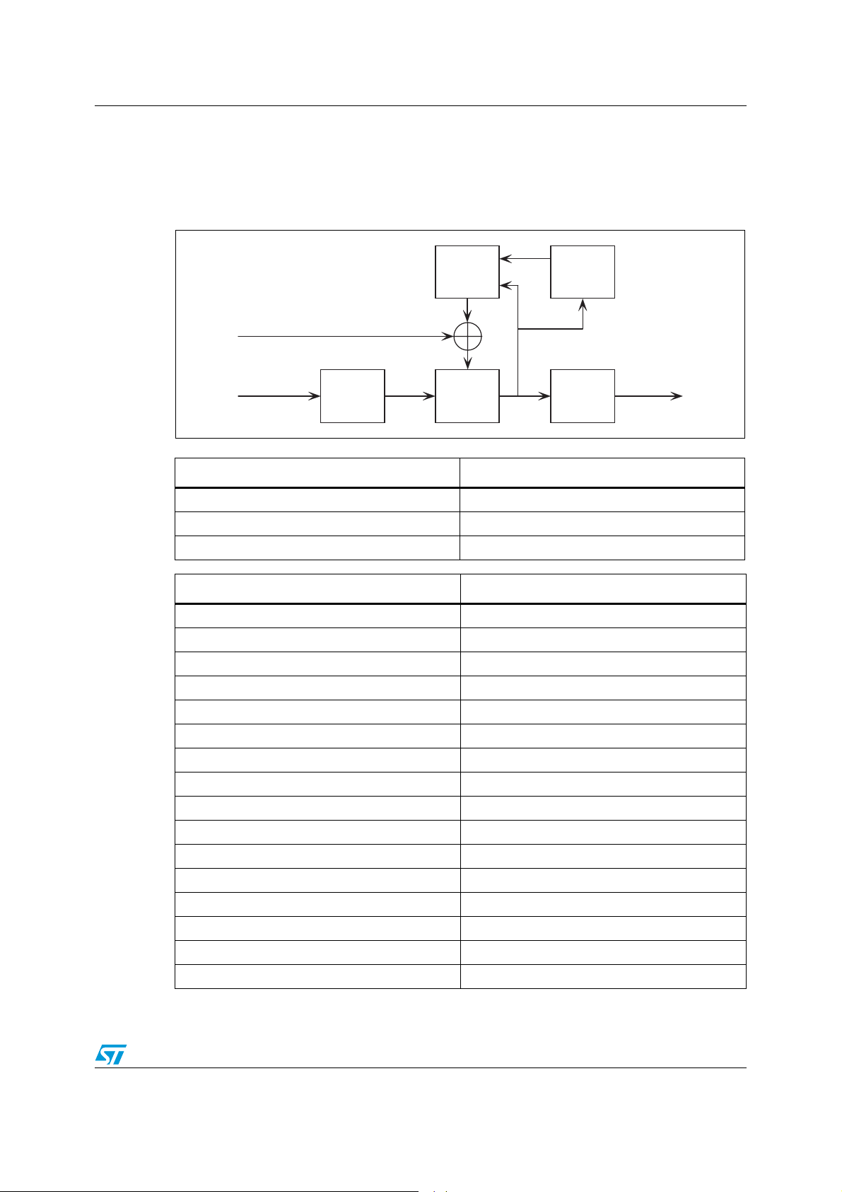
STA309B Registers
In AC mode the attack and release thresholds are set relative to full-scale. In DRC mode the
attack threshold is set relative to the maximum volume setting of the channels mapped to
that limiter and the release threshold is set relative to the maximum volume setting, plus the
attack threshold.
Figure 7. Basic limiter and volume flow diagram
RMSLimiter
Gain/Volume
tuptuOtupnI
Gain
CnLS[1,0] Channel limiter mapping
00 Channel has limiting disabled
01 Channel is mapped to limiter #1
10 Channel is mapped to limiter #2
LnA[3:0] Attack rate (dB/ms)
Attenuation
Saturation
0000 3.1584 (fast)
0001 2.7072
0010 2.2560
0011 1.8048
0100 1.3536
0101 0.9024
0110 0.4512
0111 0.2256
1000 0.1504
1001 0.1123
1010 0.0902
1011 0.0752
1100 0.0645
1101 0.0564
1110 0.0501
1111 0.0451 (slow)
Doc ID 022570 Rev 2 47/66
Page 48
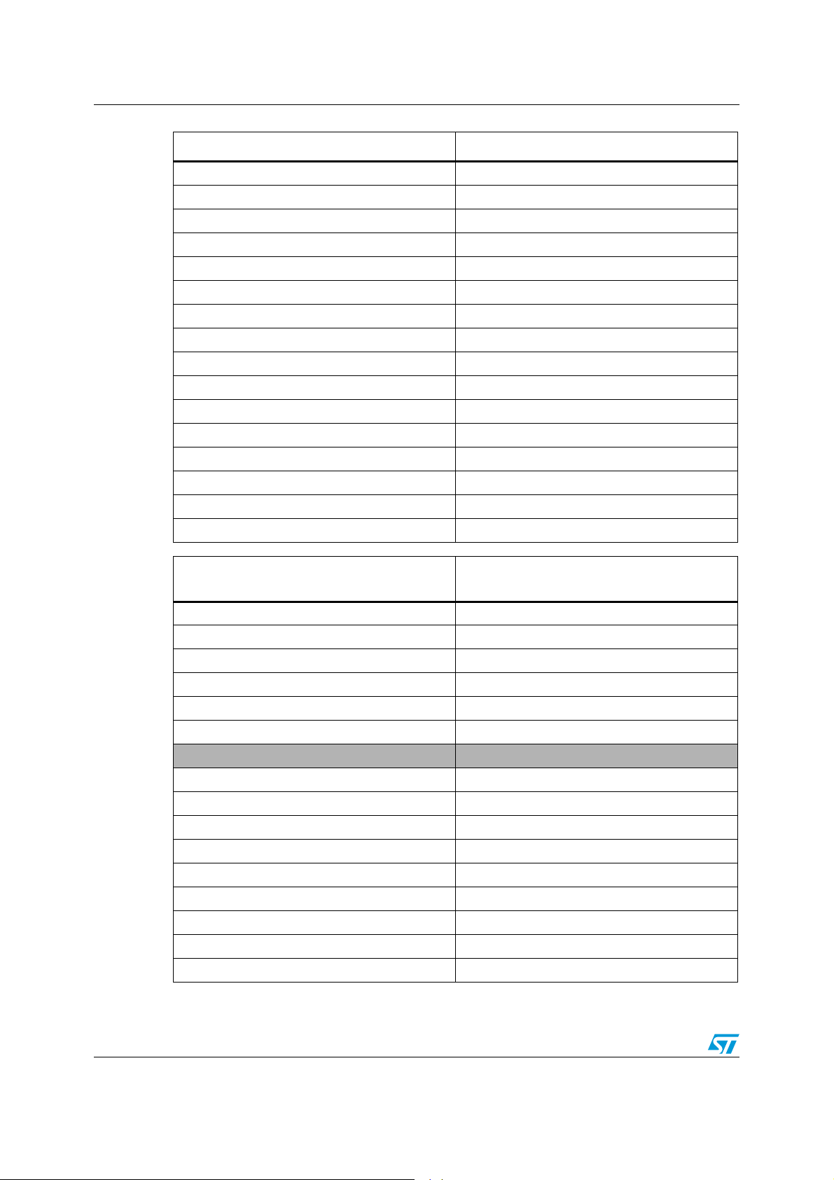
Registers STA309B
LnR[3:0] Release rate (dB/ms)
0000 0.5116 (fast)
0001 0.1370
0010 0.0744
0011 0.0499
0100 0.0360
0101 0.0299
0110 0.0264
0111 0.0208
1000 0.0198
1001 0.0172
1010 0.0147
1011 0.0137
1100 0.0134
1101 0.0117
1110 0.0110
1111 0.0104 (slow)
LnAT[3:0]
0000 -12
0001 -10
0010 -8
0011 -6
0100 -4
0101 -2
0110 0
0111 +2
1000 +3
1001 +4
1010 +5
1011 +6
1100 +7
1101 +8
Anti-clipping (AC)
(dB relative to F
)
S
1110 +9
1111 +10
48/66 Doc ID 022570 Rev 2
Page 49
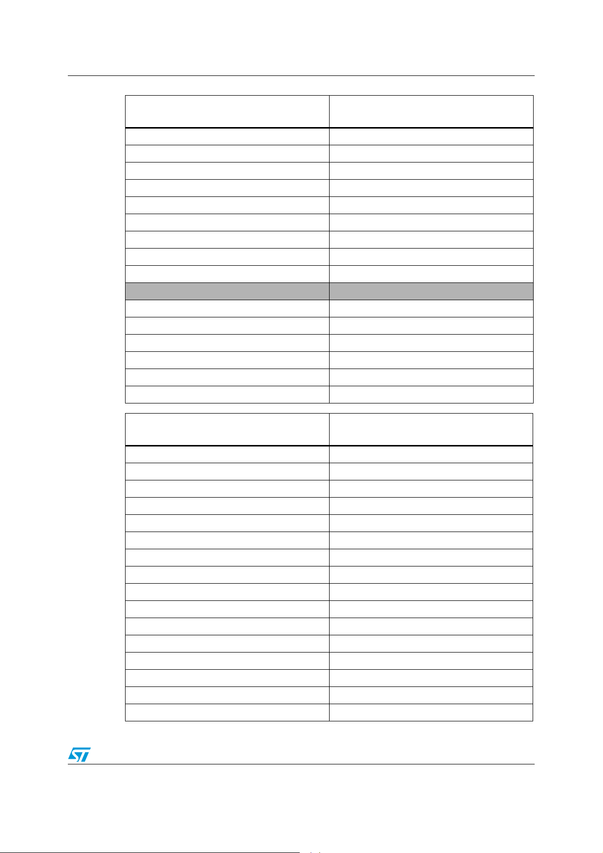
STA309B Registers
LnRT[3:0]
0000 -∞
0001 -29 dB
0010 -20 dB
0011 -16 dB
0100 -14 dB
0101 -12 dB
0110 -10 dB
0111 -8 dB
1000 -7 dB
1001 -6 dB
1010 -5 dB
1011 -4 dB
1100 -3 dB
1101 -2 dB
Anti-clipping (AC)
(dB relative to F
)
S
1110 -1 dB
1111 -0 dB
LnAT[3:0]
0000 -31
0001 -29
0010 -27
0011 -25
0100 -23
0101 -21
0110 -19
0111 -17
1000 -16
1001 -15
1010 -14
1011 -13
1100 -12
Dynamic range compression (DRC)
(dB relative to volume)
1101 -10
1110 -7
1111 -4
Doc ID 022570 Rev 2 49/66
Page 50
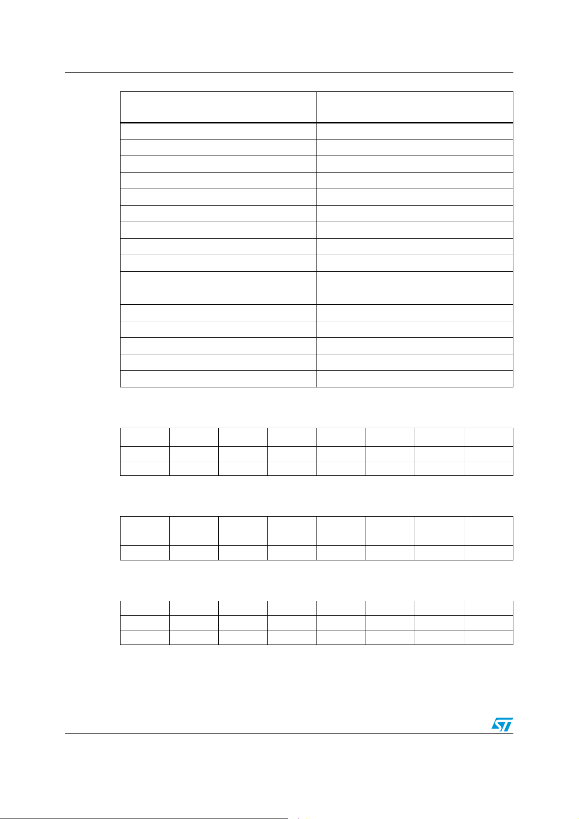
Registers STA309B
LnRT[3:0]
0000 -∞
0001 -38 dB
0010 -36 dB
0011 -33 dB
0100 -31 dB
0101 -30 dB
0110 -28 dB
0111 -26 dB
1000 -24 dB
1001 -22 dB
1010 -20 dB
1011 -18 dB
1100 -15 dB
1101 -12 dB
Dynamic range compression (DRC)
(db relative to volume + LnAT)
1110 -9 dB
1111 -6 dB
7.2.53 Channel 1 and 2 output timing (0x33)
D7 D6 D5 D4 D3 D2 D1 D0
C2OT2 C2OT1 C2OT0 C1OT2 C1OT1 C1OT0
100 000
7.2.54 Channel 3 and 4 output timing (0x34)
D7 D6 D5 D4 D3 D2 D1 D0
C4OT2 C4OT1 C4OT0 C3OT2 C3OT1 C3OT0
110 010
7.2.55 Channel 5 and 6 output timing (0x35)
D7 D6 D5 D4 D3 D2 D1 D0
C6OT2 C6OT1 C6OT0 C5OT2 C5OT1 C5OT0
101 001
50/66 Doc ID 022570 Rev 2
Page 51
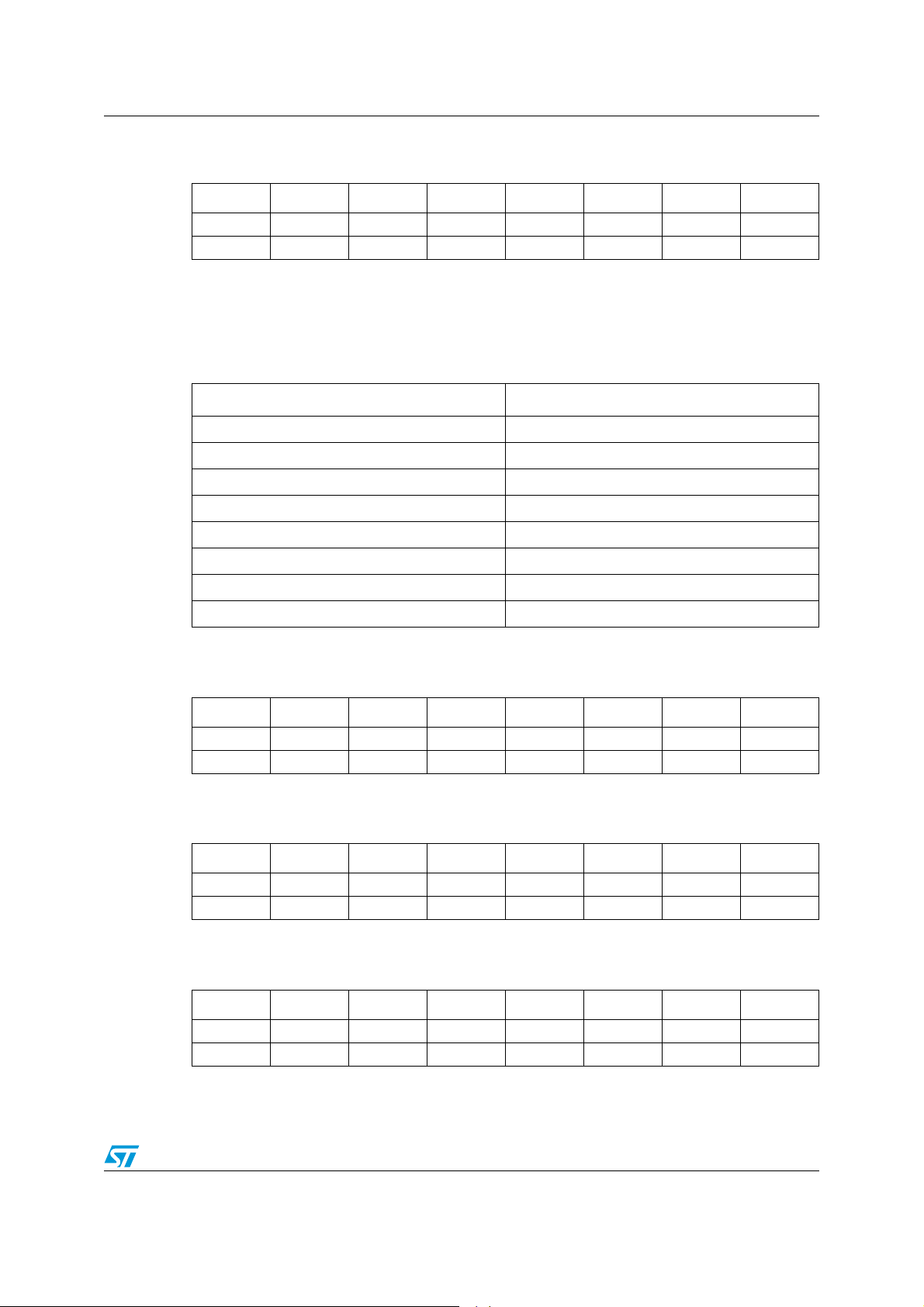
STA309B Registers
7.2.56 Channel 7 and 8 output timing (0x36)
D7 D6 D5 D4 D3 D2 D1 D0
C8OT2 C8OT1 C8OT0 C7OT2 C7OT1 C7OT0
111 011
The centering of the individual channel PWM output periods can be adjusted by the output
timing registers. The PWM slot settings can be chosen to ensure that pulse transitions do
not occur at the same time on different channels using the same power device. There are 8
possible settings, the appropriate setting is based on the application and connections to the
FFX power devices.
CnOT[2:0] PWM slot
000 1
001 2
010 3
011 4
100 5
101 6
110 7
111 8
7.2.57 Channel I2S output mapping channels 1 and 2 (0x37)
D7 D6 D5 D4 D3 D2 D1 D0
C2OM2 C2OM1 C2OM0 C1OM2 C1OM1 C1OM0
001 000
7.2.58 Channel I2S output mapping channels 3 and 4 (0x38)
D7 D6 D5 D4 D3 D2 D1 D0
C4OM2 C4OM1 C4OM0 C3OM2 C3OM1 C3OM0
011 010
7.2.59 Channel I2S output mapping channels 5 and 6 (0x39)
D7 D6 D5 D4 D3 D2 D1 D0
C6OM2 C6OM1 C6OM0 C5OM2 C5OM1 C5OM0
101 100
Doc ID 022570 Rev 2 51/66
Page 52
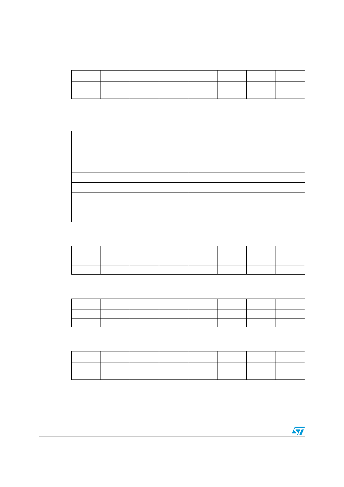
Registers STA309B
7.2.60 Channel I2S output mapping channels 7 and 8 (0x3A)
D7 D6 D5 D4 D3 D2 D1 D0
C8OM2 C8M1 C8OM0 C7OM2 C7OM1 C7OM0
111 110
Each I2S output channel can receive data from any channel output of the volume block.
Which channel a particular I
2
S output receives is dependent upon that channel’s CnOM
register bits.
CnOM[2:0] Serial output from
000 Channel 1
001 Channel 2
010 Channel 3
011 Channel 4
100 Channel 5
101 Channel 6
110 Channel 7
111 Channel 8
7.2.61 Coefficient address register 1 (0x3B)
D7 D6 D5 D4 D3 D2 D1 D0
CFA9 CFA8
00
7.2.62 Coefficient address register 2 (0x3C)
D7 D6 D5 D4 D3 D2 D1 D0
CFA7 CFA6 CFA5 CFA4 CFA3 CFA2 CFA1 CFA0
00000000
7.2.63 Coefficient b1 data register, bits 23:16 (0x3D)
D7 D6 D5 D4 D3 D2 D1 D0
C1B23 C1B22 C1B21 C1B20 C1B19 C1B18 C1B17 C1B16
00000000
52/66 Doc ID 022570 Rev 2
Page 53
STA309B Registers
7.2.64 Coefficient b1 data register, bits 15:8 (0x3E)
D7 D6 D5 D4 D3 D2 D1 D0
C1B15 C1B14 C1B13 C1B12 C1B11 C1B10 C1B9 C1B8
00000000
7.2.65 Coefficient b1 data register, bits 7:0 (0x3F)
D7 D6 D5 D4 D3 D2 D1 D0
C1B7 C1B6 C1B5 C1B4 C1B3 C1B2 C1B1 C1B0
00000000
7.2.66 Coefficient b2 data register, bits 23:16 (0x40)
D7 D6 D5 D4 D3 D2 D1 D0
C2B23 C2B22 C2B21 C2B20 C2B19 C2B18 C2B17 C2B16
00000000
7.2.67 Coefficient b2 data register, bits 15:8 (0x41)
D7 D6 D5 D4 D3 D2 D1 D0
C2B15 C2B14 C2B13 C2B12 C2B11 C2B10 C2B9 C2B8
00000000
7.2.68 Coefficient b2 data register, bits 7:0 (0x42)
D7 D6 D5 D4 D3 D2 D1 D0
C2B7 C2B6 C2B5 C2B4 C2B3 C2B2 C2B1 C2B0
00000000
7.2.69 Coefficient a1 data register, bits 23:16 (0x43)
D7 D6 D5 D4 D3 D2 D1 D0
C1B23 C1B22 C1B21 C1B20 C1B19 C1B18 C1B17 C1B16
00000000
7.2.70 Coefficient a1 data register, bits 15:8 (0x44)
D7 D6 D5 D4 D3 D2 D1 D0
C3B15 C3B14 C3B13 C3B12 C3B11 C3B10 C3B9 C3B8
00000000
Doc ID 022570 Rev 2 53/66
Page 54
Registers STA309B
7.2.71 Coefficient a1 data register, bits 7:0 (0x45)
D7 D6 D5 D4 D3 D2 D1 D0
C3B7 C3B6 C3B5 C3B4 C3B3 C3B2 C3B1 C3B0
00000000
7.2.72 Coefficient a2 data register, bits 23:16 (0x46)
D7 D6 D5 D4 D3 D2 D1 D0
C4B23 C4B22 C4B21 C4B20 C4B19 C4B18 C4B17 C4B16
00000000
7.2.73 Coefficient a2 data register, bits 15:8 (0x47)
D7 D6 D5 D4 D3 D2 D1 D0
C4B15 C4B14 C4B13 C4B12 C4B11 C4B10 C4B9 C4B8
00000000
7.2.74 Coefficient a2 data register, bits 7:0 (0x48)
D7 D6 D5 D4 D3 D2 D1 D0
C4B7 C4B6 C4B5 C4B4 C4B3 C4B2 C4B1 C4B0
00000000
7.2.75 Coefficient b0 data register, bits 23:16 (0x49)
D7 D6 D5 D4 D3 D2 D1 D0
C5B23 C5B22 C5B21 C5B20 C5B19 C5B18 C5B17 C5B16
00000000
7.2.76 Coefficient b0 data register, bits 15:8 (0x4A)
D7 D6 D5 D4 D3 D2 D1 D0
C5B15 C5B14 C5B13 C5B12 C5B11 C5B10 C5B9 C5B8
00000000
7.2.77 Coefficient b0 data register, bits 7:0 (0x4B)
D7 D6 D5 D4 D3 D2 D1 D0
C5B7 C5B6 C5B5 C5B4 C5B3 C5B2 C5B1 C5B0
00000000
54/66 Doc ID 022570 Rev 2
Page 55

STA309B Registers
7.2.78 Coefficient write control register (0x4C)
D7 D6 D5 D4 D3 D2 D1 D0
WA W1
00
Coefficients for EQ and bass management are handled internally in the STA309B via RAM.
Access to this RAM is available to the user via an I
A collection of I
2
C registers are dedicated to this function. One contains a coefficient base
2
C register interface.
address, five sets of three store the values of the 24-bit coefficients to be written or that were
read, and one contains bits used to control the write of the coefficient(s) to RAM. The
following are instructions for reading and writing coefficients.
7.3 Reading a coefficient from RAM
1. write top 2 bits of address to I2C register 0x3B
2. write bottom 8 bits of address to I
3. read top 8 bits of coefficient in I
4. read middle 8 bits of coefficient in I
5. read bottom 8 bits of coefficient in I
2
C register 0x3C
2
C address 0x3D
2
C address 0x3E
2
C address 0x3F
7.4 Reading a set of coefficients from RAM
1. write top 2 bits of address to I2C register 0x3B
2. write bottom 8 bits of address to I
3. read top 8 bits of coefficient in I
4. read middle 8 bits of coefficient in I
5. read bottom 8 bits of coefficient in I
6. read top 8 bits of coefficient b2 in I
7. read middle 8 bits of coefficient b2 in I
8. read bottom 8 bits of coefficient b2 in I
9. read top 8 bits of coefficient a1 in I
10. read middle 8 bits of coefficient a1 in I
11. read bottom 8 bits of coefficient a1 in I
12. read top 8 bits of coefficient a2 in I
13. read middle 8 bits of coefficient a2 in I
14. read bottom 8 bits of coefficient a2 in I
15. read top 8 bits of coefficient b0 in I
16. read middle 8 bits of coefficient b0 in I
17. read bottom 8 bits of coefficient b0 in I
2
C register 0x3C
2
C address 0x3D
2
C address 0x3E
2
C address 0x3F
2
C address 0x40
2
C address 0x41
2
C address 0x42
2
C address 0x43
2
C address 0x44
2
C address 0x45
2
C address 0x46
2
C address 0x47
2
C address 0x48
2
C address 0x49
2
C address 0x4A
2
C address 0x4B
Doc ID 022570 Rev 2 55/66
Page 56

Registers STA309B
7.5 Writing a single coefficient to RAM
1. write top 2 bits of address to I2C register 0x3B
2. write bottom 8 bits of address to I
3. write top 8 bits of coefficient in I
4. write middle 8 bits of coefficient in I
5. write bottom 8 bits of coefficient in I
6. write 1 to W1 bit in I
2
C address 0x4C
2
C register 0x3C
2
C address 0x3D
2
C address 0x3E
2
C address 0x3F
7.6 Writing a set of coefficients to RAM
1. write top 2 bits of starting address to I2C register 0x3B
2. write bottom 8 bits of starting address to I
3. write top 8 bits of coefficient b1 in I
4. write middle 8 bits of coefficient b1 in I
5. write bottom 8 bits of coefficient b1 in I
6. write top 8 bits of coefficient b2 in I
7. write middle 8 bits of coefficient b2 in I
8. write bottom 8 bits of coefficient b2 in I
9. write top 8 bits of coefficient a1 in I
10. write middle 8 bits of coefficient a1 in I
11. write bottom 8 bits of coefficient a1 in I
12. write top 8 bits of coefficient a2 in I
13. write middle 8 bits of coefficient a2 in I
14. write bottom 8 bits of coefficient a2 in I
15. write top 8 bits of coefficient b0 in I
16. write middle 8 bits of coefficient b0 in I
17. write bottom 8 bits of coefficient b0 in I
18. write 1 to WA bit in I
2
C address 0x4C
2
C register 0x3C
2
C address 0x3D
2
C address 0x3E
2
C address 0x3F
2
C address 0x40
2
C address 0x41
2
C address 0x42
2
C address 0x43
2
C address 0x44
2
C address 0x45
2
C address 0x46
2
C address 0x47
2
C address 0x48
2
C address 0x49
2
C address 0x4A
2
C address 0x4B
The mechanism for writing a set of coefficients to RAM provides a method of updating the
five coefficients corresponding to a given biquad (filter) simultaneously to avoid possible
unpleasant acoustic side-effects.
When using this technique, the 10-bit address specifies the address of the biquad b1
coefficient (for example, decimals 0, 5, 10, 15, …, 100, … 395), and the STA309B generates
the RAM addresses as offsets from this base value to write the complete set of coefficient
data.
56/66 Doc ID 022570 Rev 2
Page 57
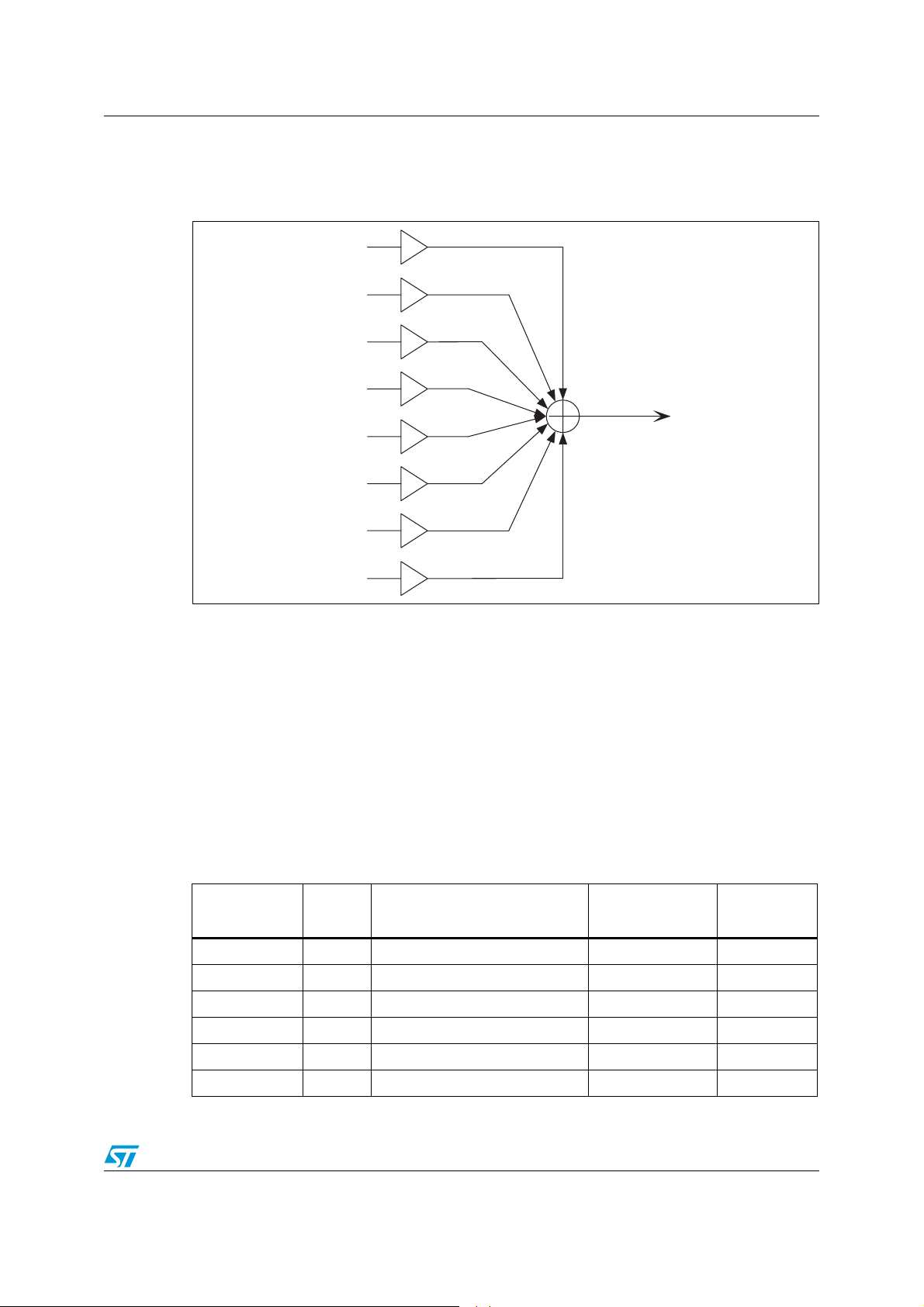
STA309B Equalization and mixing
8 Equalization and mixing
Figure 8. Channel mixer
CxMIX1
Channel 1
CxMIX2
Channel 2
CxMIX3
Channel 3
8.1 Post-scale
The STA309B provides one additional multiplication after the last interpolation stage and
before the distortion compensation on each channel. This is a 24-bit signed fractional
multiplier.
The scale factor for this multiplier is loaded into RAM using the same I
biquad coefficients and the bass-management.
This post-scale factor can be used in conjunction with an ADC-equipped microcontroller to
perform power-supply error correction. All channels can use channel 1 by setting the postscale link bit.
Table 9. RAM block for biquads, mixing, and bass management
Channel 4
Channel 5
Channel 6
Channel 7
Channel 8
CxMIX4
CxMIX5
CxMIX6
CxMIX7
CxMIX8
Channel x
2
C registers as the
Index
(decimal)
Index
(hex)
Coefficient Default
0 0x00 Channel 1 - Biquad 1 C1H10 (b1/2) 0x000000
1 0x01 C1H11 (b2) 0x000000
2 0x02 C1H12 (a1/2) 0x000000
3 0x03 C1H13 (a2) 0x000000
4 0x04 C1H14 (b0/2) 0x400000
5 0x05 Channel 1 - Biquad 2 C1H20 0x000000
Doc ID 022570 Rev 2 57/66
Page 58
Equalization and mixing STA309B
Table 9. RAM block for biquads, mixing, and bass management (continued)
Index
(decimal)
……… … …
49 0x31 Channel 1 - Biquad 10 C1HA4 0x400000
50 0x32 Channel 2 - Biquad 1 C2H10 0x000000
51 0x33 C2H11 0x000000
……… … …
99 0x63 Channel 2 - Biquad 10 C2HA4 0x4000000
100 0x64 Channel 3 - Biquad 1 C3H10 0x000000
……… … …
399 0x18F Channel 8 - Biquad 10 C8HA4 0x400000
400 0x190 Channel 1 - Pre-Scale C1PreS 0x7FFFFF
401 0x191 Channel 2 - Pre-Scale C2PreS 0x7FFFFF
402 0x192 Channel 3 - Pre-Scale C3PreS 0x7FFFFF
……… … …
407 0x197 Channel 8 - Pre-Scale C8PreS 0x7FFFFF
408 0x198 Channel 1 - Post-Scale C1PstS 0x7FFFFF
409 0x199 Channel 2 - Post-Scale C2PstS 0x7FFFFF
……… … …
Index
(hex)
Coefficient Default
415 0x19F Channel 8 - Post-Scale C8PstS 0x7FFFFF
416 0x1A0 Channel 1 - Mix#1 1 C1MX11 0x7FFFFF
417 0x1A1 Channel 1 - Mix#1 2 C1MX12 0x000000
……… … …
423 0x1A7 Channel 1 - Mix#1 8 C1MX18 0x000000
424 0x1A8 Channel 2 - Mix#1 1 C2MX11 0x000000
425 0x1A9 Channel 2 - Mix#1 2 C2MX12 0x7FFFFF
……… … …
463 0x1CF Channel 8 - Mix#1 8 C8MX18 0x7FFFFF
464 0x1D0 Channel 1 - Mix#2 1 C1MX21 0x7FFFFF
465 0x1D1 Channel 1 - Mix#2 2 C1MX22 0x000000
……… … …
471 0x1D7 Channel 1 - Mix#2 8 C1MX28 0x000000
472 0x1D8 Channel 2 - Mix#2 1 C2MX21 0x000000
473 0x1D9 Channel 2 - Mix#2 2 C2MX22 0x7FFFFF
……… … …
527 0x20F Channel 8 - Mix#2 8 C8MX28 0x7FFFFF
58/66 Doc ID 022570 Rev 2
Page 59
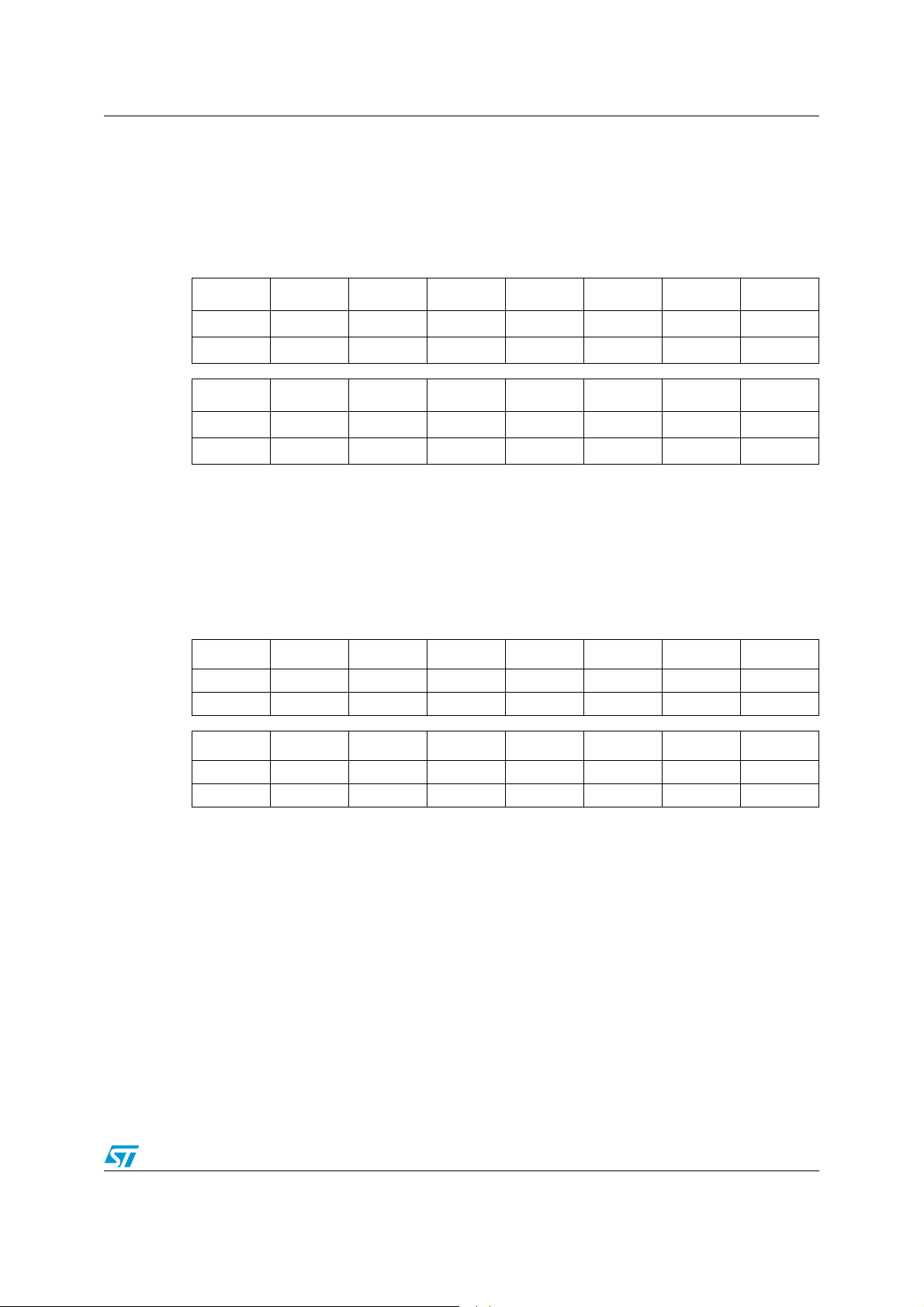
STA309B Equalization and mixing
8.2 Variable maximum power correction
8.2.1 MPCC1-2 (0x4D, 0x4E)
The MPCC bits determine the 16 MSBs of the MPC compensation coefficient. This
coefficient is used in place of the default coefficient when MPCV = 1.
D7 D6 D5 D4 D3 D2 D1 D0
MPCC15 MPCC14 MPCC13 MPCC12 MPCC11 MPCC10 MPCC9 MPCC8
00101101
D7 D6 D5 D4 D3 D2 D1 D0
MPCC7 MPCC6 MPCC5 MPCC4 MPCC3 MPCC2 MPCC1 MPCC0
11000000
8.3 Variable distortion compensation
8.3.1 DCC1-2 (0x4F, 0x50)
The DCC bits determine the 16 MSBs of the distortion compensation coefficient. This
coefficient is used in place of the default coefficient when DCCV = 1.
D7 D6 D5 D4 D3 D2 D1 D0
DCC15 DCC14 DCC13 DCC12 DCC11 DCC10 DCC9 DCC8
11110011
D7 D6 D5 D4 D3 D2 D1 D0
DCC7 DCC6 DCC5 DCC4 DCC3 DCC2 DCC1 DCC0
00110011
Doc ID 022570 Rev 2 59/66
Page 60
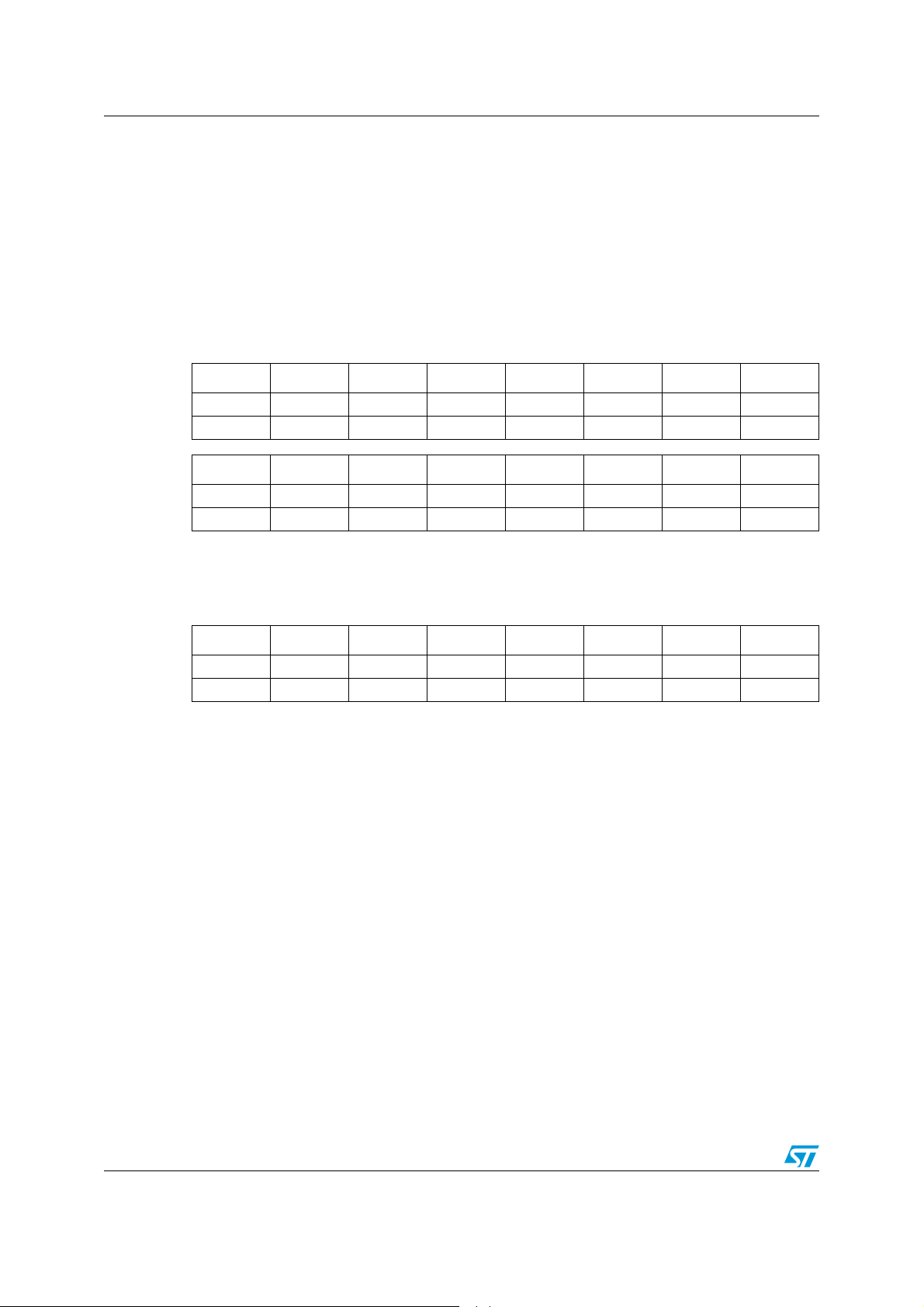
Equalization and mixing STA309B
8.4 PSCorrect registers
ADC is used to input ripple data to SDI78. The left channel (7) is used internally. No audio
data can therefore be used on these channels, although all channel mapping and mixing
from other inputs to channels 7 and 8 internally are still valid.
8.4.1 PSC1-2: ripple correction value (RCV) (0x51, 0x52)
This function is equivalent to the negative maximum ripple peak as a percentage of Vcc
(MPR), scaled by the inverse of the maximum ripple p-p as a percentage of full-scale analog
input to ADC. It is represented as a 1.11 signed fractional number.
D7 D6 D5 D4 D3 D2 D1 D0
RCV11 RCV10 RCV9 RCV8 RCV7 RCV6 RCV5 RCV4
00000000
D7 D6 D5 D4 D3 D2 D1 D0
RCV3 RCV2 RCV1 RCV0 CNV11 CNV10 CNV9 CNV8
00001111
8.4.2 PSC3: correction normalization value (CNV) (0x53)
This function is equivalent to 1 / (1+MPR) expressed as a 0.12 unsigned fractional number.
D7 D6 D5 D4 D3 D2 D1 D0
CNV7 CNV6 CNV5 CNV4 CNV3 CNV2 CNV1 CNV0
11111111
8.5 Digital pop-free operation in single-ended mode
The STA309B pop-free feature allows digitally pre-loading the bypass capacitor between the
filtered amplifier output and the load in single-ended applications. Normally, a bypass
capacitor needs to be preloaded to half of the power supply in order to avoid having popnoise at PWM startup.
By enabling the STA309B pop-free feature, it is possible to preload the capacitor using the
amplifier, without needing the resistive partition. By forcing a ramp, it is possible to gradually
load the capacitor from zero to half the supply with the PWM signal starting from near 0%
duty cycle to 50% duty cycle. This “active load” is also faster than the resistive partition
method.
60/66 Doc ID 022570 Rev 2
Page 61
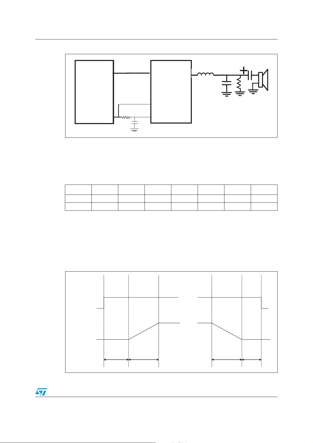
STA309B Equalization and mixing
Figure 9. Typical single-ended driver - power stage configuration
Cbyp
Cbyp
Cbyp
yxTUOyxTUO
yxTUOyxTUO
INxy
INxy
INxy
STA5xx
STA5xx
STA309B
STA309B
STA309B
EAPD
EAPD
EAPD
The R pull-down resistor (typical value: 3.3 kOhm) is placed to ensure that there is zero
voltage across the load and the bypass capacitor is discharged when the amplifier is in
tristate mode.
STA5xx
PWRDN
PWRDN
PWRDN
TRI-STATE
TRI-STATE
TRI-STATE
yxTUOyxTUO
8.5.1 PFCXON: digital pop-free register (0x5F)
D7 D6 D5 D4 D3 D2 D1 D0
CH8 CH7 CH6 CH5 CH4 CH3 CH2 CH1
11111111
PFCXON[I]:
when ‘1’, digital pop free is active on channel i+1 when in binary mode (see
Section 7.2.5: Configuration register E (0x04) on page 28)
when ‘0’, digital pop free is not active on channel i+1
8.5.2 Timing settings
Figure 10. Pop-free timing diagram
EAPD
EAPD
OUT
OUT
GND
GND
VCC/2
VCC/2
…
…
TSPUPT
TSPUPT
RAMPTIM
RAMPTIM
RAMPTIM
Doc ID 022570 Rev 2 61/66
RAMPTIM
LSPDWT
LSPDWT
Page 62
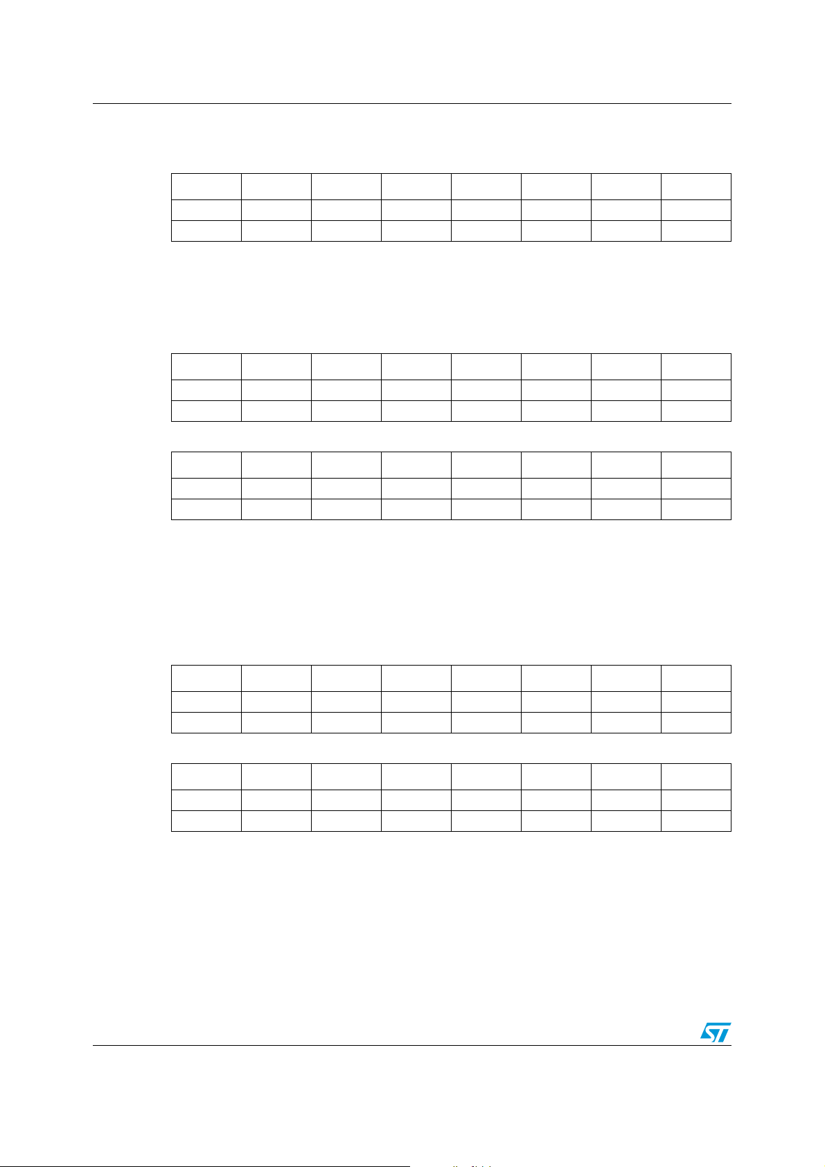
Equalization and mixing STA309B
8.5.3 RAMPTIM: ramp duration register (0x66)
D7 D6 D5 D4 D3 D2 D1 D0
TR7 TR6 TR5 TR4 TR3 TR2 TR1 TR0
00000100
This function is the total pop-free ramp duration (same value for ramp-up and ramp-down
and for all channels); default is 400 ms (range is 0-25 sec.).
8.5.4 TSPUPT: waiting time after EAPD (0x67 - 0x68)
D7 D6 D5 D4 D3 D2 D1 D0
TP15 TP14 TP13 TP12 TP11 TP10 TP9 TP8
00010000
D7 D6 D5 D4 D3 D2 D1 D0
TP7 TP6 TP5 TP4 TP3 TP2 TP1 TP0
00000000
This function is the waiting time after EAPD=1 to start ramp-up (same value for all
channels); default is 680 ms (range is 0-11 sec.). In a typical application the EAPD line is
connected to the TRI-STATE input pin of the STA5xx power stage through the RC filter (see
Figure 9 on page 61). TSPUPT shall be greater than the RC time constant.
8.5.5 LSPDWT: waiting time before EAPD (0x71 - 0x72)
D7 D6 D5 D4 D3 D2 D1 D0
TL15 TL14 TLP13 TL12 TL11 TL10 TL9 TL8
00100000
D7 D6 D5 D4 D3 D2 D1 D0
TL7 TL6 TL5 TL4 TL3 TL2 TL1 TL0
00000000
This function is the waiting time after end of ramp-down to assert EAPD=0 (same value for
all channels); default is 1.4 sec. (range is 0-11 sec.). If a resistor is placed in parallel to the
output filter capacitor (see Figure 9 on page 61), the LSPDWT value is 0x00.
62/66 Doc ID 022570 Rev 2
Page 63
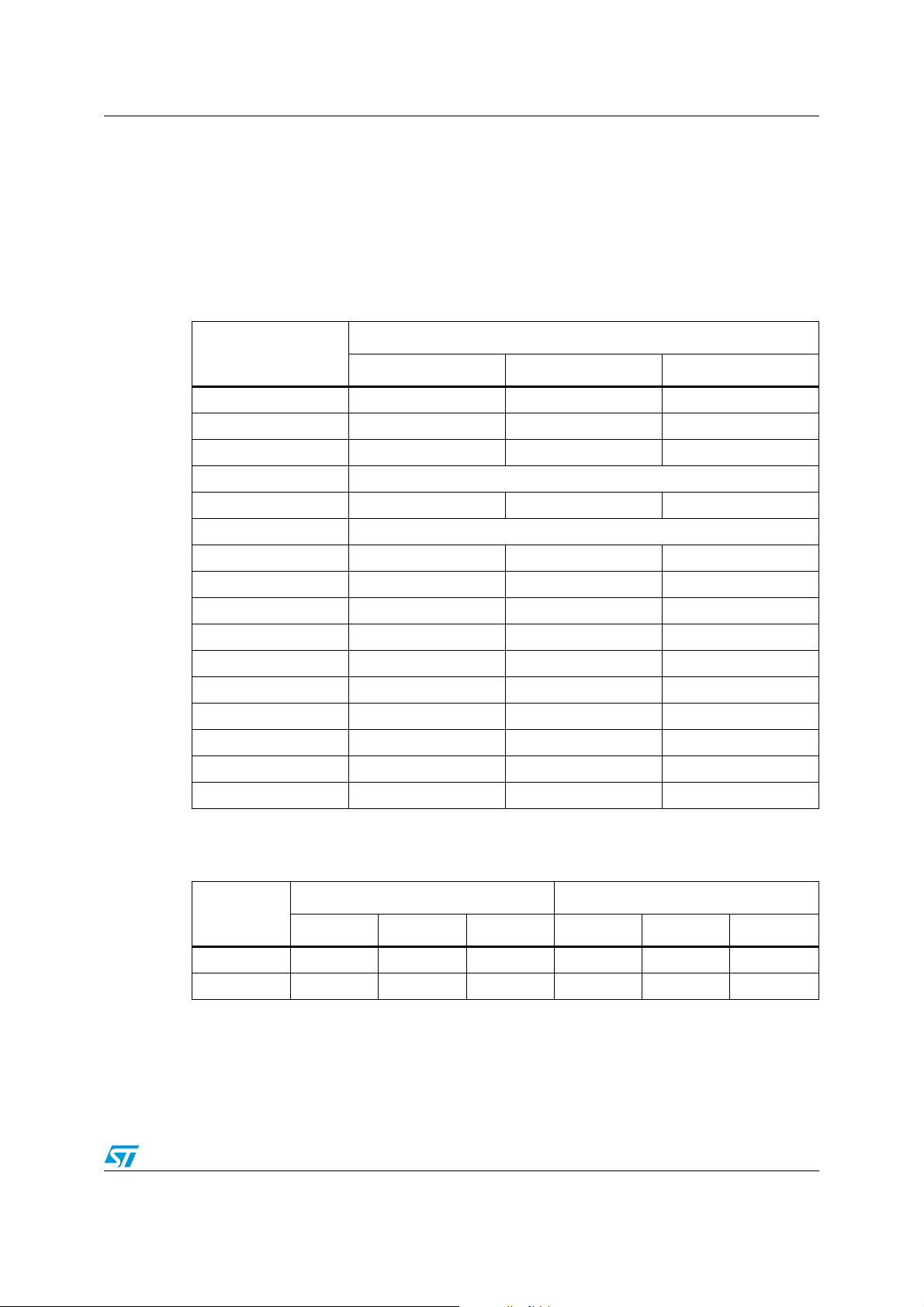
STA309B Package information
9 Package information
In order to meet environmental requirements, ST offers these devices in different grades of
ECOPACK
specifications, grade definitions and product status are available at: www.st.com.
ECOPACK
®
packages, depending on their level of environmental compliance. ECOPACK®
®
is an ST trademark.
Table 10. VFQFPN-56 (8 x 8 mm) package dimensions
mm
Reference
Min. Typ. Max.
A 0.80 0.90 1.00
A1 0 0.05
D8.00
D2 See exposed pad variations
E8.00
E2 See exposed pad variations
b 0.25 0.30 0.35
b1 0.20 0.25 0.30
e (pad pitch)
(1)
L1 0.05 0.15
aaa 0.15
bbb 0.10
ddd 0.05
eee 0.08
fff 0.10
ccc 0.10
1. Refer to Figure 11.
Table 11. Exposed pad variations
D2 E2
Variati on
Min. Typ. Max Min. Typ. Max.
A 5.85 5.90 5.95 5.85 5.90 5.95
B 4.25 4.30 4.35 4.25 4.30 4.35
Doc ID 022570 Rev 2 63/66
Page 64
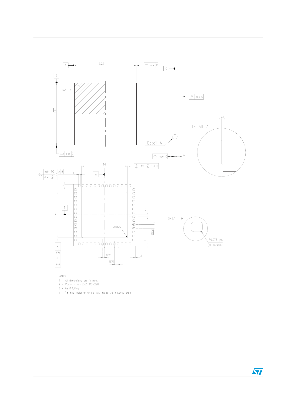
Package information STA309B
Figure 11. VFQFPN-56 (8 x 8 mm) package outline
The axis of each pad must lie simultaneously in both tolerance zones.
(4) - The terminal A1 corner must be identified on the top surface through inked or lasered mark dot.
A distinguishing feature is allowable on the bottom surface of the package, chamfer at die paddle corner to
identify the terminal A1. Exact shape of each corner is optional.
(5) – All dimensions are in mm.
64/66 Doc ID 022570 Rev 2
826820
Page 65

STA309B Revision history
10 Revision history
Table 12. Document revision history
Date Revision Changes
09-Dec-2011 1 Initial release
24-Jan-2012 2 Updated title and Description on page 1
Doc ID 022570 Rev 2 65/66
Page 66

STA309B
Please Read Carefully:
Information in this document is provided solely in connection with ST products. STMicroelectronics NV and its subsidiaries (“ST”) reserve the
right to make changes, corrections, modifications or improvements, to this document, and the products and services described herein at any
time, without notice.
All ST products are sold pursuant to ST’s terms and conditions of sale.
Purchasers are solely responsible for the choice, selection and use of the ST products and services described herein, and ST assumes no
liability whatsoever relating to the choice, selection or use of the ST products and services described herein.
No license, express or implied, by estoppel or otherwise, to any intellectual property rights is granted under this document. If any part of this
document refers to any third party products or services it shall not be deemed a license grant by ST for the use of such third party products
or services, or any intellectual property contained therein or considered as a warranty covering the use in any manner whatsoever of such
third party products or services or any intellectual property contained therein.
UNLESS OTHERWISE SET FORTH IN ST’S TERMS AND CONDITIONS OF SALE ST DISCLAIMS ANY EXPRESS OR IMPLIED
WARRANTY WITH RESPECT TO THE USE AND/OR SALE OF ST PRODUCTS INCLUDING WITHOUT LIMITATION IMPLIED
WARRANTIES OF MERCHANTABILITY, FITNESS FOR A PARTICULAR PURPOSE (AND THEIR EQUIVALENTS UNDER THE LAWS
OF ANY JURISDICTION), OR INFRINGEMENT OF ANY PATENT, COPYRIGHT OR OTHER INTELLECTUAL PROPERTY RIGHT.
UNLESS EXPRESSLY APPROVED IN WRITING BY TWO AUTHORIZED ST REPRESENTATIVES, ST PRODUCTS ARE NOT
RECOMMENDED, AUTHORIZED OR WARRANTED FOR USE IN MILITARY, AIR CRAFT, SPACE, LIFE SAVING, OR LIFE SUSTAINING
APPLICATIONS, NOR IN PRODUCTS OR SYSTEMS WHERE FAILURE OR MALFUNCTION MAY RESULT IN PERSONAL INJURY,
DEATH, OR SEVERE PROPERTY OR ENVIRONMENTAL DAMAGE. ST PRODUCTS WHICH ARE NOT SPECIFIED AS "AUTOMOTIVE
GRADE" MAY ONLY BE USED IN AUTOMOTIVE APPLICATIONS AT USER’S OWN RISK.
Resale of ST products with provisions different from the statements and/or technical features set forth in this document shall immediately void
any warranty granted by ST for the ST product or service described herein and shall not create or extend in any manner whatsoever, any
liability of ST.
ST and the ST logo are trademarks or registered trademarks of ST in various countries.
Information in this document supersedes and replaces all information previously supplied.
The ST logo is a registered trademark of STMicroelectronics. All other names are the property of their respective owners.
© 2012 STMicroelectronics - All rights reserved
STMicroelectronics group of companies
Australia - Belgium - Brazil - Canada - China - Czech Republic - Finland - France - Germany - Hong Kong - India - Israel - Italy - Japan -
Malaysia - Malta - Morocco - Philippines - Singapore - Spain - Sweden - Switzerland - United Kingdom - United States of America
www.st.com
66/66 Doc ID 022570 Rev 2
 Loading...