

Page 1

STA308
MULTICHANNEL DIGITAL AUDIO PROCESSOR WITH DDX™
PRODUCT PREVIEW
■ 8 DDX
■ From 32kHz to 192kHz Input Sample Rates
■ Volume Control from 0 to -100dB (0.5 dB steps)
■ Variable Digital Gain from 0 to 24dB (0.5dB
■ I2S Inputs and Outputs
■ Individual Channel and Master Gain/
■ Individual Channel Mute and Zero Input Detect
■ Selectable Serial Audio Data Interface
■ Bass/T re b le C on t r ols
■ Channel Mapping of any Input to any
■ Active Crossover Capability
■ DC Blocking Selectable High-Pass Filter
■ Selectable Bass Managemen t on Channel 6
■ Selectable Adjacent Channel Mixing Capabili ty
■ Selectable DDX
■ Selectable Clock Input Ratio
■ Selectable De-emphasis
■ Selectable DDX
■ AM Interference Reduction Mode
■ I2C Control
TM
Channels Capability (24 bit)
Supported
steps) with Digital Limiter Functionality and
Variable Attack and Release Time
Attenuation
Auto-Mute
Processing/DDX
TM
Channel
TM
Headphone Output on
Channels 7 & 8
TM
Ternary, or Binary PWM
output
TQFP64
ORDERING NUMBER: STA308
DESCRIPTION
The STA308 is a single chip solution for digital audio
processing and control in multi-channel applications.
It provides output capabilities for DDX
tal Amplification). In conjunction with a DDX
TM
(Direct Digi-
TM
power
device, it provides high-quality, high-efficiency, all
digital amplification. The device is extremely versatile
allowing for input of most digital formats including 6.1
channel and 192kHz, 24-bit DVD-Audio.
The internal 24-bit DSP allows for high resolution
processing at all standard input sample frequencies.
Processing includes volume control, filtering, bass
management, gain compression/limiting and PCM
and DDX
TM
outputs. Filtering includes five user-programmable 28-bit biquads for EQ per channel, as
well as bass, treble and DC blocking. External clocking can be provided at 4 different ratios of the input
sample frequency. All sample frequencies are upsampled for processing. Each internal processing
channel can receive any input channel, allowing flexibility and the ability to perform active digital crossover for powered loudspeaker systems.
The serial audio data i nterface accept s many different formats, includi ng the popular I 2S format. Eight
channels of DDX processing are performed.
December 2002
This is preliminary information on a new product foreseen to be developed. Details are subject to change without notice.
1/33
Page 2

STA308
(
)
BLOCK DIAGRAM
LRCKI
BICKI
SDI12
SDI34
SDI56
SDI78
PLLB
SERIAL
DATA
IN
CHANNEL
MAPPING
SYSTEM TIMING
PLL
XTI
CKOUT
Figure 1. Signal Fl ow Diagram
Channels 1-8
1st Stage
I n terpolation
Output
SA
VARIABLE
OVER-
SAMPLING
Interp_Rate
SCL
SDA
I2C
SYSTEM
CONTROL
POWER
DOWN
PWDN
Scale
& Mix
MVO
OVERSAMPLING
TREBLE,
BASS, EQ
BIQUADS
EAPD
VOLUME
LIMITING
VARIABLE
DOWN-
SAMPLING
Bass Management
(Channel 6 only)
DDX
SERIAL
DATA
OUT
OUT1A/B
OUT2A/B
OUT3A/B
OUT4A/B
OUT5A/B
OUT6A/B
OUT7A/B
OUT8A/B
LRCKO
BICKO
SDO12
SDO34
SDO56
SDO78
8 Inputs
FromI2S
Channel
Mappi ng
1x,2x,4x
BME
Interp
Noise & Distortion Reduction
Biquads
B/T
Volume
Lim iter
(Channels 7&8 only)
PWM
DDX
Headphone
2x
Interp
DDX
Output
2/33
Page 3

STA308
IN CONNECTION
(Top view)
MVO
GND
VDD3
GND
VDD
SDI_78
SDI_56
SDI_34
SDI_12
LRCKI
BICKI
VDD3
GND
VDD
RESET
PLLB
SDO_78
PWDN
63
64
1
2
3
4
5
6
7
8
9
10
12
13
14
15
16
17 18 19 20 21
SA
SDA
SDO_56
62
SCL
GND
VDD
VDD3
SDO_34
SDO_12
LRCKO
VDD
BICKO
60
61
59 58 57 56 5455 53 52 51 50 49
22 23 24 25 26
XTI
VDDA
FILTER_PLL
GNDA
VDD3
VDD
CKOUT
271128 29 30 31 32
GND
GND
VDD3
VDD3
EAPD
OUT8_B
OUT8_A
OUT1_A
OUT1_B
OUT7_B
OUT7_A
48
47
46
45
44
43
42
41
40
39
38
37
36
35
34
33
D02AU1356
OUT2_A
OUT2_B
VDD
GND
VDD3
OUT3_A
OUT3_B
OUT4_A
OUT4_B
OUT5_A
OUT5_B
VDD
GND
VDD3
OUT6_A
OUT6_B
PIN FUNCTION
PIN NAME TYPE DESCRIPTION PAD TYPE
1 MVO I Master Volume Override CMOS Input Buffer with
3, 12, 24, 28,
VDD3 3.3V Digital Supply 3.3V Digital Power
35, 44, 52, 59
2, 4, 13, 27,
GND Digital Ground Digital Ground
36, 45, 53, 60
5, 14, 26, 37,
VDD 2.5V Digital Supply 2.5V Digital Power
46, 54, 61
6 SDI_78 I Input I2S Serial Data Channels 7 & 8
7 SDI_56 I Input I2S Serial Data Channels 5 & 6
8 SDI_34 I Input I2S Serial Data Channels 3 & 4
9 SDI_12 I Input I2S Serial Data Channels 1 & 2
10 LRCKI I Inputs I2C Left/Right Clock
11 BICKI I Inputs I2C Serial Clock
15 RESET I Global Reset 5V Tolerant TTL Schmitt
16 PLLB I PLL Bypass CMOS Input Buffer with
17 SA I Select Address (I2C) CMOS Input Buffer with
18 SDA I/O I2C Serial Data Bidirectional Buffer:
19 SCL I I2C Serial Clock 5V Tolerant TTL Schmitt
Pull-Down
Supply Voltage (pad ring)
Supply Voltage (core +
ring)
5V Tolerant TTL In put B u ffe r
5V Tolerant TTL In put B u ffe r
5V Tolerant TTL In put B u ffe r
5V Tolerant TTL In put B u ffe r
5V Tolerant TTL In put B u ffe r
5V Tolerant TTL In put B u ffe r
Trigger Input Buffer
Pull-Down
Pull-Down
5V Tolerant TTL Schmitt
Trigger Input;
3.3V Capable 2 mA
Slew-rate control Output;
Trigger Input Buffer
3/33
Page 4

STA308
PIN FUNCTION
PIN NAME TYPE DESCRIPTION PAD TYPE
20 XTI I Crystal Oscillator Input (Clock Input)
21 FILTER_PLL PLL Filter Analog Pad
22 VDDA PLL 2.5V Supply 2.5V Analog Power
23 GNDA PLL Ground Analog Ground
25 CKOUT O Clock Output
29 OUT8_B O PWM Channel 8 Output B 3.3V Capable TTL 2mA
30 OUT8_A O PWM Channel 8 Output A 3.3V Capable TTL 2mA
31 OUT7_B O PWM Channel 7 Output B 3.3V Capable TTL 2mA
32 OUT7_A O PWM Channel 7 Output A 3.3V Capable TTL 2mA
33 OUT6_B O PWM Channel 6 Output B 3.3V Capable TTL 2mA
34 OUT6_A O PWM Channel 6 Output A 3.3V Capable TTL 2mA
38 OUT5_B O PWM Channel 5 Output B 3.3V Capable TTL 2mA
39 OUT5_A O PWM Channel 5 Output A 3.3V Capable TTL 2mA
40 OUT4_B O PWM Channel 4 Output B 3.3V Capable TTL 2mA
41 OUT4_A O PWM Channel 4 Output A 3.3V Capable TTL 2mA
42 OUT3_B O PWM Channel 3 Output B 3.3V Capable TTL 2mA
43 OUT3_A O PWM Channel 3 Output A 3.3V Capable TTL 2mA
47 OUT2_B O PWM Channel 2 Output B 3.3V Capable TTL 2mA
48 OUT2_A O PWM Channel 2 Output A 3.3V Capable TTL 2mA
49 OUT1_B O PWM Channel 1 Output B 3.3V Capable TTL 2mA
50 OUT1_A O PWM Channel 1 Output A 3.3V Capable TTL 2mA
51 EAPD O External Amplifier Power Down 3.3V Capable TTL 2mA
55 BICKO O Output I2S Serial Clock 3.3V Capable TTL 2mA
56 LRCKO O Output I2S Left/Right Clock 3.3V Capable TTL 2mA
57 SDO_12 O Output I2S Serial Data Channels 1 & 2 3.3V Capable TTL 2mA
58 SDO_34 O Output I2S Serial Data Channels 3 & 4 3.3V Capable TTL 2mA
62 SDO_56 O Output I2S Serial Data Channels 5 & 6 3.3V Capable TTL 2mA
63 SDO_78 O Output I2S Serial Data Channels 7 & 8 3.3V Capable TTL 2mA
64 PWDN I Device Powerdown 5V Tolerant TTL Schmitt
(continued)
3.3V Tolerant TTL Schmitt
Trigger Input Buffe
Supply Voltage
3.3V Capable TTL Tristate
4mA Output Buffer
Output Buffer
Output Buffer
Output Buffer
Output Buffer
Output Buffer
Output Buffer
Output Buffer
Output Buffer
Output Buffer
Output Buffer
Output Buffer
Output Buffer
Output Buffer
Output Buffer
Output Buffer
Output Buffer
Output Buffer
Output Buffer
Output Buffer
Output Buffer
Output Buffer
Output Buffer
Output Buffer
Trigger Input Buffer
r
4/33
Page 5
ABSOLUTE MAXIMUM RATINGS
Symbol Parameter Value Unit
STA308
V
DD_3.3
V
DD_2.5
T
T
V
V
stg
amb
3.3V I/O Power Supply -0.5 to 4 V
2.5V Logic Power Supply -0.5 to 3.3 V
Voltage on input pins -0.5 to (VDD+0.5) V
i
Voltage on output pins -0.5 to (VDD+0.3) V
o
Storage Temperature -40 to +150 °C
Ambient Operating Temperature -20 to +85 °C
THERMAL DATA
Symbol Parameter Value Unit
R
thj-amb
Thermal resistance Junction to Ambient 85 °C/W
RECOMMENDED DC OPERATING CONDITIONS
Symbol Parameter Value Unit
V
DD_3.3
I/O Power Supply 3.0 to 3.6 V
V
DD_2.5
Logic Power Supply 2.3 to 2.7 V
T
Operating Junction Temperature -20 to +125 °C
j
5/33
Page 6

STA308
ELECTRICAL CHARACTERISTCS
(V
= 3.3V ± 0.3V; VDD = 2.5V ± 0.2V; T
DD3
= 0 to 70 °C; unless other-
amb
wise specified)
GENERAL INTERFACE ELECTRICAL CHARACTERISTICS
Symbol Parameter Test Condition Min. Typ. Max. Unit Note
Low Level Input no pull-up Vi = 0V 1 µA1
I
il
IihHigh Level Input no pull-down Vi = V
IOZTristate output leakage without
Vi = V
2µA1
DD3
2µA1
DD3
pullup/down
V
Note 1: The le akage currents are generally ver y s m al l , < 1na. The values given here are maximum after an electrostat i c stress on the pin.
Note 2: Human Body Model
Electrostatic Protection Leakage < 1µA2000 V2
esd
DC ELECTRICAL CHARACTERISTICS: 3.3V BUFFERS
Symbol Parameter Test Condition Min. Typ. Max. Unit
V
V
V
IL
V
IH
ILhyst
IHhyst
Low Level Input Voltage 0.8 V
High Level Input Voltage 2.0 V
Low Level Threshold Input Falling 0.8 1.35 V
High Level Threshold Input Rising 1.3 2.0 V
V
hyst
V
OL
V
OL
Schmitt Trigger Hysteresis 0.3 0.8 V
Low Level Output IoI = 100uA 0.4 V
High Level Output Ioh = -100uA VDD3-0.2 V
DC ELECTRICAL CHARACTERISTICS: 2.5V BUFFERS
Symbol Parameter Test Condition Min. Typ. Max. Unit
V
ILst
V
IHst
V
ILhyst
V
IHhyst
V
hyst
V
OL
V
OH
Notes: 1. Source/Sink curren t un d er worst-case condi ti o n s.
Low Level Input Voltage Schmitt input 0.26*VDD V
High Level Input Voltage Schmitt input 0.7*VDD V
Low Level Threshold non Schmitt, Input
0.5*VDD V
Falling
High Level Threshold non Schmitt, Input
1.3 0.5*VDD 2.0 V
Rising
Schmitt Trigger Hysteresis 0.23*VDD V
Low Level Output Note 1 0.15*VDD V
High Level Output Note 1 0.85*VDD V
6/33
Page 7

STA308
1.0 PIN DESCRIPRTION
1.1 M V O: Ma ster V olume Override
This pin enables the user to bypass the Volum e Control on all channels. When MVO is pulled Hi gh, the M aster
Volume Register is set to 00h, which corresponds to its Full Scale setting. The Master Volume Register Setting
offsets the individual Channel Volume Settings, which default to 0dB.
1.2 SDI_12 through 78: Serial Data In
Audio information enters the device here. Six format choices are available including I2S, left- or right-justified,
LSB or MSB first, with word widths of 16, 18, 20 and 24 bits.
1.3 RESET
Driving this pin (low) turns off the outputs and returns all settings to their defaults.
1.4 I2C
The SA, SDA and SCL pins operate per the Philips I2C specification. See Section 2.
1.5 PLL: Phase Locked Loop
The phase locked loop section provides the System Timing Signals and CKOUT.
1.6 CKOUT: Clock Out
System synchronization and master clocks are provided by the CKOUT.
1.7 OUT1 through OUT8: PWM Outputs
The PWM outputs provide the input signal for the power devices.
1.8 EAPD: External Amplifier Power-Down
This signal can be used to control the power-down of DDX power devices.
1.9 SDO_12 through 78: Serial Data Out
Audio information exits the device here. Six differ ent format choices are availabl e including I 2S, left- or ri ghtjustified, LSB or MSB first, with word widths of 16, 18, 20 and 24 bits.
1.10 PWDN: Devi ce Powe r-Dow n
This puts the STA308 into a low-power state via appropriate power-down sequence. Pulling PWDN low begins
power-down sequence, and EAPD goes low ~30ms later.
2.0 II2C BUS SPECIFICATION
The STA308 supports the I2C protocol. This protocol defines any dev ice that sends data on to t he bus as a
transmitter and any device that reads the data as a receiver. The device that controls the data transfer is known
as the master and the other as the slave. The master always starts the t ransf er and provi des t he serial cl ock
for synchronization. The STA308 is always a slave device in all of its communications.
7/33
Page 8

STA308
2.1 COMMUNICATION PROTOCOL
2.1.1 Data Transition or change
Data changes on the SDA line must only occur when the SCL clock is low. SDA transition while the clock is
high is used to identify a START or STOP condition.
2.1.2 Start Condition
START is identified by a high to low transition of the dat a bus SDA signal while the cl ock signal SCL is stabl e
in the high state. A START condition must precede any command for data transfer.
2.1.3 Stop Condition
STOP is identified by low to high transition of the data bus SDA signal while the clock signal SCL is stable in the
high state. A STOP condition terminates communication between STA308 and the bus master.
2.1.4 Data Input
During the data input the STA308 samples the SDA signal on the rising edge of clock SCL. For correct device
operation the SDA signal must be stable during the rising edge of the clock and the data can change only when
the SCL line is low.
2.2 DEVICE ADDRESSING
To start communication between the master and the STA308, the master must initiate with a start condition.
Following this, the master sends onto the SDA line 8-bits (MSB first) corresponding to the device select address
and read or write mode.
The 7 most significant bit s are the device address identifi ers, correspondi ng to the I2C bus def init ion. In t he
STA308 the I2C interface has two device addresses depending on the SA pin configuration, 0x30 or 0011000x
when SA = 0, and 0x32 or 0011001x when SA = 1.
The 8th bit (LSB) identif i es read or write operation RW, this bi t i s set t o 1 in read mode and 0 for write mode.
After a START condition the STA308 id entifies on the bus the device address and if a match is found, it acknowledges the identification on SDA bus during the 9th bit time. The byte following the device identification byte is
the internal space address.
2.3 WRITE OPERATION
Following the START condition the master sends a device select code with the RW bit set to 0. The STA308
acknowledges this and the writes for the byte of internal address. After receiving the internal byte address the
STA308 again responds with an acknowledgement.
2.3.1 Byte Write
In the byte write mode the master sends one data byte, this is acknowledged by the STA308. The master then
terminates the transfer by generating a STOP condition.
2.3.2 Multi-byte Write
The multi-byte write modes can start from any internal address. The master generating a STOP condition terminates the transfer.
8/33
Page 9
Write Mode Sequence
STA308
BYTE
WRITE
MULTIBYTE
WRITE
START
START
DEV-ADDR
DEV-ADDR
ACK
SUB-ADDR
RW
ACK
SUB-ADDR
RW
ACK
ACK
DATA IN
DATA IN
ACK
ACK
STOP
ACK
DATA IN
Read Mode Sequence
CURRENT
ADDRESS
READ
RANDOM
ADDRESS
READ
SEQUENTIAL
CURRENT
READ
SEQUENTIAL
RANDOM
READ
START
START
START
START
DEV-ADDR
DEV-ADDR
DEV-ADDR
DEV-ADDR
RW=
HIGH
ACK
RW
ACK
SUB-ADDR
RW
ACK
ACK
SUB-ADDR
RW
DATA
DATA
NO ACK
STOP
ACK
DEV-ADD R
START RW
ACK
DATA
ACK
DEV-ADD R
START RW
ACK
ACK
ACK
DATA
DATA
DATA
NO ACK
NO ACK
ACK
STOP
STOP
DATA
ACK NO ACK
DATA
Table 1. Register summary
Address Name D7 D6 D5 D4 D3 D2 D1 D0
STOP
STOP
00h ConfA MPC HPE BME IR1 IR0 MCS2 MCS1 MCS0
01h ConfB DRC ZCE SAI FB SAI2 SAI1 SAI0 ZDE DSPB
02h ConfC HPB CSZ4 CSZ3 CSZ2 CSZ1 CSZ0 OM1 OM0
03h ConfD B QL PSL COS1 COS0 C78BO C56BO C34BO C12BO
04h ConfE D CV SAOFB SAO2 SAO1 SAO0 DEMP VOLEN MIXE
05h C onfF EAPD AME COD I2SD PWMD
06h Mm ute MMute
07h Mvol MV7 MV6 MV 5 MV4 MV3 MV2 MV1 MV0
08h Cmute C8M C7M C6M C5M C4M C3M C2M C1M
09h C1Vol C1V7 C1V6 C1V5 C1V4 C1V3 C1V2 C1V1 C1V0
0Ah C2Vol C2V7 C2V6 C2V5 C2V4 C2V3 C2V2 C2V1 C2V0
0Bh C3Vol C3V7 C3V6 C3V5 C3V4 C3V3 C3V2 C3V1 C3V0
0Ch C4Vol C4V7 C4V6 C4V5 C4V4 C4V3 C4V2 C4V1 C4V0
0Dh C5Vol C5V7 C5V6 C5V5 C5V4 C5V3 C5V2 C5V1 C5V0
0Eh C6Vol C 6V7 C6V6 C6V5 C6V4 C6V3 C6V2 C6V1 C6V0
0Fh C7Vol C7V7 C7V6 C7V5 C7V4 C7V3 C7V2 C7V1 C7V0
9/33
Page 10

STA308
10h C8Vol C8V7 C8V6 C8V5 C8V4 C8V3 C8V2 C8V1 C8V0
11h C1 2im C2IM2 C2IM1 C2IM0 C1IM2 C1IM1 C1IM0
12h C34im C4IM2 C4IM1 C4IM0 C3IM2 C3IM1 C3IM0
13h C56im C6IM2 C6IM1 C6IM0 C5IM2 C5IM1 C5IM0
14h C78im C8IM2 C8IM1 C8IM0 C7IM2 C7IM1 C7IM0
15h C1234ls C4LS1 C4LS0 C3LS1 C3LS0 C2LS1 C2LS0 C1LS1 C1LS0
16h C5678ls C8LS1 C8LS0 C7LS1 C7LS0 C6LS1 C6LS0 C5LS1 C5LS0
17h L1ar L1R3 L1R2 L1R1 L1R0 L1A3 L1A2 L1A1 L1A0
18h L1atrt L1AT3 L1AT2 L1AT1 L1AT0 L1RT3 L1RT2 L1RT1 L1RT0
19h L2ar L2R3 L2R2 L2R1 L2R0 L2A3 L2A2 L2A1 L2A0
1Ah L2atrt L2AT3 L2AT2 L2AT1 L2AT0 L2RT3 L2RT2 L2RT1 L2RT0
1Bh Tone TTC3 TTC2 TTC1 TTC0 B TC3 BTC2 BTC1 BTC0
1Ch Cfaddr CFA7 CFA6 CFA5 CFA4 CFA3 CFA2 CFA1 CFA0
1Dh B 2cf1 C1B23 C1B22 C1B21 C1B20 C1B19 C1B18 C1B17 C1B16
1Eh B2cf2 C1B15 C1B14 C1B 13 C1 B12 C1B11 C1B10 C1B9 C1B8
1Fh B2cf3 C1B7 C1B6 C1B5 C1B4 C1B3 C1B2 C1B1 C1B0
20h B0cf1 C 2B23 C2B2 2 C2B21 C2B20 C2B19 C2B18 C2B17 C2B16
21h B0cf2 C 2B15 C2B1 4 C2B13 C2B12 C2B11 C2B10 C2B9 C2B8
22h B0cf3 C2B7 C2B6 C2B5 C2B4 C2B3 C2 B2 C2B1 C2B0
23h A2cf1 C 3B23 C3B2 2 C3B21 C3B20 C3B19 C3B18 C3B17 C3B16
24h A2cf2 C 3B15 C3B1 4 C3B13 C3B12 C3B11 C3B10 C3B9 C3B8
25h A2cf3 C3B7 C3B6 C3B5 C3B4 C3B3 C3 B2 C3B1 C3B0
26h A1cf1 C 4B23 C4B2 2 C4B21 C4B20 C4B19 C4B18 C4B17 C4B16
27h A1cf2 C 4B15 C4B1 4 C4B13 C4B12 C4B11 C4B10 C4B9 C4B8
28h A1cf3 C4B7 C4B6 C4B5 C4B4 C4B3 C4 B2 C4B1 C4B0
29h B1cf1 C 5B23 C5B2 2 C5B21 C5B20 C5B19 C5B18 C5B17 C5B16
2Ah B 1cf2 C5B15 C5B14 C5B13 C5B12 C5B11 C5B10 C5B9 C5B8
2Bh B 1cf3 C5B7 C5B6 C5 B5 C5B4 C5B3 C5B2 C5B1 C5B0
2Ch Cfud WA W1
2Dh D C1 DCC23 DCC22 DCC21 DCC20 DCC19 DCC18 DCC 17 D CC16
2Eh DC2 D CC15 DCC14 DCC13 DCC12 DCC11 DCC 10 DCC9 DCC8
2Fh BI ST1 R4 BEND R3BEND R2BEND R1BEND R4BACT R3B ACT R2BACT R1BACT
30h BIST2 R5BBAD R4 BBAD R3B BAD R2BBAD R1BBAD
10/33
Page 11

STA308
3.0 CONFIGURATION REGISTER A (ADDRESS 00H)
BIT D7 D6 D5 D4 D3 D2 D1 D0
NAME MPC MPE BME IR1 IR0 MCS2 MCS1 MCS0
RST 100000 1 1
3.0.1 Master Clock Select
BIT R/W RST NAME DESCRIPTI ON
0 R/W 1 MCS 0
1 R/W 1 MCS1
2 R/W 0 MCS2
Master Clock Select : Selects the ratio between the input I
sample frequency and the input clock.
The STA308 will support sample rates of 32kHz, 44.1kHz, 48Khz, 88.2kHz, 96kHz, 176.4kHz, and 192kHz.
Therefore the internal clock will be:
– 65.536Mhz for 32kHz
– 90.3168Mhz for 44.1khz, 88.2kHz, and 176.4kHz
– 98.304Mhz for 48kHz, 96kHz, and 192kHz
The external clock frequency provided to the XTI pin must be a multiple of the input sample frequency(fs). The
relationship between the input clock and the input sample rate is determined by both the MCSx and the IRx (Input Rate) register bit s. The MCSx bits determine the PLL fact or generati ng t he internal clock and the IRx bits
determine the oversampling ratio used internally.
Input Sample Rate
fs
(kHz)
32, 44.1, 48 00 128fs 256fs 384fs 512fs 768fs
88.2, 96 01 64fs 128fs 192fs 256fs 384fs
176.4, 192 10 64fs 128fs 192fs 256fs 384fs
IR MCS(2..0)
1xx 011 010 001 000
2
S
3.0.2 Interpolation Ratio Select
BIT R/W RST NAME DESCRIPTION
2 R/W 0 IR0
3 R/W 0 IR1
Interpolation Ratio Select : Selects internal interpolation ratio based on input I
sample frequency
2
S
The STA308 has variable interpolation (oversampling) settings such that internal processing and DDX output
rates remain consistent. The first processing block interpolat es by either 4 times, 2 times, or 1 time (passthrough). The IR bits determine the oversampling ratio of this interpolation.
Table 2. IR bit settings as a function of Input Sample Rate.
Input Sample Rate
32kHz 00 4 times oversampling
44.1kHz 00 4 times oversampling
48kHz 00 4 times oversampling
88.2kHz 01 2 times oversampling
96kHz 01 2 times oversampling
176.4kHz 10 Pass-Through
192kHz 10 Pass-Through
Fs
IR(1,0)
st
Stage Interpolation Ratio
1
11/33
Page 12

STA308
3.0.3 Bass Management Enable
BIT R/W RST NAME DESCRIPTION
5 R/W 0 BME Bass Management Enable : 0 – No Bass Management
1 – Bass Management operation on channel 6, scale and add inputs
Channel 6 of the STA308 features a bass managem ent mode that enables redirection of information in all other
channels to this channel and which can then be filtered appropriately using the EQ(Biquad) s ection. Setting the
BME bit selects the output of the scale and mix block for channel 6 instead of the output of the channel mapping
block. The settings for the scale and mix block are provided by the CxBMS registers
3.0.4 DDX Headphone Output Enable
BIT R/W RST NAME DESCRIPTION
6 R/W 0 HPE DDX Headphone Enable :
0 – Channels 7,8 normal DDX operation.
1 – Channels 7,8 DDX Headphone operation.
Channels 7 and 8 of the STA308 have the option to be processed for headphones. The headphone output can
then be driven using an appropriat e output device. Thi s signal is a full y differential 3- wire drive called DDX
Headphone
3.0.5 Max Power Correction
BIT R/W RST NAME DESCRIPTION
7 R/W 1 MPC Max Power Correction : Setting of 1 enables DDX correction for THD reduction
near maximum power output.
Setting the MPC bit turns on special processing that corrects the DDX power device at high power. This mode
should lower the THD+N of a full DDX system at maximum power output and slightly below. This mode will only
be operational in OM= 00 or 10.
3.1 Configuration Register B (address 01h)
BIT D7 D6 D5 D4 D3 D2 D1 D0
NAME DRC ZCE SAIFB SAI2 SAI1 SAI0 ZDE DSPB
RST 010000 1 0
3.1.1 DSP Bypass
BIT R/W RST NAME DESCRIPTION
0 R/W 0 DSPB DSP Bypass Bit : 0 – Normal Operation
1 – Bypass of Biquad and Bass/Treble Functionality
Setting the DSPB bit bypasses the biquad and bass/treble functionality of the STA308.
3.1.2 Zero-Detect Mute Enable
BIT R/W RST NAME DESCRIPTION
1 R/W 1 ZDE Zero-Detect Mute Enable : Setting of 1 enables the
automatic zero-detect mute
Setting the ZDE bit enables the zero-detect automatic mute.
The zero-detect circuit looks at the input data to each processing channel after the channel mapping block. If
any channel receives 2048 consecutive zero value samples (regardless of fs) then that individual channel is
muted if this function is enabled.
12/33
Page 13

STA308
Serial Audio Input Interface Format
BIT R/W RST NAME DESCRIPTI ON
2 R/W 0 SAI0 Serial Audio Input Interface Format : Determines the
interface format of the input serial digital audio interface.
3 R/W 0 SAI1
4 R/W 0 SAI2
The STA308 features a configurable digital serial audio interface. The settings of the SAIx bits determine how
the input to this interface is interpreted. Six formats are accepted.
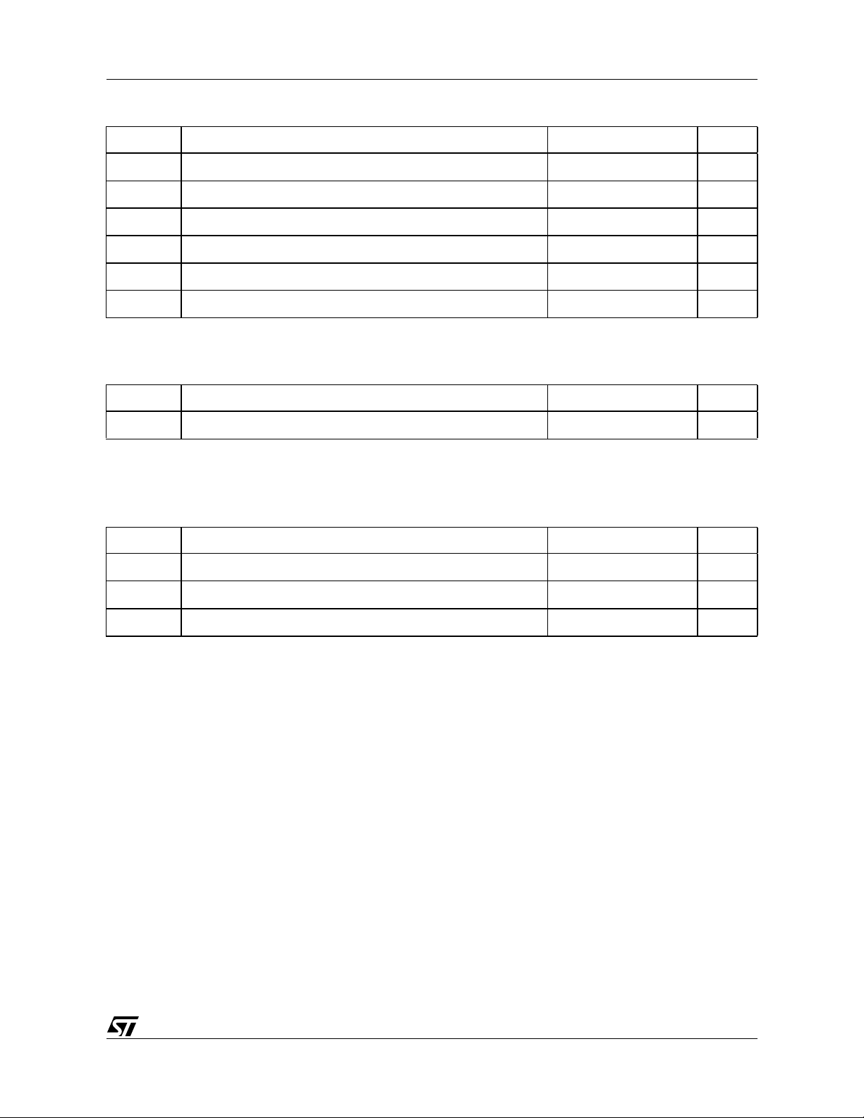
Table 3. Interface format as a function of SAI bits.
SAI(2..0) Interface Format
000
2
S
I
001 Left-Justified Data
010 Right-Justified 16-bit Data
011 Right-Justified 18-bit Data
100 Right-Justified 20-bit Data
101 Right-Justified 24-bit Data
Figure 2. Seri al Audio Signals
SAI=000 I2S
LRCLK
SCLK
SDATA
SAI=001 Left Justified
LRCLK
Left Right
LSB MSB LSB MSB MSB
Left Right
SCLK
SDATA
SAI=010 to 101 Right Justified
LRCLK
SCLK
SDATA
Left Right
LSB MSB LSB MSB MSB
LSB MSB LSB MSB MSB
13/33
Page 14

STA308
3.1.3 Serial Audio Input Interface First Bit
BIT R/W RST NAME DESCRIPTION
5 R/W 0 SAIFB Determines MSB or LSB first for all SAI formats
0 – MSB First, 1 – LSB First
3.1.4 Zero-Crossing Volume Enable
BIT R/W RST NAME DESCRIPTION
6 R/W 1 ZCE Zero-Crossing Volume Enable :
1 – Volume adjustments will only occur at digital zero-crossings
0 – Volume adjustments will occur immediately
The ZCE bit enables zero-crossing volume adjustments. When volume is adjusted on digital zero-crossings,
"zipper noise" is eliminated
3.1.5 Dynamic Range Compression/Anti-Clipping Bit
BIT R/W RST NAME DESCRIPTION
6 R/W 0 DRC Dynamic Range Compression/A nti-C lippin g
0 – Limiters act in Anti-Clipping Mode
1- Limiters act in Dynamic Range Compression Mode
Both limiters can be used in one of two way s, anti-clipping or dynamic range compression. W hen used in anticlipping mode the limiter threshold values are constant and dependent on the gain/attenuation settings applied
to the input signal. In dynamic range compression mode the limiter threshold values vary with the volume settings allowing for limiting to occur independently of the gain/attenuation but dependent on the input signal
3.2 Configuration Register C (address 02h)
BIT D7 D6 D5 D4 D3 D2 D1 D0
NAME HPB CSZ4 CSZ3 CSZ2 CSZ1 CSZ0 OM1 OM0
RST 01 1 11100
3.2.1 DDX Pow e r Ou t put Mode
BIT R/W RST NAME DESCRIPTION
0 R/W 0 OM0 DDX Power Output Mode : Selects configuration of DDX output.
1 R/W 0 OM1
The DDX Power Output Mode selects how the DDX output timing is configur ed. Dif ferent power devices us e
different output modes. The DDX recommended use is OM = 00. The variable mode uses the OMVx bits for
adjustment
OM(1,0) Output Stage - Mode
00 Fixed Compensation for DDX-2060, DDX-2100 power amplifiers
01 Tapered Compensation for Discrete Output Stage
10 Full Power Mode
11 Variable Compensation (CSZx bits, see 3.3.2)
14/33
Page 15

3.2.2 DDX Compensating Pulse Size Register
BIT R/W RST NAME DESCRIPTION
STA308
2 R/W 1 CSZ0 Contra Size Register : When OM(1,0) = 11, this register determines the
3 R/W 1 CSZ1
4 R/W 1 CSZ2
5 R/W 1 CSZ3
6 R/W 1 CSZ4
CSZ(4..0) Compensating Pulse Size
00000 0 Clock period Compensating Pulse Size
00001 1 Clock period Compensating Pulse Size
……
11111 31 Clock period Compensating Pulse Size
size of the DDX compensating pulse from 0 clock ticks to 31 clock periods.
3.2.3 High-Pass Filter Bypass
BIT R/W RST NAME DESCRIPTION
7 R/W 0 HPB High-Pass Filter Bypass Bit. Setting of one bypasses internal AC
coupling digital high-pass filter
The STA308 features an internal digital high-pass filter for the purpose of AC coupling. The purpose of this filter
is to prevent DC signals from passing through a DDX amplifier. DC signals can cause speaker damage
3.3 Configuration Register D (address 03h)
BIT D7 D6 D5 D4 D3 D2 D1 D0
NAME BQL PSL COS1 COS0 C78BO C56BO C34BO C12BO
RST 00 1 00000
3.3.1 Binary Output Enable Registers
BIT R/W RST NAME DESCRIPTION
0 R/W 0 C12BO Channels 1&2, 3&4, 5&6, 7&8 Binary Output Mode Enable
1 R/W 0 C34BO
2 R/W 0 C56BO
3 R/W 0 C78BO
Bits. A setting of 0 indicates ordinary DDX tri-state output. A
setting of 1 indicates binary output mode.
Each two-channel pair of outputs can be set to output a binary PWM stream. In this mode, output A
of a channel will be considered the positive output and output B is negative inverse. For example, setting C34BO
= 1 sets channels 3&4 to Binary Output (PWM) Mode.
3.3.2 Clock Output Select
BIT R/W RST NAME DESCRIPTION
4 R/W 0 COS0 Clock Output Select
5 R/W 1 COS1 Clock Output Select
15/33
Page 16

STA308
The Clock Output Select register selects the frequency of the clock output pin relative to the PLL clock output.
The PLL clock runs at 2048fs for 32, 44.1, and 48kHz, at 1024fs for 88.2kHz and 96 kHz, and at 512fs for
176.4kHz and 192kHz.
COS(1,0) CKOUT Frequency
01 PLL Output/4
10 PLL Output/8
11 PLL Output/16
3.3.3 Post-Scale Link
BIT R/W RST NAME DESCRIPTION
6 R/W 0 PSL Post-Scale Link :0 – Each Channel uses individual Post-Scale value
1 - Each Channel uses Channel 1 Post-Scale value
For multi-channel applications, the post-scale values can be linked to the value of channel 1 for ease of use and
update the values faster.
3.3.4 Biquad Coef ficient Link
BIT R/W RST NAME DESCRIPTION
7 R/W 0 BQL Biquad Link :
0 – Each Channel uses coefficient values
1- Each Channel uses Channel 1 coefficient values
For ease of use, all channels can use the biquad coefficients loaded into the Channel 1 Coefficient RAM space
by setting the BQL bit to 1. Then any EQ updates would only have to be performed once.
3.4 Configuration Register E (addre ss 04h)
BIT D7 D6 D5 D4 D3 D2 D1 D0
NAME DCV SAOFB SAO2 SAO1 SAO0 DEMP VOLEN MIXE
RST 00 0 00010
BIT R/W RST NAME DESCRIPTION
0 R/W 0 MIXE Mix Enable: 0 – Normal Operation
1 - Adjacent Channel Mix Mode
The scale and mix functionality can be used to mix adjacent channels instead of for bass management. By setting this bit(BME must be set to 0) odd channels will be mixed with their adjacent even channel and output in
the place of the even channel. The odd channel wills pass-through unscaled. The values used for this function
are the same as for bass management. Since this function occurs pos t channel mapping a l arge number of
possibilities are present for two channel mixing. Up to four mixed channels can be obtained.
BIT R/W RST NAME DESCRIPTION
1 R/W 1 VOLEN Volume Enable: 0 – Volume Operation Bypassed
1 - Volume Operation Normal
When VOLEN set to 1, volume operation is normal. When set to 0, volume operation is bypassed and the volume stages are all set to pass-through. This also eliminates the digital volume offset of ~-0.6dB that is used to
16/33
Page 17

STA308
map full-scale digital input to full DDX modulation output.
BIT R/W RST NAME DESCRIPTION
2 R/W 0 DEMP Deemphasis : 0 – No Deemphasis, 1- Deemphasis
By setting this bit to one deemphasis will implemented on all channels. When this is used it takes the place of
biquad #1 in each channel and any coefficients using biquad #1 will be ignored. DSP B(D SP Bypass) bit must
be set to 0 fo r De e mphasis to function.
BIT R/W RST NAME DESCRIPTION
3 R/W 0 SAO0 Serial Audio Output Interface Format : Determines the interface
4 R/W 0 SAO1
5 R/W 0 SAO2
The STA308 features a configurable digital serial audio interface. The settings of the SAIx bits determine how
the output to this interface is interpreted. Six formats are accepted.
Table 4. Interface format as a function of SAO bits.
SAO(2..0) Interface Format
000
001 Left-Justified Data
010 Right-Justified 16-bit Data
011 Right-Justified 18-bit Data
100 Right-Justified 20-bit Data
101 Right-Justified 24-bit Data
2
I
S
format of the output serial digital audio interface.
BIT R/W RST NAME DESCRIPTION
6 R/W 0 SAOFB Determines MSB or LSB first for all SAO formats;
0 – MSB First
1 – LSB First
BIT R/W RST NAME DESCRIPTION
7 R/W 0 DCV Distortion Compensation Variable:
0 – Use Standard DC Coefficient
1- Use DCC bits for DC Coefficient
3.5 Configuration Register F (address 05h)
BIT D7 D6 D5 D4 D3 D2 D1 D0
NAME EAPD AME COD SID PWMD
RST 00000
BIT R/W RST NAME DESCRIPTION
0 R/W 0 PWMD PWM Output Disable: 0 – PWM Output Normal
1- No PWM Output
17/33
Page 18

STA308
1 R/W 0 SID
2 R/W 0 COD Clock Output Disable: 0 – Clock Output Normal
3 R/W 0 AME AM Mode Enable : 0 – Normal DDX operation.
Serial Interface(I
1- No I
1- No Clock Output
1 – AM reduction mode DDX operation.
2
S Out) Disable: 0 – I2S Output Normal
2
S Output
The STA308 features a DDX processing mode that minimizes the amount of noise generated in frequency range
of AM radio. This mode is intended to be used when DDX is operating in a device with an AM tuner active. The
SNR of the DDX processing is reduced to ~83dB in this mode, which is still greater than the SNR of AM radio.
BIT R/W RST NAME DESCRIPTION
7 R/W 0 EAPD External Amplifier Power Down:
0 – External Power Stage Power Down Active
1 - Normal Operation
This output bit, on pin 51 of the device, is used to mute the DDX Power Devices for Power-Down.
3.6 Master Mute Register (address 06h)
BIT D7 D6 D5 D4 D3 D2 D1 D0
NAME MMUTE
RST 0
3.7 Master Volume Register (addre ss 07h)
BIT D7 D6 D5 D4 D3 D2 D1 D0
NAME MV7 MV6 MV5 MV4 MV3 MV2 MV1 MV0
RST 11 1 11111
3.8 Channels 1,2,3,4,5,6,7,8 Mute (address 08h)
BIT D7 D6 D5 D4 D3 D2 D1 D0
NAME C8M C7M C6M C5M C4M C3M C2M C1M
RST 00 0 00000
3.9 Channel 1 Volume (address 09h )
BIT D7 D6 D5 D4 D3 D2 D1 D0
NAME C1V7 C1V6 C1V5 C1V4 C1V3 C1V2 C1V1 C1V0
RST 00 1 10000
3.10 Channe l 2 Volume (address 0Ah)
BIT D7 D6 D5 D4 D3 D2 D1 D0
NAME C2V7 C2V6 C2V5 C2V4 C2V3 C2V2 C2V1 C2V0
RST 00 1 10000
18/33
Page 19

STA308
3.11 Chann el 3 Volume (address 0Bh)
BIT D7 D6 D5 D4 D3 D2 D1 D0
NAME C3V7 C3V6 C3V5 C3V4 C3V3 C3V2 C3V1 C3V0
RST 0 01 10000
3.12 Chann el 4 Volume (address 0Ch)
BIT D7 D6 D5 D4 D3 D2 D1 D0
NAME C4V7 C4V6 C4V5 C4V4 C 4V3 C4V2 C4V1 C4V0
RST 00 1 10000
3.13 Chann el 5 Volume (address 0Dh)
BIT D7 D6 D5 D4 D3 D2 D1 D0
NAME C5V7 C5V6 C5V5 C5V4 C 5V3 C5V2 C5V1 C5V0
RST 00 1 10000
3.14 Chann el 6 Volume (address 0Eh)
BIT D7 D6 D5 D4 D3 D2 D1 D0
NAME C6V7 C6V6 C6V5 C6V4 C 6V3 C6V2 C6V1 C6V0
RST 00 1 10000
3.15 Chann el 7 Volume (address 0Fh)
BIT D7 D6 D5 D4 D3 D2 D1 D0
NAME C7V7 C7V6 C7V5 C7V4 C 7V3 C7V2 C7V1 C7V0
RST 00 1 10000
3.16 Chann el 8 Volume (address 10h)
BIT D7 D6 D5 D4 D3 D2 D1 D0
NAME C8V7 C8V6 C8V5 C8V4 C 8V3 C8V2 C8V1 C8V0
RST 00 1 10000
The Volume structure of the STA308 consists of individual volume registers for each channel and a master volume register that provides an offset to each channels volume setting. The individual channel volumes are adjustable in 0.5dB steps from +24dB to -103dB. As an example if C5V = 0Bh or +18.5dB and MV = 21h or -
16.5dB, then the total gain for channel 5 = +2dB. The Master Mute when set to 1 will mute all channels at once,
whereas the individual channel mutes(CxM) will mute only that channel. Both the Master Mute and the Channel
Mutes provide a "soft mute" wi th the volume ramping down to mute in 8192 samples from t he maxim um volume
setting at the internal processing rate(~192kHz). A "hard mute" can be obtained by commanding a value of all
1's(255) to any channel volume register or the master volume register. When volume offsets are provided via
the master volume register any channel that whose total volume is less than -103dB will be muted. All changes
in volume take place at zero-crossings when ZCE = 1(configuration regi ster B) on a per channel basis as t his
creates the smoothest possible volume transitions. When ZCE=0, volume updates will occur immediately.
19/33
Page 20

STA308
Table 5. Master Volume Offset as a function of MV(7..0).
MV(7..0) Volume Offset from Channel Value
00000000(00h) 0dB
00000001(01h) -0.5dB
00000010(02h) -1dB
……
01001100(4Ch) -38dB
……
11111110(FEh) -127dB
11111111 (FFh) Hard Master Mute
Channel Volume as a function of CxV(7..0)
CxV(7..0) Volume
00000000(00 h) +24dB
00000001(01 h) +23.5dB
00000010(02 h) +23dB
……
00101111(2Fh) +0.5dB
00110000(30h) 0dB
00110001(31h) -0.5d B
……
1111111 0(FEh ) -103d B
11111111(FFh) Hard Channel Mute
3.17 Channel Input Mapping Channels 1 & 2 (address 11h)
BIT D7 D6 D5 D4 D3 D2 D1 D0
NAME C2IM2 C2IM1 C2IM0 C1IM2 C1IM1 C1IM0
RST 00 1 000
3.18 Channel Input Mapping Channels 3 & 4 (address 12h)
BIT D7 D6 D5 D4 D3 D2 D1 D0
NAME C4IM2 C4IM1 C4IM0 C3IM2 C3IM1 C3IM0
RST 01 1 010
3.19 Channel Input Mapping Channels 5 & 6 (address 13h)
BIT D7 D6 D5 D4 D3 D2 D1 D0
NAME C6IM2 C6IM1 C6IM0 C5IM2 C5IM1 C5IM0
RST 10 1 100
20/33
Page 21

STA308
3.20 Channel Input Mapping Channels 7 & 8 (address 14h)
BIT D7 D6 D5 D4 D3 D2 D1 D0
NAME C8IM2 C8IM1 C8IM0 C7IM2 C7IM1 C7IM0
RST 11 1 110
Each channel received via I2S can be mapped to any internal processing channel via the Channel Input Mapping registers. This allows f or fl exibi l ity i n proces sing, si mplif ies output stage desi gns, and enables t he abi l ity
to perform crossovers. The default settings of these registers map each I2S input channel to its corresponding
processing channel.
For example, to map input 2 to Channel 5, set Address 11h, bits D6, D5 and D4 to 100. Now, inputs 2 and 5 go
to Channel 5.
Table 6. Channel Mapping as a function of CxIM bits
CxIM(2..0)
000 Channel 1
001 Channel 2
010 Channel 3
011 Cha nnel 4
100 Channel 5
101 Channel 6
110 Cha nnel 7
111 Channel 8
2
S Input Mapped to:
I
Channel 1
Channel 2
Channel 3
Channel 4
Channel 5
Channel 6
Channel 7
Channel 8
CxIM(2..0)
8:1
Mux
3
Channel X
DDX-8000 Output Phasing
CH1
CH2
CH3
CH4
CH5
CH6
CH7
CH8
1/384kHz or 2.874us
21/33
Page 22

STA308
3.21 Ch annel Limiter Select Channels 1,2,3,4 (address 15h)
BIT D7 D6 D5 D4 D3 D2 D1 D0
NAME C4LS1 C4LS0 C3LS1 C3LS0 C2LS1 C2LS0 C1LS1 C1LS0
RST 00 0 00000
3.22 Ch annel Limiter Select Channels 5,6,7,8 (address 16h)
BIT D7 D6 D5 D4 D3 D2 D1 D0
NAME C8LS1 C8LS0 C7LS1 C7LS0 C6LS1 C6LS0 C5LS1 C5LS0
RST 00 0 00000
3.23 Limiter 1 Attack/Release Rate (address 17h)
BIT D7 D6 D5 D4 D3 D2 D1 D0
NAME L1R3 L1R2 L1R1 L1R0 L1A3 L1A2 L1A1 L1A0
RST 10 1 00110
3.24 Limiter 1 Attack/Release Threshold (address 18h)
BIT D7 D6 D5 D4 D3 D2 D1 D0
NAME L1AT3 L1AT2 L1AT1 L1A T0 L1RT3 L1RT2 L1RT1 L1RT0
RST 01 1 00111
3.25 Limiter 2 Attack/Release Rate (address 19h)
BIT D7 D6 D5 D4 D3 D2 D1 D0
NAME L2R3 L2R2 L2R1 L2R0 L2A3 L2A2 L2A1 L2A0
RST 10 1 00110
3.26 Limiter 2 Attack/Release Threshold (address 1Ah)
BIT D7 D6 D5 D4 D3 D2 D1 D0
NAME L2AT3 L2AT2 L2AT1 L2A T0 L2RT3 L2RT2 L2RT1 L2RT0
RST 01 1 00111
22/33
Page 23

STA308
Basic Limiter and Volume Flow Diagram
Gain/Volume
Input Output
Gain Attenuation Saturation
.
RMSLimiter
A limiter is basically a variable gain device, where the amount of gain applied depends on the input signal level.
As the name implies, compression limits the dynamic range of the signal.
The STA308 includes 2 independent limiter blocks. The purpose of the l i miters is to aut omaticall y r educe the
dynamic range of the input signal to prevent the outputs from clipping in anti-clipping mode or to actively reduce
the dynamic range for a better listening environment such as a night-time listening mode which is often needed
for DVDs. The two modes are selected via the DRC bit in Configuration Register B; address 0x02, bit 7.
Each channel can be mapped to either limiter or not mapped. Non-mapped channels will clip when 0dBFS is
exceeded. Each limiter will loo k at the pres en t valu e o f each channel that is mapped to it, select the maximum
absolute value of all these channels, perform the limiting algorithm on that value, and then, if needed, adjust the
gain of the mapped channels in unison.
The limiter attack thresholds are determined by the LxAT registers. It is recommended in anti-clipping mode to
set this to 0dBFS, which corresponds to the maximum unclipped output power of a DDX amplifier. Since gain
can be added digitally within the STA308 it is possible to exceed 0dBFS or any other LxAT setting. When this
occurs, the limiter, when active, will automatically start reducing the gain. The rate at which the gain is reduced
when the attack threshol d i s exc eeded i s dependent upon t he att ack rate register set ti ng f or t hat limiter. The
gain reduction occurs on a peak-detect algorithm.
The release of limiter (uncompression), when the gain is again increased, is dependent on a RM S-detect algorithm. The output of the volume/limiter block is passed through a RMS filter. The output of this filter is compared
to the release threshold, determined by the Release Threshold register. When the RMS filter output falls below
the release threshold, the gain is again increased (uncompressed) at a rate dependent upon the Release Rate
register. The gain can never be increased past its set value and therefore the release will only occur if th e lim iter
has already reduced the gain. The release threshold value can be used to set what is effectively a minimum
dynamic range, this is helpful as over-limiting can reduce the dynamic range to virtually zero and cause program
material to sound "lifeless". In AC mode the attack and release thresholds are set relative to full-scale. In DRC
mode the attack threshold is set relative to the maximum volume setting of the channels mapped to that limiter
and the release threshold is set relative to the maximum volume setting plus the attack threshold.
Table 7. Channel Limiter Mapping as a function of CxLS bits.
CxLS(1,0) Channel Limiter Mapping
00 Channel has limiting disabled
01 Channel is mapped to limiter #1
10 Channel is mapped to limiter #2
23/33
Page 24

STA308
Table 8. Limiter Attack Rate as a function of LxA bits.
LxA(3..0) Attack Rate dB/ms
0001
0010
0011
LxA(3..0) 1.3536
0000 0.9024
0110
0111 0.2256
1000 0.1504
1001 0.1123
1010 0.0902
1011 0.0752
1100 0.0645
1101 0.0564
1110 0.0501
1111 0.0451
note: Shad ed areas are Default Setti ngs
0.4512
Table 9. Limiter Release Rate and Uncompression Threshold as a function of LxR bits
LxR(3..0) Release Rate dB/ms
0000 0.5116
0001 0.1370
0010 0.0744
0011 0.0499
0100 0.0360
0101 0.0299
0110 0.0264
0111 0.0208
1000 0.0198
1001 0.0172
1010
1011 0.0137
1100 0.0134
1101 0.0117
1110 0.0110
1111 0.0104
0.0147
24/33
Page 25

Table 10. Limiter Attack Threshold as a function of LxAT bits.
LxAT(3..0) AC(dB relative to FS) DRC(db relative to Volume)
0000 -12 -22
0001 -10 -20
0010 -8 -18
0011 -6 -16
0100 -4 -14
0101 -2 -12
STA308
0110
0111 +2 -8
1000 +3 -7
1001 +4 -6
1010 +5 -5
1011 +6 -4
1100 +7 -3
1101 +8 -2
1110 +9 -1
1111 +10 0
0 -10
Table 11. Limiter Release Threshold as a function of LxRT bits
LxRT(3..0) AC(dB relative to FS) DRC(db relative to Volume + LxAT)
0000 • •
0001 -23dB -33dB
0010 -16.9dB -26.9dB
0011 -13.4dB -23.4dB
0100 -10.9dB -20.9dB
0101 -9.0dB -19.0dB
0110 -7.4dB -17.4dB
0111
1000 -4.9dB -14.9dB
1001 -3.8dB -13.8dB
1010 -2.9dB -12.9dB
1011 -2.1dB -12.1dB
1100 -1.3dB -11.3dB
1101 -0.65dB -10.65dB
1110 0dB -10dB
1111 +0.6dB -9.4dBdB
-6.0dB -16.0dB
25/33
Page 26

STA308
3.27 Bas s and Treble Tone Con trol(address 1Bh)
BIT D7 D6 D5 D4 D3 D2 D1 D0
NAME TTC3 TTC2 TTC1 TTC0 BTC3 BTC2 BTC1 BTC0
RST 01 1 10111
The STA308 contains bass and treble tone control adjustments. These are selectable from +12dB to -12dB of
boost or cut. These are 1st order shelving filters with a corner frequency of 150Hz for bass and 3kHz for treble.
Any gain introduced in the tone controls will carry through to the volume and limiting block without saturation.
Table 12. Ton e Cont rol Boost/ Cut as a fu nct i on of BTC and TTC bits
BTC(3..0)/TTC(3..0) Boost/Cut
0000 -12dB
0001 -12dB
……
0111 -4dB
01 10 -2dB
0111 0dB
1000 +2dB
1001 +4dB
……
1 101 +12dB
1110 +12dB
1111 +12dB
3.28Coefficient Address Register (address 1Ch)
BIT D7 D6 D5 D4 D3 D2 D1 D0
NAME CFA7 CFA6 CFA5 CFA4 CFA3 CFA2 CFA1 CF A0
RST 00 0 00000
3.29 Coefficien t b2 Data Register Bits 23..16 (address 1Dh)
BIT D7 D6 D5 D4 D3 D2 D1 D0
NAME C1B23 C1B22 C1B21 C1B20 C1B19 C1B18 C1B17 C1B16
RST 00 0 00000
3.30 Coefficien t b2 Data Register Bits 15..8 (address 1Eh)
BIT D7 D6 D5 D4 D3 D2 D1 D0
NAME C1B15 C1B14 C1B13 C1B12 C1B11 C1B10 C1B9 C1B8
RST 00 0 00000
3.31Coefficient b2 Data Register Bits 7..0 (address 1Fh)
BIT D7 D6 D5 D4 D3 D2 D1 D0
NAME C1B7 C1B6 C1B5 C1B4 C1B3 C1B2 C1B1 C1B0
RST 00 0 00000
26/33
Page 27

STA308
3.32 Coefficien t b0 Data Register Bits 23..16 (address 20h)
BIT D7 D6 D 5 D4 D3 D2 D1 D0
NAME C2B 23 C2B22 C2B21 C2B20 C2B19 C2B18 C2B17 C2B16
RST 00 0 00000
3.33 Coefficien t b0 Data Register Bits 15..8 (address 21h)
BIT D7 D6 D 5 D4 D3 D2 D1 D0
NAME C2B 15 C2B14 C2B13 C2B12 C2B11 C2B10 C2B9 C2B8
RST 00 0 00000
3.34Coefficient b0 Data Register Bits 7..0 (address 22h)
BIT D7 D6 D 5 D4 D3 D2 D1 D0
NAME C2B7 C2B6 C2B5 C2B4 C 2B3 C2B2 C2B1 C2B0
RST 00 0 00000
3.35 Coefficien t a2 Data Register Bits 23..16 (address 23h)
BIT D7 D6 D 5 D4 D3 D2 D1 D0
NAME C3B 23 C3B22 C3B21 C3B20 C3B19 C3B18 C3B17 C3B16
RST 00 0 00000
3.36 Coefficien t a2 Data Register Bits 15..8 (address 24h)
BIT D7 D6 D 5 D4 D3 D2 D1 D0
NAME C3B 15 C3B14 C3B13 C3B12 C3B11 C3B10 C3B9 C3B8
RST 00 0 00000
3.37 Coefficient a2 Data Register Bits 7..0 (address 25h)
BIT D7 D6 D 5 D4 D3 D2 D1 D0
NAME C3B7 C3B6 C3B5 C3B4 C 3B3 C3B2 C3B1 C3B0
RST 00 0 00000
3.38 Coefficien t a1 Data Register Bits 23..16 (address 26h)
BIT D7 D6 D 5 D4 D3 D2 D1 D0
NAME C4B 23 C4B22 C4B21 C4B20 C4B19 C4B18 C4B17 C4B16
RST 00 0 00000
3.39 Coefficien t a1 Data Register Bits 15..8 (address 27h)
BIT D7 D6 D 5 D4 D3 D2 D1 D0
NAME C4B 15 C4B14 C4B13 C4B12 C4B11 C4B10 C4B9 C4B8
RST 00 0 00000
27/33
Page 28

STA308
3.40 Coefficient a1 Data Register Bits 7..0 (address 28h)
BIT D7 D6 D 5 D4 D3 D2 D1 D0
NAME C4B7 C4B6 C4B5 C4B4 C 4B3 C4B2 C4B1 C4B0
RST 00 0 00000
3.41 Coefficien t b1 Data Register Bits 23..16 (address 29h)
BIT D7 D6 D 5 D4 D3 D2 D1 D0
NAME C5B 23 C5B22 C5B21 C5B20 C5B19 C5B18 C5B17 C5B16
RST 00 0 00000
3.42 Coefficien t b1 Data Register Bits 15..8 (address 2Ah)
BIT D7 D6 D 5 D4 D3 D2 D1 D0
NAME C5B 15 C5B14 C5B13 C5B12 C5B11 C5B10 C5B9 C5B8
RST 00 0 00000
3.43Coefficient b1 Data Register Bits 7..0 (address 2Bh)
BIT D7 D6 D 5 D4 D3 D2 D1 D0
NAME C5B7 C5B6 C5B5 C5B4 C 5B3 C5B2 C5B1 C5B0
RST 00 0 00000
3.44 Coefficien t Write Control Register (address 2Ch)
BIT D7 D6 D 5 D4 D3 D2 D1 D0
NAME WA W1
RST
Coefficients for EQ and Bass Management are handled internally in the STA308 via RAM. Access to this RAM
is available to the user via an I2C register i nterf ace. A col lecti on of I2C regist ers is dedi cated to thi s f unction.
One contains a coefficient base address, five sets of three store the values of the 24-bit coefficients to be written
or that were read, and one contains bits used to control the writing of the coefficient(s) to RAM. The following
are step instructions for reading and writing coefficients.
Reading a coefficient from RAM
– write 8-bit address to I2C register 1Ch
– ead top 8-bits of coefficient in I2C address 1Dh
– ead middle 8-bits of coefficient in I2C address 1Eh
– ead bottom 8-bits of coefficient in I2C address 1Fh
Writing a single coefficient to RAM
– write 8-bit address to I2C register 1Ch
– write top 8-bits of coefficient in I2C address 1Dh
– write middle 8-bits of coefficient in I2C address 1Eh
– write bottom 8-bits of coefficient in I2C address 1Fh
– write 1 to W1 bit in I2C address 2Bh
28/33
Page 29

STA308
Writing a set of coefficients to RAM
– write 8-bit starting address to I2C register 1Ch
– write top 8-bits of coefficient b2 in I2C address 1Dh
– write middle 8-bits of coefficient b2 in I2C address 1Eh
– write bottom 8-bits of coefficient b2 in I2C address 1Fh
– write top 8-bits of coefficient b0 in I2C address 20h
– write middle 8-bits of coefficient b0 in I2C address 21h
– write bottom 8-bits of coefficient b0 in I2C address 22h
– write top 8-bits of coefficient a2 in I2C address 23h
– write middle 8-bits of coefficient a2 in I2C address 24h
– write bottom 8-bits of coefficient a2 in I2C address 25h
– write top 8-bits of coefficient a1 in I2C address 26h
– write middle 8-bits of coefficient a1 in I2C address 27h
– write bottom 8-bits of coefficient a1 in I2C address 28h
– write top 8-bits of coefficient b1 in I2C address 29h
– write middle 8-bits of coefficient b1 in I2C address 2Ah
– write bottom 8-bits of coefficient b1 in I2C address 2Bh
– write 1 to WA bit in I2C address 2Ch
The mechanism for writing a set of coefficients to RAM provides a method of updating the five coefficients corresponding to a given biquad (filter) si multaneousl y to avoi d possibl e unpleasant ac oustic s ide effect s. When
using this technique, the 8-bit address would specify the address of the biquad b2 coefficient (e.g. 0, 5, 10, 15,
…, 50, … 195 decimal), and the STA308 wi ll generate the RAM addresses as of fsets f rom thi s bas e val ue t o
write the complete set of coefficient data.
Equalization:
Figure 3. Data Flow for single channel Biquad / Bass / Treble block.:
From
1st Interpolation
Stage
PreScale Biquad1 Biquad2 Biquad3 Biquad4 Biquad5
To
Volume/
Limiter
Bass/
Treble
Five user-programmable 28-bit biquads are available per channel in the STA308. These biquads run at 192kHz
for 48kHz, 96kHz, or 192kHz input and at 176.4kHz for 44.1kHz, 88.2kHz, and 176.4kHz input. The PreScale
block is used for at tenuation when fi lters are to be designed t hat boost frequenc ies above 0dBFS. This is a
single 28-bit signed multiply, with 800000h = -1 and 7FFFFFh = 0.9999998808. These values are labeled
CxPS, with x representing the channel. The biquads use this equation:
Y[n] = 2(b0/2)X[n] + 2(b1/2)X[n-1] + b2X[n-2] - 2(a1/2)Y[n-1] - a2Y[n-2]
= b0X[n] + b 1 X[n-1] + b2X[n-2] - a1Y[n-1 ] - a 2 Y[n-2]
29/33
Page 30

STA308
Y[n] represents the output and X[n] represents the input. Coefficients are defined in the following manner:
CxHx0 = b2
CxHx1 = b0/2
CxHx2 = -a2
CxHx3 = -a1/2
CxHx4 = b1/2
The first x represents the channel and the second the biquad number. For example C3H41 is the b0/2 coefficient in the fourt h seri es biquad in channel 3. The bi quad l ink bit al l ows all channel s t o use t he coef fi cients of
channel 1.
Bass Management
Channel 6 provides the ability to scale and mix all channels before the biquad block. This allows for information
from any channel to be redirected t o this channel and then fi ltered appropri ately for a subwoofer appli cation.
When the BME bit is set (bit D5 of Configuration Register A, at address 00h) the input to the biquad section is
routed from the scale and mix block instead of the normal channel 6 1st stage interpolation output. Eight scaling
coefficients are provided to perform this function. They are labeled CxBMS with x representing the channel that
is being scaled. Each input channel is multiplied by its corresponding scale factor and summed. The output of
the summation is the output of the scale and mix block.
Post-Scale
The STA308 provides one additional multiplication aft er the last interpolati on stage and before the distortion
compensation on each channel. This is a 24-bit signed fractional multiply. The scale factor f or this multipl y is
loaded into RAM using the same I2C registers as the biquad coefficients and the bass-management. All channels can use the channel 1 by setting the post-scale link bit.
RAM Block for Biquads and Bass Management:
Index
(Decimal)
0 00h Channel 1 - Biquad 1 C1H10(b
1 01h C1H11(b0/2) 3FFFFFh
2 02h C1H12(a2) 000000h
3 03h C1H13(a1/2) 000000h
4 04h C1H14(b1/2) 000000h
5 05h Channel 1 - Biquad 2 C1H20 000000h
……… … …
24 18h Channel 1 - Biquad 5 C1H54 000000h
25 19h Channel 2 - Biquad 1 C2H10 000000h
Index
(Hex)
Coefficient Default
2)
000000h
26 1Ah C2H11 3FFFFFh
……… … …
30/33
Page 31

STA308
45 2Dh Distortion Compensation DCC 23…0 000000h
……… … …
49 31h Channel 2 - Biquad 5 C2H54 000000h
50 32h Channel 3 - Biquad 1 C3H10 000000h
……… … …
199 C7h Channel 8 - Biquad 5 C8H54 000000h
200 C8h Channel 1 - Pre-Scale C1PS 800000h
201 C9h Channel 2 – Pre-Scale C2PS 800000h
202 CAh Channel 3 – Pre-Scale C3PS 800000h
……… … …
207 CFh Channel 8 –Pre-Scale C8PS 800000h
208 D0h Channel 1 – BassM Scale C1BMS 000000h
209 D1h Channel 2 – BassM Scale C2BMS 000000h
……… … …
215 D7h Channel 8 – BassM Scale C8BMS 000000h
216 D8h Channel 1 – Post-Scale C1PS 800000h
217 D9h Channel 2 – Post-Scale C2PS 800000h
……… … …
223 DFh Channel 8 – Post-Scale C8PS 800000h
224 F0h Not Used
……… … …
255 FFh Not Used
31/33
Page 32

STA308
DIM.
mm inch
MIN. TYP. MAX. MIN. TYP. MAX.
A 1.60 0.063
A1 0.05 0.15 0.002 0.006
A2 1.35 1.40 1.45 0.053 0.055 0.057
B 0.18 0.23 0.28 0.007 0.009 0.011
C 0.12 0.16 0.20 0.0047 0.0063 0.0079
D 12.00 0.472
D1 10.00 0.394
D3 7.50 0.295
e 0.50 0.0197
E 12.00 0.472
E1 10.00 0.394
E3 7.50 0.295
L 0.40 0.60 0.75 0.0157 0.0236 0.0295
L1 1.00 0.0393
K 0°(min.), 7°(max.)
OUTLINE AND
MECHANICAL DATA
TQFP64
D
D1
A1
TQFP64
3348
32
E3D3E1
17
16
E
L1
L
0.10mm
Seating Plane
B
K
49
B
64
1
e
A
A2
C
32/33
Page 33

STA308
Information furnished is believed to be accurate and reliable. However, STMicroelectronics assumes no responsibility for the consequences
of use of such information nor for any infringement of patents or other rights of third parties which may result from its use. No license is granted
by implic ation or otherwise under any patent or patent r i ght s of STMi croelectr oni cs. Spec i fications mentioned i n this publication are s ubj ect
to change without notice. This publication supersedes and replaces all information previously supplied. STMicroelectronics product s are not
authorized for use as cri tical comp onents in lif e support devi ces or systems without express written approva l of STMicroel ectronics.
The ST logo is a registered trademark of STMicroelectronics
2002 STMicroelectroni cs - All Righ ts Reserved
DDX is a trademark of Apogee Technol ogy inc.
Austra lia - Brazil - Canada - Chi na - F i nl and - Franc e - Germany - Hong Kong - In di a - Israel - Ita l y - J apan -Malaysia - Malta - Morocco -
Singap ore - Spain - Sw eden - Switze rl and - Unit ed K i ngdom - United States .
STMicroelectronics GROUP OF COMPANIES
http://www.s t. com
33/33
 Loading...