

Page 1

infotainment application processor with embedded GPS
Features
■
ARM1176 533 MHz host processor
– Cache: 32 KB instruction, 32 KB data
– Vector floating point unit
■ High performance embedded GPS subsystem
– Parallel acquisition engines for 8 GPS
satellites or 4 Galileo satellites
– 32 tracking channels for all satellites in view
– 5 correlators per channel for urban canyon
robustness
– Multibit signal processing hardware
■ Advanced power management
– Separated power islands for ultra low
power mode
– Dynamic core frequency scaling
– 512-Byte embedded SRAM for back-up
■ System infrastructure
– LP DDR/DDR2 controller: 16 bit data
256 MB addressable (333 MHz DDR2,
200 MHz LPDDR)
– One bank of 32 KB embedded SRAM
– 64-channel vector interrupt controller (VIC)
– 2 DMA controllers, 16 physical channels
– 32 DMA request for each controller
– Two external DMA requests are supported
■ Display and graphics
– Color LCD controller for STN,TFT or HR-
TFT panels with 18-bit parallel RGB
interface
– Integrated touch screen controller and ADC
– 3D advanced graphics acceleration
– JPEG baseline profile decoder
■ High throughput interfaces
– 1 ports USB 2.0 OTG with integrated
physical layer
– 2 SD/MMC up to 8 bit data, all bootable
STA2064
Cartesio™ family
Data brief
TFBGA289 (15x15x1.2mm)
■ Audio interfaces and features
– Three multichannel serial ports (I2S/TDM)
– SPDIF input interface
– C3 hardware reed-solomon decoder
– Sample rate converter
■ Standard interfaces
– Four 16-bit input capture/output compare
– Pulse width light modulator (PWL)
– Four autobaud UART
– Three I
– Two synchronous serial port (SSP, SPI)
– 65 GPIO over 5 ports
■ One controller area network (CAN) in
automotive version
■ Programmable voltage IOs: 1.8 V, 2.5 V, 3.3 V
■ V
DDIO_ON
1.25 ±3%V
■ TFBGA 289, 0.8 mm pitch package, packing in
tray
■ Ambient temperature range: -40 / +85 °C
Table 1. Device summary
Order code
STA2064N Consumer 533 MHz No
STA2064A Automotive 533 MHz 1x
2
C multimaster/slave interfaces
: 1.8 ±10%V, V
Qualification
grade
: VDD,
DD_ON
CPU freq. CAN
October 2009 Doc ID 16057 Rev 3 1/19
For further information contact your local STMicroelectronics sales office.
www.st.com
19
Page 2

Contents STA2064
Contents
1 Description . . . . . . . . . . . . . . . . . . . . . . . . . . . . . . . . . . . . . . . . . . . . . . . . . 4
2 System description . . . . . . . . . . . . . . . . . . . . . . . . . . . . . . . . . . . . . . . . . . 5
2.1 MCU . . . . . . . . . . . . . . . . . . . . . . . . . . . . . . . . . . . . . . . . . . . . . . . . . . . . . . 5
2.2 Embedded memories . . . . . . . . . . . . . . . . . . . . . . . . . . . . . . . . . . . . . . . . . 5
2.2.1 Embedded SRAM (eSRAM) . . . . . . . . . . . . . . . . . . . . . . . . . . . . . . . . . . 5
2.3 System functions . . . . . . . . . . . . . . . . . . . . . . . . . . . . . . . . . . . . . . . . . . . . 5
2.3.1 System and reset controller (SRC) . . . . . . . . . . . . . . . . . . . . . . . . . . . . . 5
2.3.2 PMU . . . . . . . . . . . . . . . . . . . . . . . . . . . . . . . . . . . . . . . . . . . . . . . . . . . . . 5
2.3.3 DMA . . . . . . . . . . . . . . . . . . . . . . . . . . . . . . . . . . . . . . . . . . . . . . . . . . . . . 5
2.3.4 Vectored interrupt controller (VIC) . . . . . . . . . . . . . . . . . . . . . . . . . . . . . . 5
2.3.5 GPIOs . . . . . . . . . . . . . . . . . . . . . . . . . . . . . . . . . . . . . . . . . . . . . . . . . . . 5
2.3.6 Real-time clock (RTC) . . . . . . . . . . . . . . . . . . . . . . . . . . . . . . . . . . . . . . . 6
2.3.7 Real-time timer (RTT) . . . . . . . . . . . . . . . . . . . . . . . . . . . . . . . . . . . . . . . 6
2.3.8 Always_ON supply . . . . . . . . . . . . . . . . . . . . . . . . . . . . . . . . . . . . . . . . . . 6
2.3.9 Enhanced function timer (EFT) . . . . . . . . . . . . . . . . . . . . . . . . . . . . . . . . 6
2.3.10 Watchdog timer (WDT) . . . . . . . . . . . . . . . . . . . . . . . . . . . . . . . . . . . . . . 6
2.4 Memory interfaces . . . . . . . . . . . . . . . . . . . . . . . . . . . . . . . . . . . . . . . . . . . 6
2.4.1 SD/MMC . . . . . . . . . . . . . . . . . . . . . . . . . . . . . . . . . . . . . . . . . . . . . . . . . 6
2.4.2 DDR-SDRAM controller . . . . . . . . . . . . . . . . . . . . . . . . . . . . . . . . . . . . . . 7
2.5 Audio/video functions . . . . . . . . . . . . . . . . . . . . . . . . . . . . . . . . . . . . . . . . . 7
2.5.1 C3 . . . . . . . . . . . . . . . . . . . . . . . . . . . . . . . . . . . . . . . . . . . . . . . . . . . . . . 7
2.5.2 Sample rate converter (SaRaC) . . . . . . . . . . . . . . . . . . . . . . . . . . . . . . . 7
2.5.3 JPEG decoder . . . . . . . . . . . . . . . . . . . . . . . . . . . . . . . . . . . . . . . . . . . . . 7
2.5.4 Smart graphic accelerator (SGA) . . . . . . . . . . . . . . . . . . . . . . . . . . . . . . . 7
2.5.5 Color LCD controller (CLCD) . . . . . . . . . . . . . . . . . . . . . . . . . . . . . . . . . . 7
2.6 Communication interfaces . . . . . . . . . . . . . . . . . . . . . . . . . . . . . . . . . . . . . 8
2.6.1 USB . . . . . . . . . . . . . . . . . . . . . . . . . . . . . . . . . . . . . . . . . . . . . . . . . . . . . 8
2.6.2 UART . . . . . . . . . . . . . . . . . . . . . . . . . . . . . . . . . . . . . . . . . . . . . . . . . . . . 8
2.6.3 I2C . . . . . . . . . . . . . . . . . . . . . . . . . . . . . . . . . . . . . . . . . . . . . . . . . . . . . . 8
2.6.4 MSP . . . . . . . . . . . . . . . . . . . . . . . . . . . . . . . . . . . . . . . . . . . . . . . . . . . . . 8
2.6.5 SSP . . . . . . . . . . . . . . . . . . . . . . . . . . . . . . . . . . . . . . . . . . . . . . . . . . . . . 8
2.6.6 SPDIF . . . . . . . . . . . . . . . . . . . . . . . . . . . . . . . . . . . . . . . . . . . . . . . . . . . 8
2.6.7 AC97 controller . . . . . . . . . . . . . . . . . . . . . . . . . . . . . . . . . . . . . . . . . . . . 9
2/19 Doc ID 16057 Rev 3
Page 3

STA2064 Contents
2.6.8 CAN . . . . . . . . . . . . . . . . . . . . . . . . . . . . . . . . . . . . . . . . . . . . . . . . . . . . . 9
2.7 Specific functions . . . . . . . . . . . . . . . . . . . . . . . . . . . . . . . . . . . . . . . . . . . . 9
2.7.1 GPS . . . . . . . . . . . . . . . . . . . . . . . . . . . . . . . . . . . . . . . . . . . . . . . . . . . . . 9
2.7.2 Touchscreen controller/ADC . . . . . . . . . . . . . . . . . . . . . . . . . . . . . . . . . 10
2.7.3 Multisupply IO ring . . . . . . . . . . . . . . . . . . . . . . . . . . . . . . . . . . . . . . . . . 10
2.7.4 Driving strength and slew rate programmability . . . . . . . . . . . . . . . . . . . 11
3 System features introduction . . . . . . . . . . . . . . . . . . . . . . . . . . . . . . . . . 12
3.1 Power region partition . . . . . . . . . . . . . . . . . . . . . . . . . . . . . . . . . . . . . . . 12
3.2 Frequency region partition . . . . . . . . . . . . . . . . . . . . . . . . . . . . . . . . . . . . 12
3.3 Frequency and power range . . . . . . . . . . . . . . . . . . . . . . . . . . . . . . . . . . . 13
3.4 Power states . . . . . . . . . . . . . . . . . . . . . . . . . . . . . . . . . . . . . . . . . . . . . . . 14
3.5 System wakeup and power down . . . . . . . . . . . . . . . . . . . . . . . . . . . . . . . 15
3.6 IO groups . . . . . . . . . . . . . . . . . . . . . . . . . . . . . . . . . . . . . . . . . . . . . . . . . 16
4 Package information . . . . . . . . . . . . . . . . . . . . . . . . . . . . . . . . . . . . . . . . 17
5 Revision history . . . . . . . . . . . . . . . . . . . . . . . . . . . . . . . . . . . . . . . . . . . 18
Doc ID 16057 Rev 3 3/19
Page 4
Description STA2064
1 Description
STA2064 is a highly integrated SOC application processor combining host capability with
high performance embedded GPS.
STA2064 targets vehicle head units and mobile navigation (PND), telematics, infotainment,
advanced audio and connectivity systems. The STA2064 provides all the elements that are
essential to build a cost effective solution.
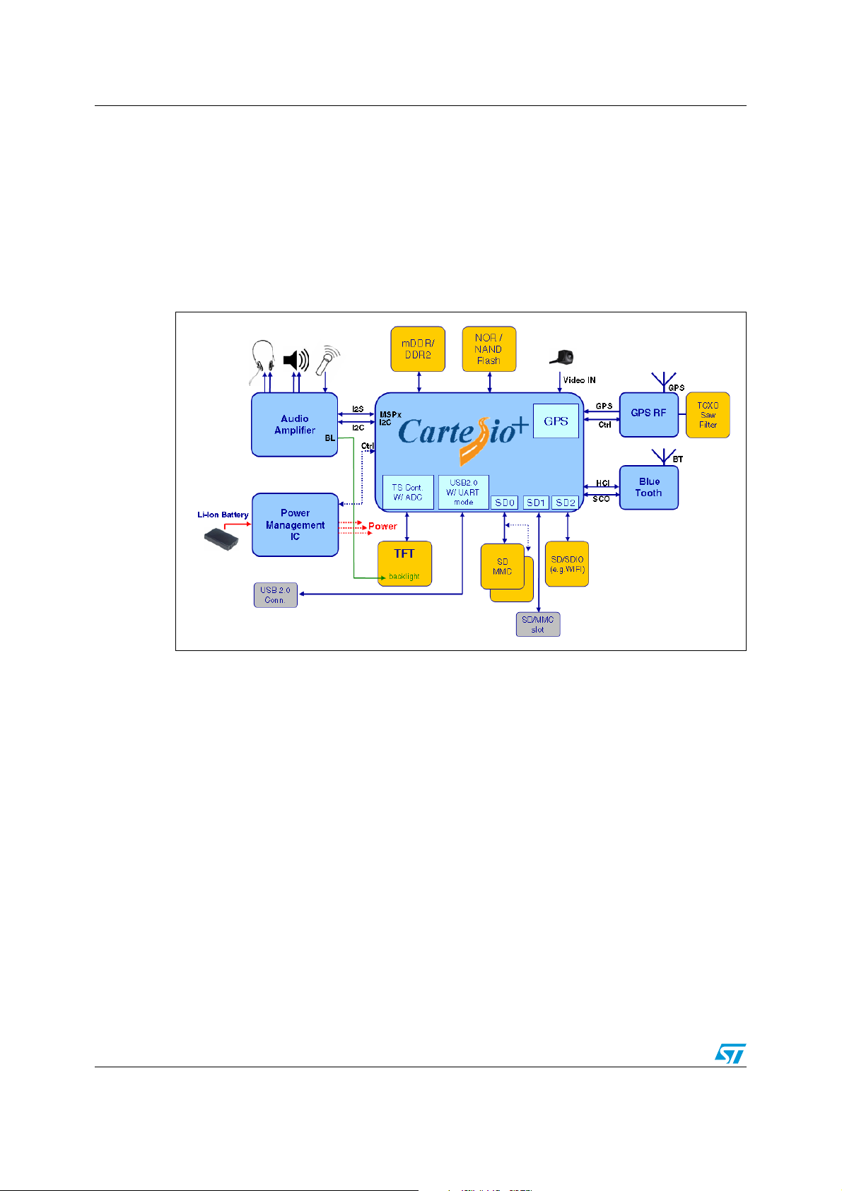
Figure 1. Application implementation example
4/19 Doc ID 16057 Rev 3
Page 5

STA2064 System description
2 System description
2.1 MCU
ARM1176-JZF advanced risc machine CPU up to 533 MHz (with Vdd greater or equal to
1.20 V and under process and temperature worst case conditions).
2.2 Embedded memories
2.2.1 Embedded SRAM (eSRAM)
The embedded SRAM is 8K x 32 (32 KB).
2.3 System functions
2.3.1 System and reset controller (SRC)
This provides a control interface for clock generation components external to the subsystem.
It also controls system-wide and peripherals-specific energy management features.
2.3.2 PMU
The power manager module controls the SLEEP to DEEP-SLEEP modes transition,
controls the external voltage switches on the Vdd and Vddio, monitors the external power
supply (via two signals, Vddok and BATOK), can force the emergency entry of the SDRAM
in self-refresh, and controls the wake-up from DEEP-SLEEP mode.
2.3.3 DMA
Direct memory access can be used with DMA peripherals. FIFO fill/empty requests from
these peripherals can be serviced immediately by the DMA Controller without CPU
interaction. Peripheral-to-peripheral and memory-to-memory DMA are also supported.
STA2064 features two DMA engines. Each DMA supports up to 8-channels and up to 32
requests.
2.3.4 Vectored interrupt controller (VIC)
The VIC allows the OS interrupt handler to quickly dispatch interrupt service routines in
response to peripheral interrupts.
2.3.5 GPIOs
Four GPIO ports provide 65 programmable inputs or outputs that can be controlled in two
modes:
● software mode through an APB bus interface
● hardware mode through a hardware control interface
Doc ID 16057 Rev 3 5/19
Page 6

System description STA2064
2.3.6 Real-time clock (RTC)
The RTC provides a one second resolution clock. This keeps time when the system is
inactive and can be used to wake the system up when a programmed ‘alarm’ time is
reached. It has a clock trimming feature to compensate the drift of the 32.768 kHz crystal.
2.3.7 Real-time timer (RTT)
The RTT has the possibility of being clocked off. This reduces the always_on domain
consumption during Deep Sleep. By default the RTT has its clock enabled.
2.3.8 Always_ON supply
The “Always_ON” domain retains its two separate supplies, one for the core logic (V
and one for the IOs (V
The V
supply is equal to VDD during normal operation but, with the goal of reaching the
DDON
IOON
).
lowest consumption possible, can also be configured as low as 1.0 ±10%V when the device
is in deep-sleep.
2.3.9 Enhanced function timer (EFT)
STA2064 features 4 16-bit EFTs. Each of the four EFT timers has a 16-bit free-running
counter with 7-bit prescaler, up to two input capture/output compare functions, a pulse
counter function, and a PWM channel with selectable frequency.
2.3.10 Watchdog timer (WDT)
This OS resource is used to trigger a system reset in the event of software failure.
2.4 Memory interfaces
2.4.1 SD/MMC
STA2064 features two SD/SDIO/MMC interfaces up to 52 MHz / one up to 8-bit data, the
other up to 4-bit data. The main clock available to the peripherals is:
● PLL2CLK/13 (when PLL2CLK is 624 MHz and SRC_MMC52 = 0, 48 MHz will be
generated)
● PLL2CLK/12 (when PLL2CLK is 624 MHz and SRC_MMC = 1, 52 MHz will be
generated)
● PLL2CLK/9 (when PLL2CLK is 432 MHz, 48 MHz will be generated)
DDON
)
The peripheral is compliant to the following standards:
● MMC 4.4
● SD 2.0/Part 1 - Physical Layer
● SD 2.0/Part E1 - SDIO Specification
6/19 Doc ID 16057 Rev 3
Page 7

STA2064 System description
2.4.2 DDR-SDRAM controller
The SDRAM controller has been designed to support up to 1Gbit over each of the two chip
selects (or up to 2 Gbit over a single chip select) of:
● LP DDR-SDRAM
● DDR2
The memory data bus will be 16 or 32-bit wide for LP DDR-SDRAM memories (under
software control). This same configuration is also supported for DDR2 type of memories,
with two 16-bit devices per chip select.
2.5 Audio/video functions
2.5.1 C3
It is composed of CD-ROM Decoder Block, responsible for performing sector descrambling
rd
and 3
Form1, and Data Filter block supporting frame data filtering and different block layout
organization possibilities. The C3 block can take its input data directly from SPDIF or from
the memory space, and delivers back its output data to memory, supporting DMA requests.
level of error correction embedded in the sector specific to CD-ROM mode1 and XA
2.5.2 Sample rate converter (SaRaC)
This block offers a fully digital stereo asynchronous sample rate conversion, using an
automatic Digital Ratio Locked Loop. Its main features are:
– Up to 20-bit input and 22-bit output sample size
– DMA optimized 16-bit stereo sample interface
– Input sample rate from selectable MSP or SPDIF interface (32 kHz to 48 kHz)
– Output sample rate from selectable MSP interface (44.1 kHz to 48 kHz)
– Internally generated input sample rate (8 kHz to 48 kHz) for compressed audio
decoding
2.5.3 JPEG decoder
The JPEG decoder block performs Baseline DCT sequential decoding up to 16Mpix/sec.
JPEG compressed thumbnails are also supported.
2.5.4 Smart graphic accelerator (SGA)
The smart graphic accelerator (SGA) provides an efficient 2D and 3D primitive drawing tool
that breaks down the MIPS and power consumption concerns of pixel processing.
2.5.5 Color LCD controller (CLCD)
This interface drives LCD panels. It supports single or dual-panel color and monochrome
STN displays and color TFT or HR-TFT displays. The resolution can be 1, 2 or 4 bitsperpixel (bpp) palletized for mono STN, 1, 2, 4 or 8 bpp palletized for color STN and TFT,
16-bpp true-color non palletized for Color STN and TFT, 18-bpp packed or not packed
truecolor non pallettized for color TFT. It also offers Frame Modulation to deliver enhanced
colors on 12, 16 or 18 bits (HR-) TFT panels from up to 18-bpp format.
Doc ID 16057 Rev 3 7/19
Page 8

System description STA2064
2.6 Communication interfaces
2.6.1 USB
STA2064 embeds one USB2.0 OTG high-speed interface, featuring:
a) High-speed signalling rate at 480 Mbit/s
b) Support for full-speed (12 Mbit/s) signaling bit rate
c) Support for session request protocol (SRP) and host negotiation protocol (HNP)
d) Up to 7 bidirectional endpoints plus control endpoint 0
e) 8192 bytes maximum FIFO dimension
f) Dynamic FIFO allocation
To reduce total system cost, it is equipped with a built-in USB 2.0 PHY.
With the goal of reducing the BOM cost for the customer, the USB 2.0 PHY also supports
this additional muxing scheme:
● the USB D- wire is used as either the USB D- signal or UART receive data signal
● the USB D+ wire is used as either the USB D+ signal or the UART transmit data signal
2.6.2 UART
STA2064 features four Autobaud UARTs. One offers all modem control/status signals. They
are enhanced version of the industry-standard 16C550 UART.
2.6.3 I2C
The I2C controller is an interface designed to support the physical and data link layer
according to I
that provides a low-cost interconnection between ICs. STA2064 features three I
interfaces.
2.6.4 MSP
The multichannel serial port (MSP) is a synchronous receive and transmit serial interface.
STA2064 features three MSPs.
2.6.5 SSP
STA2064 features two SSPs up to 24Mbit/sec for synchronous serial communication with
external peripherals. SPI, MicroWire, T.I. and mono-directional protocols are supported with
programmable word length up to 32 bits.
2.6.6 SPDIF
This interface takes SPDIF as input and extracts data and other channel information
encrypted in SPDIF Frame format as per IEC958 standards. Data can be transferred to
memory, using DMA support, or directly to C3 decoder without CPU intervent. SPDIF block
supports up to 2X data streams.
2
C standard revision 2.1 (January 2000). The I2C bus is a 2-wire serial bus
2
C
8/19 Doc ID 16057 Rev 3
Page 9

STA2064 System description
2.6.7 AC97 controller
AC97 audio controller enables SOC to control external AC97 CODECs using SOC AMBA
interconnect. It is implemented in a way to minimize audio data handling by SOC processor
with dedicated audio DMA engine. AC97 Audio Controller supports AC97 revision 2.3
compliant audio CODECs. External interface supports one external AC97 CODEC with 6
output (3 of them can be Double Rate Audio) and 3 input channels.
2.6.8 CAN
STA2064 features one CAN module that is compliant with the CAN specification V2.0 part B
(active). The bit rate can be programmed up to 1 MBaud.
2.7 Specific functions
2.7.1 GPS
STA2064 integrates HPGPS_G2, ST’s proprietary GPS IP, which is ST’s 2nd generation
High-Sensitivity Baseband. The Baseband is fully compliant with GPS and Galileo L1/E1
signal specifications, and is optimised to maximise sensitivity for both acquisition and
tracking in difficult environments. Please refer to GPS solution specifications and software
release notes for more specific performance details.
The baseband accepts a 3-bit signal at a 4MHz IF from its companion RF chip, the
STA5630. It downconverts this to baseband and feeds it to the acquisition engines (for up to
8 satellites simultaneously) and the tracking channels (for up to 32 satellites
simultaneously).
The highly parallel correlators in the acquisition engines identify each satellite signal in time
and frequency domains, and the results are passed to the tracking channels. The tracking
channels fine-tune the lock, then track continuously, providing orbit data and timing
measurements to the ARM CPUs.
The management of the hardware for these operations, and the myriad of complex
conditions that arise, is performed in a complete GPS software library supplied by ST. This
library also takes the resultant measurement data and processes it to maintain satellite
databases and calculate the user's position, velocity and time(PVT) solutions.
The PVT solution, and other useful data, is made available to the user's application via an
API in the ST GPS library. This runs on a royalty-free real-time kernel (OS20), with ports to
industry-standard operating systems also available. In stand-alone mode, the outputs are
generated in standard NMEA message format.
Options are also available in the software library to support ST Self-Trained Assisted GPS
(ST-AGPS), a complete and scalable solution for assisting GPS start-up with Autonomous
Ephemeris prediction when no network is available, and with simple download when a
network is available followed by prediction for the following 7 days.
The GPS subsystem is based on an ARM966 processor and is clocked by two clocks:
● MCLK: ARM966 CPU clock
● RFCLK: 16f
MCLK is derived from the PLL2 clock with a divisor from 3 to 16, giving an ARM966
operating frequency in the range from 208 to 39 MHz, in the case the PLL2 is running at 624
or 32f0, from RF chip
0
Doc ID 16057 Rev 3 9/19
Page 10

System description STA2064
MHz. The same divisor will be from 2 to 16 when the PLL2 is running at 432 MHz, giving an
operating frequency in the range from 216 to 27 MHz.
The GPS baseband clock will be derived from the MCLK clock with a divider, internal to the
subsytem, by 1, 2,3 or 4, under ARM11 control. RFCLK is the clock received from the RF
front-end chip.
2.7.2 Touchscreen controller/ADC
STA2064 embeds a 4-wire Touch Screen Controller. The Touch Screen Controller main
characteristics are:
● Active Window Clip
● Movements Tracking
● 12-bit SAR ADC resolution when used for Touch screen (with averaging)
● Measurement oversampling from 2 to 8
● Up to 128 coordinates FIFO, with programmable FIFO threshold
● ADC minimum conversion time of 1 μs
● Capability to support 4 additional analog inputs for auxiliary functions like battery
voltage monitoring and accessory control.
The ADC of the Touch Screen Controller can be also used for the conversion of external
analog signals. In this case the ADC has a 10-bit resolution (its native resolution).
2.7.3 Multisupply IO ring
STA2064 has multivoltage IOs capable of supporting 1.8V, 2.5V or 3.3V interfaces. The
rings are defined as follows:
● A: All peripherals with exception of what belongs to other rings
● B: LCD
● C: DRAM
● E: MMC1 (GPIO40-47, GPIO76-82), CAN0
The default voltage applied to each ring will be at reset time will be:
● A: 1.8V
● B: 1.8V
● C: 1.8V
● E: 3.3V
The “Always ON” ring remains separated as in the current STA2064 and supplied by V
IOON
.
10/19 Doc ID 16057 Rev 3
Page 11

STA2064 System description
2.7.4 Driving strength and slew rate programmability
The IO Driving Strength is programmable for the following interfaces as follows:
● SD/MMC0 (4, 6, 8 mA) (default 8mA)
● SD/MMC1 (4, 6, 8 mA) (default 8mA)
● LCD (4, 8 mA) (default 8mA)
● DRAM (weak 70Ω, strong 50Ω) (default strong, 50Ω)
The Slew Rate is also controllable for the following interface as follows:
● SD/MMC0 (Nominal, Fast) (default Nominal slew rate)
● SD/MMC1 (Nominal, Fast) (default Nominal slew rate)
● LCD (Nominal, Fast) (default Fast slew rate)
● DRAM (200, 266, 333 MHz) (default 200 MHz)
● MSP0 (Nominal, Fast) (default Nominal slew rate)
● MSP1 (Nominal, Fast) (default Nominal slew rate)
Doc ID 16057 Rev 3 11/19
Page 12

System features introduction STA2064
3 System features introduction
In this chapter, an introduction to the main STA2064 system features is given. These will be
explained in detail later in this document.
3.1 Power region partition
STA2064 is a device targeted to wide range of applications, starting from handheld battery
powered devices thanks to an optimzed power management but also addressing in dash
automotive power requirements thanks to its flexibile multivoltage IO.
Three main power regions are identified:
● V
● V
● V
: It is the core voltage that powers the RTC (real-time clock), the PMU (Power
dd_on
Management Unit), SRC (System Clock and Reset controller) and the Backup RAM of
STA2064. V
remains usually powered even when the device is in DEEP-SLEEP
dd_on
mode. For this reason, the static power consumption of this region stays below 20uA
worst case.
: It is the core voltage that powers the overall chip (apart from the IOs). This voltage
dd
is not applied in very low power state condition. When applied, the V
and Vdd are
dd_on
at the same voltage. A maximum of 10% variation between the two regions is required.
: It is the power region dedicated to the IOs. The overall IOs are divided in seven
ddio
groups and each of them can be powered at different, independent voltages. Some
groups may have specific constraint in terms of power voltage range in order to meet
specific electrical characteristic compliant to some standards; some of these groups
are, for example, in the DDR interface and the 1.1 embedded USB transceiver. There is
also a group of IOs called V
that identifies the IOs that must be always powered
ddio_on
(also in the lowest power consumption state of STA2064) in order to make the wake-up
possible. The other five regions (called also V
) can not be powered while in this
ddiox
state. For more information, please refer to Chapter 3.6: IO groups on page 16.
3.2 Frequency region partition
STA2064 is designed so that there are two PLLs. PLL1 generates clock frequencies for the
ARM core and the internal buses, while the PLL2 generates clock frequencies for each
peripheral kernel and also for each peripheral interface. This means that each peripheral
receives the clock derived from the PLL1 at its internal interface, then it works with the clock
derived from the PLL2. Despite the use of two PLLs, a single system clock input or a single
external crystal is needed (in addition to the RTC clock (or crystal)).
12/19 Doc ID 16057 Rev 3
Page 13

STA2064 System features introduction
3.3 Frequency and power range
The core voltage range is 1.25 ±4 %V while the IO voltage ranges are 1.8 ±10 %V,
2.5 ± 10 %V and 3.3 ± 10 %V.
Ta bl e 2 shows some use cases of STA2064 in NORMAL mode:
Table 2. Frequency and power use cases
Vdd and V
1.2 5(±4%) 533 177.67 177.67 S
1.2 5(±4%) 533 133.25 133.25 S
1.2 5(±4%) 533 177.67 312 A, DDR2
1.2 5(±4%) 520 208 130 A
1.2 5(±4%) 520 173.34 173.34 S
1.2 5(±4%) 520 130 130 S
1.2 5(±4%) 520 208 312 A, DDR2
1.2 5(±4%) 494 197.6 197.6 S
1.2 5(±4%) 494 164.67 164.67 S
1.2 5(±4%) 494 123.5 123.5 S
1.2 5(±4%) 494 208 329.34 A, DDR2
dd_on
(V)
Core Freq
[MHz]
Bus Freq
[MHz]
DDR Freq
[MHz]
Sync/Async
[S/A]
The background of Tab l e 2 is the maximization of data throughput on the DRAM interface,
matching the currently available DRAM speed grades: 133 MHz, 166 MHz and 200 MHz (LP
DDR) and 333 MHz (DDR2). Despite this, it is possible to program the ARM core, the
internal bus and the DDR to run at different speeds than the ones mentioned in Ta bl e 2 The
ARM bus clock and the bus clock are derived from the same common source (VCO of the
PLL1) but are asynchronous each other. The DDR frequency can be the same
(synchronous) or derived with a different prescaling (1,2,3,4,5,6,8,9 or 10) from the VCO of
PLL1 or PLL2 (asynchronous configuration).
STA2064 embeds a complete GPS subsystem where both gate logic and dedicated DSP
work together. There are specific constraints in this subsystem in terms of minimum
frequency in order to guarantee the target GPS specifications.
In the lowest power consumption state as possible, only V
is powered and the target
dd_on
current drawn is 20 μA. In this state, the clock is not running and the current leakage is
mainly due to the Backup memory. The 20 μA current limit has to be considered with
Process best (leakage worst case condition), V
Junction Temperature 50
o
C (considering, while in this state, the ambient temperature is
1.3V (1.25V plus 4% tolerance) and
dd_on
equal to the junction temperature).
Doc ID 16057 Rev 3 13/19
Page 14

System features introduction STA2064
3.4 Power states
The following power states are defined:
● OFF: V
retention is kept in the SDRAM
● NORMAL: Each peripheral runs at its nominal speed with the possibility of turning off
all the unused peripherals (peripheral kernel clock gated)
● SLOW: PLL1 bypassed. ARM and bus runs at crystal clock. PLL2 runs at its nominal
speed. PLL1 can be optionally put in power down
● DOZE: It is like SLOW mode with the ARM running either at 19 MHz or 32 kHz
● STANDBY: PLLs run at their nominal speed. Clocks are gated, ARM in WFI (Wait For
Interrupt) state
● DEEP-SLEEP: V
clocked at 32 kHz making the wakeup possible. The context is put in the external
SDRAM while in self refresh mode. Only the V
● SLEEP: It is like the DEEP-SLEEP mode, with the difference that V
also applied and all the PLLs are off (optional for PLL2)
● BACKUP: It is like DEEP-SLEEP, with the difference that the context is not saved in the
external SDRAM. When coming out from Backup to any power state, the ARM core will
execute the first code instruction after 2ms from power on reset release.
and Vdd are not applied (all data in the backup RAM is lost): no data
dd_on
powered off. V
dd
powered (RTC, few GPIOs, backup RAM) and
dd_on
region must be powered
ddio_on
dd
and V
ddio
are
While in NORMAL, SLOW AND STANDBY, V
and Vdd are the same (10% tolerance
dd_on
between them) and cannot be changed. Also the power to the several IO groups is kept
unchanged.
In order to change the V
dd_on
and V
values, the system has to transit to either OFF,
dd
SLEEP, DEEP-SLEEP or BACKUP and then back to the selected state.
In order to keep the power consumption as low as possible, the target voltage mentioned in
DEEP-SLEEP is considered at 1.0V.
A dedicated FSM manages the power state transitions among NORMAL, SLOW, DOZE
AND SLEEP. All other states mentioned above are SW variants of the ones managed by the
FSM.
Ta bl e 3 shows the summary of the power states supported by STA2064.
Table 3. Power mode states
Power State 32 kHz PLL1 PLL2 V
NORMAL on on on 1.2V to 1.3V =V
SLOW on
DOZE on
STANDBY on
SLEEP on off
dd_on
OFF off off off off off off
Off. Bypassed by
main oscillator
Off. Bypassed by
32 kHz
on (clk gated)
ARM in WFI
off (SW can
take it on)
off (SW can
take it on)
1.2V to 1.3V =
1.2V to 1.3V =V
on (clk gated) 1.2V to 1.3V =V
off (SW can
take it on)
1.2V to 1.3V
(typically 1.25V)
V
dd_on
Vdd_on
=V
dd
dd_on
dd_on
dd_on
IOs
1.7 to 3.6V
1.7 to 3.6V
1.7 to 3.6V
1.7 to 3.6V
1.7 to 3.6V
14/19 Doc ID 16057 Rev 3
Page 15

STA2064 System features introduction
Table 3. Power mode states (continued)
Power State 32 kHz PLL1 PLL2 V
OFF off off off off off off
NORMAL on on on 1.2V to 1.3V =V
DEEP-SLEEP on off off
BACKUP on off off
dd_on
1.2V to 1.3V
(typically 1.25V)
1.2V to 1.3V
(typically 1.25V)
3.5 System wakeup and power down
Typically the system using STA2064 will never be powered off, even when the user switches
the device off using the main power switch. The main power switch works in a way that puts
the device either in Backup or in DEEP-SLEEP mode. In this state, the only blocks within
STA2064 that are powered are the RTC, PMU, PWL, SRC and the backup RAM; at system
level, only the V
The following wakeup methods are possible:
● The user presses a button on the unit that causes all of the main power supplies to
start. After an appropriate delay, the processor's reset line is lifted and allows the code
to start executing
● The internal alarm feature triggers a dedicated signal that will cause all of the main
supplies to start. After an appropriate delay, the processor's reset line is lifted and
allows the code to start execution
is powered.
dd_on
V
dd
dd_on
off
off
IOs
1.7 to 3.6V
Refer section
3.5
Refer section
3.5
Considering the above mentioned wakeup system, while in DEEP-SLEEP and in BACKUP
state also, some dedicated IO lines must be powered:
● POR (input)
● POWEREN (output)
● VDDOK and BATOK (input)
● WAKE (input)
● 32 kHz crystal (SXTALI and SXTALO)
● OSC32KOUT (output)
In order to keep the external DRAM in self refresh while in DEEP-SLEEP, CKE of the DRAM
must be kept low. Since all the IOs are not powered in DEEP-SLEEP, in order to make the
self refresh working, an external pulldown resistor is needed.
Doc ID 16057 Rev 3 15/19
Page 16

System features introduction STA2064
3.6 IO groups
V
is split into the following groups:
ddio
● V
ddio_on
V
●
ddiox
●
V
USB
The IO supply type and corresponding pads details are as follows:
● V
ddio_on
POR, PWREN, VDDOK, BATOK, WAKE, SXTALI, SXTALO, OSC32KOUT
● V
ddioA
pads for JTAG, MMC0 and GPS
● V
ddioB
● V
ddioC
● V
ddioD
GPIO96:127 and dedicated pads for TEST (SCANEN, TAPSEL)
● V
ddioE
GPIOs related to SDMMC functionality
● V
USB
● V
TSC
(a)
(This is split into 5 types: V
ddioA
, V
ddioB
, V
ddioC
, V
ddioD
, V
ddioE
(b)
)
(USB 2.0 PHY transceiver)
: Power Supply pins for the IO buffers of the always ON section. It supplies
: Power Supply pins for the IO buffers. It supplies most GPIOs and dedicated
: Power Supply pins for the IO buffers. Supplies to the CLCD IOs
: Power Supply pins for the IO buffers. Supplies the SDMC IOs
: Power Supply pins for the IO buffers. Supplies the following IOs: GPIO64:67,
: Power Supply pins for the IO buffers. Supplies the following IOs: CAN, MSP,
: 3.3V USB PAD power supply
: 3.3V Touchscreen PAD power supply.
a. Vddio_on is always 1.8V.
b. When V
powered with same voltage level i.e 2.5V. V
vice-versa is not true. So for example, application can power voltage bank B with 2.5V (keeping its PSW=1)
and V
domain A is powered with 2.5V (its PSW bit = 1), all other V
ddio
A as 1.8V.
ddio
domain C and V
ddio
16/19 Doc ID 16057 Rev 3
ddio
ddio_coreon
domains (B, D, E) should be
is always powered with 1.8V. The
Page 17

STA2064 Package information
4 Package information
In order to meet environmental requirements, ST offers these devices in different grades of
ECOPACK
®
packages, depending on their level of environmental compliance. ECOPACK
®
specifications, grade definitions and product status are available at: www.st.com.
ECOPACK
®
is an ST trademark.
Figure 2. TFBGA289 (15x15x1.2mm) mechanical data and package dimensions
DIM.
A 1.200 0.0472
A1 0.250 0.0098
A2 0.200 0.0079
A4 0.585 0.0230
b 0.350 0.400 0.480 0.0138 0.0157 0.0189
D 14.850 15.000 15.150 0.5846 0.5906 0.5965
D1 12.800 0.5039
E 14.850 15.000 15.150 0.5846 0.5906 0.5965
E1 12.800 0.5039
e 0.800 0.0315
Z 1.100 0.0433
ddd 0.120 0.0047
eee 0.150 0.0059
fff 0.080 0.0031
mm inch
MIN. TYP. MAX. MIN. TYP. MAX.
OUTLINE AND
MECHANICAL DATA
Body: 15 x 15 x 1.2mm, pitch 0.8mm
TFBGA289
Thin profile Fine Pitch Ball Grid Array
8177030 A
Doc ID 16057 Rev 3 17/19
Page 18

Revision history STA2064
5 Revision history
Table 4. Document revision history
Date Revision Changes
22-Jul-2009 1 Initial release.
13-Oct-2009 2 Updated features list on page 1.
19-Oct-2009 3
Updated “Standard interfaces” feature on cover page.
Updated Section 2.6.2: UART on page 8.
18/19 Doc ID 16057 Rev 3
Page 19

STA2064
Please Read Carefully:
Information in this document is provided solely in connection with ST products. STMicroelectronics NV and its subsidiaries (“ST”) reserve the
right to make changes, corrections, modifications or improvements, to this document, and the products and services described herein at any
time, without notice.
All ST products are sold pursuant to ST’s terms and conditions of sale.
Purchasers are solely responsible for the choice, selection and use of the ST products and services described herein, and ST assumes no
liability whatsoever relating to the choice, selection or use of the ST products and services described herein.
No license, express or implied, by estoppel or otherwise, to any intellectual property rights is granted under this document. If any part of this
document refers to any third party products or services it shall not be deemed a license grant by ST for the use of such third party products
or services, or any intellectual property contained therein or considered as a warranty covering the use in any manner whatsoever of such
third party products or services or any intellectual property contained therein.
UNLESS OTHERWISE SET FORTH IN ST’S TERMS AND CONDITIONS OF SALE ST DISCLAIMS ANY EXPRESS OR IMPLIED
WARRANTY WITH RESPECT TO THE USE AND/OR SALE OF ST PRODUCTS INCLUDING WITHOUT LIMITATION IMPLIED
WARRANTIES OF MERCHANTABILITY, FITNESS FOR A PARTICULAR PURPOSE (AND THEIR EQUIVALENTS UNDER THE LAWS
OF ANY JURISDICTION), OR INFRINGEMENT OF ANY PATENT, COPYRIGHT OR OTHER INTELLECTUAL PROPERTY RIGHT.
UNLESS EXPRESSLY APPROVED IN WRITING BY AN AUTHORIZED ST REPRESENTATIVE, ST PRODUCTS ARE NOT
RECOMMENDED, AUTHORIZED OR WARRANTED FOR USE IN MILITARY, AIR CRAFT, SPACE, LIFE SAVING, OR LIFE SUSTAINING
APPLICATIONS, NOR IN PRODUCTS OR SYSTEMS WHERE FAILURE OR MALFUNCTION MAY RESULT IN PERSONAL INJURY,
DEATH, OR SEVERE PROPERTY OR ENVIRONMENTAL DAMAGE. ST PRODUCTS WHICH ARE NOT SPECIFIED AS "AUTOMOTIVE
GRADE" MAY ONLY BE USED IN AUTOMOTIVE APPLICATIONS AT USER’S OWN RISK.
Resale of ST products with provisions different from the statements and/or technical features set forth in this document shall immediately void
any warranty granted by ST for the ST product or service described herein and shall not create or extend in any manner whatsoever, any
liability of ST.
ST and the ST logo are trademarks or registered trademarks of ST in various countries.
Information in this document supersedes and replaces all information previously supplied.
The ST logo is a registered trademark of STMicroelectronics. All other names are the property of their respective owners.
© 2009 STMicroelectronics - All rights reserved
STMicroelectronics group of companies
Australia - Belgium - Brazil - Canada - China - Czech Republic - Finland - France - Germany - Hong Kong - India - Israel - Italy - Japan -
Malaysia - Malta - Morocco - Philippines - Singapore - Spain - Sweden - Switzerland - United Kingdom - United States of America
www.st.com
Doc ID 16057 Rev 3 19/19
 Loading...