

Page 1

96kHz DIGITAL AUDIO INTERFACE TRANSMITTER
MONOLITHIC DIGITAL AUDIO INTERFACE
TRANSMITTER
3.3V SUPPLYVOLTAGE
SUPPORTS:
- AES/EBU,IEC 958,
- S/PDIF,& EIAJCP-340
- Professionaland Consumer Formats
PARITYBITSAND CRCCODESGENERATED
TRANSPARENT MODE ALLOWS DIRECT
CONNECTIONOF STA020 AND STA120
STA020
PRODUCT PREVIEW
SDIP24 SO24
DESCRIPTION
The STA020 is a monolithic CMOS device which
encodes and transmits audio data according to
the AES/EBU, IEC 958, S/PDIF, & EIAJ CP-340
interface standards. It supports 96kHz sample
rate operation
The STA020 accepts audio and digital data which
is then multiplexed, encoded and driven onto a
cable.
The audio serial port is double buffered and ca-
BLOCK DIAGRAM
VD+
7
SCK
FSYNC
SDATA
M0 M1 M2 MCK RST
212223
6
7
8
10
C
11
U
9
V
AUDIO
SERIAL PORT
REGISTERS
ORDERING NUMBERS:
STA020 STA020D
pable of supportinga wide variety of formats.
The STA020 multiplexes the channel, user, and
validity data directly from serial input pins with
dedicated input pins for the most important channel statusbits.
GND
19
18
MUX DIFFERENTIAL
165
20
17
TXP
TXN
15 24
DEDICATED CHANNEL
STATUS BUS
October 1999
This is preliminaryinformation on a new product now in development. Details are subjectto change without notice.
CBL TRNPT
D97AU599A
1/12
Page 2
STA020
ABSOLUTE MAXIMUM RATINGS
Symbol Parameter Value Unit
V
D+
V
IND
T
amb
T
stg
RECOMMNDED OPERATINGCONDITIONS(GND = 0V; all voltageswith respect to ground)
Symbol Parameter Test Condition Min. Typ. Max. Unit
V
D+
T
amb
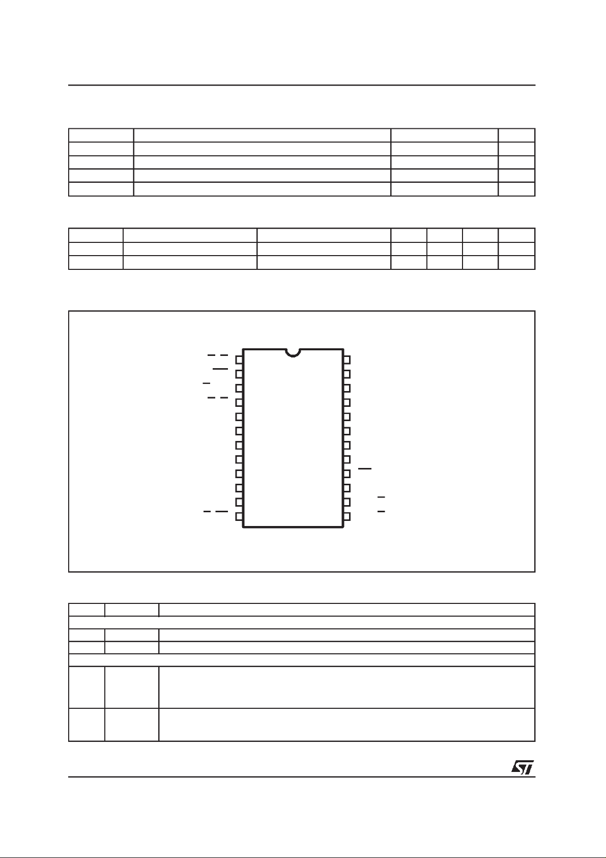
PIN CONNECTION
DC Power Supply 4 V
Digital Input Voltage -0.3 to VD+0.3 V
Ambient Operating Temperature (power applied) -20 to +85 °C
Storage Temperature -40 to 150 °C
DC Voltage 3 3.3 3.6 V
Ambient Operating Temp. 0 25 70 °C
C7/C3
PRO
C1/FC0
C6/C2
MCK TXP
SCK
FSYNC
SDATA
C/SBF
C9/C15
1
2
3
4
5
6
7
8
V
9
10
U
11
12
D97AU608A
24
23
22
21
20
18
17
16
15
14
13
PINS DESCRIPTION
N. Name Function
Power Supply Connections
18 GND Ground.
19 VD+ Positive Digital Power. Nominally +3.3V.
Audio Input Interface
6 SCK Serial Clock.
7 FSYNC Frame Sync.
Serial clock for SDATA pinwhich can be configured (via the M0, M1 and M2 pins) as an input
or output and can sample data on the rising or falling edge.As an output, SCK will contain 32
clocks for everyaudio sample.
Delineates the serial data andmay indicate the particular channel, left or right and may be an
input or output. The format is based on M0, M1 and M2 pins.
TRNPT/FC1
M0
M1
M2
VD+19
GND
TXN
RST
CBL/SBC
EM0/C9
EM1/C8
2/12
Page 3

PINS DESCRIPTION(continued)
N. Name Function
8 SDATA Serial Data.
21,
22,23
Control Pins
Transmitter Interface
20, 17 TXP, TXN Differential Line Drivers.
M0, M1, M2 Serial Port Mode Select.
1 C7/C3 Channel Status Bit 7/Channel Status Bit 3.
2 PRO Professional/Consumer Select.
3 C1/FC0 Channel Status Bit 1/Frequency Control 0.
4 C6/C2 Channel Status Bit 6/Channel Status Bit 2.
9 V Validity.
10 C/SBF Channel Status Serial Input/Subcode Frame Clock.
11 U User Bit.
12 C9/C15 Channel Status Bit 9/ChannelStatus Bit 15.
13 EM1/C8 Emphasis 1/Channel Status Bit 8.
14 EM0/C9 Emphasis 0/Channel Status Bit 9.
15 CBL/SBC Channel Status Block Output/Subcode Bit Clock.
16 RST Master Reset.
24 TRNPT/FC1 Transparent Mode/Frequency Control 1.
5 MCK Master Clock. Clock input at 128xthe sample frequency which definesthe transmit timing. In
Audio data serial input pin.
Selects the format of FSYNC and the sample edge of SCK withrespect to SDATA.
In professional mode, C7 is the inverse of channel status bit 7. In consumer mode, C3 is the
inverse of channel status bit 3, C7/C3 are ignored in Transparent Mode.
Selects between professional mode (PRO low) and consumer mode(PRO high). This pin
defines the functionality of the channelstatus parallel pins. PRO is ignored in Transparent
Mode.
In professional mode, C1 is the inverse of channel status bit 1. Inconsumer mode, FC0and
FC1 are encoded versions of channel status bits 24 and 25 (bits 0 and 1 of byte 3). When
FC0 and FC1 are both high, CD mode is selected. C1/FC0 are ignored in Transparent Mode.
In professional mode, C6 is the inverse of channel status bit 6. Inconsumer mode, C2 is the
inverse of channel status bit 2. C6/C2 are ignored in Transparent Mode.
Validity bit serial input port. This bitis defined as per the digital audio standards wherein V = 0
signifies the audio signal is suitable for conversion to analog. V = 1 signifiesthe audio signal is
not suitable for conversion to analog,i.e. invalid.
In professional and consumer modes this pin is the channel status serial input port. In CD
mode this pin inputs theCD subcode frame clock.
User bit serial input port.
In professional mode, C9 is the inverse of channel status bit 9 (bit 1 of byte 1). In consumer
mode, C15 is the inverse of channel status bit 15 (bit7 of byte 1). C9/C15 are ignored in
Transparent Mode.
In professional mode, EM0 and EM1 encode channelstatus bits2, 3 and 4. Inconsumer
mode, C8 is the inverse of channel status bit 8 (bit 0 of byte 1). EM1/C8 are ignored in
Transparent Mode.
In professional mode, EM0 and EM1 encode channelstatus bits2, 3 and 4. Inconsumer
mode, C9 is the inverse of channel status bit 9 (bit 1 of byte 1). EM0/C9 are ignored in
Transparent Mode.
In professional and consumer modes, the channel status block output is high for the first 15
bytes of channel status. In CD mode, this pin outputs the subcode bitclock.
When low, all internal counters are reset.
In professional mode, setting TRNPT low selects normal operation & CBL is an output. Setting
TRNPT high, allows the STA020 to be connected directly to an STA120. In transparent mode,
CBL is an input& MCK must be at 256Fs. In consumer mode, FC0 and FC1 are encoded
versions of channel status bits 24 and 25. When FC0 and FC1 are both high, CD mode is
selected.
trasparent mode MCK must be 256 Fs.
STA020
3/12
Page 4

STA020
DIGITAL CHARACTERISTICS (T
=25°C; VD+= 3.3V ±10%)
amb
Symbol Parameter Test Condition Min. Typ. Max. Unit
V
IH
V
IL
V
OH
V
OL
I
in
High-Level Input Voltage 2.0 VDD+0.3 V
Low-Level Input Voltage -0.3 +0.8 V
High-Level Output Voltage IO= 200µAV
-1.0 V
DD
Low-Level Output Voltage IO= 3.2mA 0.4 V
Input Leakage Current 1.0 10 µA
MCK Master Clock frequency (Note 1) 26 MHz
Master Clock Duty Cycle (high time/cycle time) 40 60 %
Note 1: MCKmust be 128x the input word rate, except in TransparentMode where MCK is 256x the inputword rate.
Figure 1. STA020 Professional& ConsumerModesTypical Connection Diagram.
AUDIO
DATA
PROCESSOR
µCONTROLLER
or
UNUSED
CHANNEL
STATUS BITS
CONTROL
FSYNC
SCK
SDATA
CBL
RST
EXTERNAL
CLOCK
MCK
5
7
6
8
15
C
10
U
V
STA020
11
9
16
8 DEDICATED C.S. BITS
+3.3V
19
VD+
18
24
23
22
21
20
17
GND
TRNPT
M0
M1
M2
TXP
TXN
0.1µF
SERIAL PORT
MODE SELECT
TRANSMITTER
CIRCUIT
D97AU600A
Figure 2. STA020 Typical ConnectionDiagram.
EXTERNAL
4/12
AUDIO
DATA
PROCESSOR
DECODER
SUBCODE
PORT
RESET
CONTROL
CHANNEL
STATUS BITS
CONTROL
FSYNC
SDATA
7
SCK
6
8
V
9
SBF
10
U
11
SBC
15
RST
16
8 DEDICATED C.S. BITS
CLOCK
5
STA020
MCK
+5V
19
VD+
0.1µF
GND
18
M0
23
M1
22
M2
21
TXP
20
TXN
17
SERIAL PORT
MODE SELECT
TRANSMITTER
CIRCUIT
See Appendix B
D99AU989A
Page 5

STA020
GENERAL DESCRIPTION
The STA020 is a monolithicCMOScircuit thatencodes and transmits audio and digital data according to the AES/EBU, IEC 958, S/PDIF, and
EIAJ CP-340 interface standards. The chip accepts audio and control data separately; multiplex
and biphase-mark encode the data internally and
drive it, directly or through a transformer, to a
transmissionline.
The STA020 has dedicated pins for the most important control bits and a serial input port for the
C, U and V bits.
Line Drivers
The differential line drivers for STA020 are low
skew, low impedance,differentialoutputs capable
of driving 110Ohm transmission lines. (RS422
line driver compatible).
They can also be disabled by resettingthe device
(RST = low).
STA020 DESCRIPTION
The STA020 accepts 16 to 24-bit audio samples
through a serial port configured in one of seven
formats; provides several pins dedicated to particular channel status bits and allows all channel
status, user and validity bits to be serially input
through port pins. This data is multiplexed, the
parity bit is generated and the bit stream is
biphase-mark encoded and driven through an
RS422 line driver.
The STA020 operates as a professional or consumer interface transmitter selectable by pin 2,
PRO. As a professional interface device, the
dedicated channel status input pins are defined
according to the professional standard, and the
CRC code (C.S. byte 23) can be internally generated.
As a consumer device, the dedicated channel
status input pins are defined according to the
consumer standard. A submode provided under
the consumermode is compact disk, CD, mode.
When transmitting data from a compact disk, the
CD subcode port can accept CD subcode data,
extract channel status information from it, and
transmit it as user data.
The master clock , MCK, controls timing for the
entire chip and must be 128xFs. As an example,
if stereo data is input to the STA020 at 44.1kHz,
MCK input must be 128 times that or 5.6448MHz.
Audio Serial Port
The audio serial port is used to enter audio data
and consists of three pins: SCK, SDATA and
FSYNC, SCK clocks in SDATA, which is double
buffered, while FSYNC delineates the audio samples and may indicate the particular channel,left
or right. To support many differentinterfaces,M2,
M1 and M0 select one of seven different formats
for the serial port. The coding is shown in Table 3
while the formats are shownin Figure3.
Format 0 and 1 are designed to interface with
Crystal ADCs. Format 2 communicates with Motorola and TI DSPs. Format3 is reserved.Format
4 is compatible with the I
2
S standard.Formats 5
and 6 make the STA020 look similar to existing
16- and 18-bit DACs and interpolation filters. Format 7 is an MSB-last format and is conducive to
serial arithmetic. SCK and FSYNC are outputs in
Format 0 and inputs in all other formats. In Format 2, the rising edge of FSYNC delineatessamples and the falling edge must occur a minimum
of one bit period before or after the risingedge.
In all formats except 2, FSYNC contains left/right
information requiring both edges of FSYNCto delineate samples. Formats 5 and 6 require a minimum of 16- or 18-bit audio words respectively. In
all formats other than 5 and 6, the STA020 can
accept any word length from 16 to 24 bits by adding leadingzeros in format 7 and trailing zeros in
the other formats, or by restricting the number of
SCK periods between active edges of FSYNC to
the sample word length.
FSYNC must be derived from MCK, either
through a DSP using the same clock or using
counters. If SFYNC moves (jitters) with respect to
MCK by four MCK periods, the internal counters
and CBLmay be reset.
Table 1. Audio Port Modes
M2 M1 M0 Format
0 0 0 0 - FSYNC & SCK Output
0 0 1 1 - Left/Right, 16-24 Bits
0 1 0 2 - Word Sync, 16-24Bits
0 1 1 3 - Reserved
1 0 0 4 - Left/Right, I
1 0 1 5 - LSB Justified, 16 Bits
1 1 0 6 - LSB Justified, 18 Bits
1 1 1 7 - MSB Last, 16-24 Bits
2
S Compatible
5/12
Page 6

STA020
Figure 3. Audio Serial Port Formats.
FORMAT 0:
FSYNC(out)
SCK(out)
SDATA(in)
FORMAT 1:
FSYNC(in)
SCK(in)
SDATA(in)
FORMAT 2:
FSYNC(in)
SCK(in)
SDATA(in)
FORMAT 3:
(RESERVED)
FORMAT 4:
FSYNC(in)
SCK(in)
SDATA(in)
FORMAT 5:
FSYNC(in)
SCK(in)
SDATA(in)
FORMAT 6:
FSYNC(in)
SCK(in)
SDATA(in)
FORMAT 7:
FSYNC(in)
SCK(in)
SDATA(in)
LSB MSB
LSB MSB
MSB LSB
LEFT RIGHT
MSB LSB MSB LSB MSB
LEFT RIGHT
MSB LSB MSB LSB MSB
LEFT RIGHT
MSB LSB MSB LSB MSB
LEFT RIGHT
MSB LSB MSB LSB MSB
LEFT RIGHT
LSB MSB LSB
16 Bits 16 Bits
LEFT RIGHT
LSB MSB LSB
18 Bits 18 Bits
LEFT RIGHT
MSB LSB MSB
D97AU604
C, U, V SerialPort
The serial input pins for channel status (C), user
(U), and validity (V) are sampled during the first
bit period after the active edge of FSYNC for all
formats except Format 4. Format 4 is sampled
during the second bit period (coincident with the
MSB). In Figure 3, the arrows on SCK indicate
when the C, U, and V bits are sampled. The C, U,
and V bits are transmitted with the audio sample
entered before FSYNC edge that sampled it. The
V bit, as defined in the audio standards, is set to
6/12
zero toindicate the audio data is suitable for conversion to analog. Therefore, when the audio
data is errored, or the data is not audio,the V bit
should be set high. The channel status serial input pin (C) is not available in consumer mode
when the CD subcode port is enabled (FC1 =
FC0 = high). Any channel status data entered
through the channel status serial input (C) is logically OR’ed with the data entered through the
dedicated pinsor internallygenerated.
Page 7

STA020
RST and CBL (TRNPT is low)
When RST goes low, the differential line drivers
are set to ground. In order to properly synchronize the ST020 to the audio serial port, the transmit timing counters, which include CBL, are not
enabled after RST goes high until eight and one
half SCK periods after reset is exited) of FSYNC.
When FSYNC is configured as a left/right signal
(all defined formats except 2), the counters and
CBL are not enabled until the right sample is being transmitted). This guarantees that channel A
is left and channel B is right as per the digital
audio interface specs.
As shown in Figure 4, channel block start output
(CBL), can assist in serially inputtingthe C, U and
V bits as CBL goes high one bit period before the
first bit of the preamble of the first sub-frame of
the channel status block is transmitted. This subframe contains channel status byte 0, bit 0. CBL
returns low one bit period before the start of the
frame that contains bit 0 of channel status byte
16. CBL is not available when the CD subcode
port is enabled.
Figure 4 illustrates timing for stereo data input on
the audio port. Notice how CBL rises while the
right channel data (Right 0) is input, but the previous left channel (Left 0) is being transmitted as
the first sub-frame of the channel status block
(starting with preamble Z). The C, U, and V input
ports only need to be valid for a shortperiod after
FSYNC changes. A sub-frame includes one
audio sample while a frame includes a stereo
pair. A channel status (C.S.) block contains 24
bytes of channel status and 384 audio samples
(or 192 stereo pairs, or frames, of samples).
Figure 4 shows the CUV ports as having left and
right bits (e.g. CUV0L, CUV0R). Since the C.S.
block is defined as 192 bits, or one bit per frame,
there are actually 2 C.S. blocks, one for channel
A (left) and one for channelB (right). When inputting stereo audio data, both blocks normally contain the same information, so C0L and C0R from
the input port pin are both channelstatus bit 0 of
byte 0, which is defined as professional/consumer. These first two bits from the port,C0L and
C0R, are logically OR’ed with the inverse PRO,
since PRO is a dedicated channel status pin defined as C.S. bit 0.
Also, if in professional mode, C1, C6, C7 and C9
are dedicatedC.S. pins. The inverseof C1is logically OR’ed with channel status input ports bits
C1L and C1R. In similar fashion, C6, C7 and C9
are OR’ed with their respective input bits. Also,
the C bits in CUV128L and CUV128R are both
channel status block bit 128, which is bit 0 of
channelstatusbyte 16.
Figure 4. CBL and TransmitterTiming.
TRNPT high
CBL
TRNPT low
SDATA
FSYNC
TRNPT high
C,U,V
TRNPT low
TXP
TXN
Preamble Y VUCP191R
LEFT 0 RIGHT 0 LEFT 1 LEFT 128 RIGHT 128 LEFT 0 RIGHT 0
C BITS FROM CPIN
CUV0L
CUV191R
OR’ed
C BITS
w/PRO pin
RIGHT 191 LEFT 0 RIGHT 0
CUV0R
CUV0L
VUCP0L
Preamble Z
bit
Preamble Z Aux Data LSB Left 0 - Audio Data MSB V0 U0 C0 P0
CUV1L
CUV0R
C BITS
OR’ed
w/C1 pin
VUCP0R
Preamble Y
SUB-FRAME
CUV1R
CUV1L
BITS 0 of
BLOCK BYTE16
LEFT
128
VUCP127R Preamble X
VUCP128L
CUV128R
CUV128L
RIGHT
Preamble Y
28 29 30 312783740
C.S.
128
CUV0L
CUV191R
D99AU990
CUV0R
CUV0L
7/12
Page 8

STA020
TransparentMode
In certain applicationsit is desirable to receivedigital audio data with the STA120 and retransmit it
with the STA020.In this case, channelstatus,user
and validity information must pass through unaltered. For studio environments,AES recommends
that signal timing synchronization be maintained
throughout the studio. Frame synchronization of
digital audio signals input to and output from a
pieceof equipmentmustbewithin +/-5%.
The transparent mode of the STA020is selected
by setting TRNPT, pin 24, high. In this mode, the
CBL pin becomes an input, allowing direct connection of the outputsof theSTA120 to the inputs
of the STA020 as shown in Figure 18. The transmitter and receiver are synchronized by the
FSYNC signal. CBL specifies the start of a new
channel status block boundry, allowing the transmit block structure to be slaved to the block structure of the receiver.
In the transparent mode, C, U and V are now
transmitted with the current audio sample as
shown in Figure 5 (TRNPT high) and the dedicated channelstatus pins are ignored.
When FSYNC is a word clock (Format 2), CBL is
sampled when left C, U, V are sampled. When
FSYNC is Left/Right, CBL is sampled when left
C, U, V are sampled. The channel status block
boundry is reset when CBL transitionsfrom low to
high (based on two successive samples of CBL).
MCK for the STA020 is normally expected to be
128 timesthe sample frequency, in the trasparent
mode MCK must be 256 Fs.
ProfessionalMode
Setting PRO low places the STA020 in professional mode as shown in Figure6. In professional
mode, channel status bit 0 is transmittedas a one
and bits 1, 2, 3, 4, 6, 7 and 9 can be controlled
via dedicated pins. The pins are actually the inverse of the identifiedbit.
For example, tying the C1 pin low places a one in
channel status bit 1. As shown in the application
Note, Overview of AES/EBU Digital Audio Interface Data Structures, C1 indicates audio/nonaudio; C6 and C7 determine the sample frequency and C9 allows the encoded channel
mode to be stereophonic. EM1 and EM0 determine emphasis and encode C2, C3, C4 as shown
in Table 2. Thededicated channelstatus pins are
read at the appropriate time and are logically
OR’edwith datainput onthechannelstatusport,C.
In Transparent Mode, these dedicated channel
status pins are ignored and channel status bits
are input at the C pin.
ConsumerMode
SettingPROhigh placesthe STA020in consumer
modewhichredefines the pins as shown in Figure
7. In consumermode, channelstatusbit 0 is transmittedas a zero and channel statusbits 2, 3, 8, 9,
15,24 and 25arecontrolledviadedicatedpins.
The pins are actually the inverse of the bit so if
pin C2 is tied high, channel status bit 2 will be
transmitted as a zero. Also, FC0 and FC1 are encoded versions of channel status bits 24 and 25,
which define the sample frequency.
When FC0 and FC1 are both high, the part is
placed in a CD submode which activates the CD
subcode port. This submodeis described in detail
in the next section. Table 3 describes the encoding of C24 and C25 through the FC1 and FC0
pins. According to AES/EBU standards, C2 is
copy prohibit/permit. C3 specifies pre-emphasis,
C8 and C9 define the category code and C15
identifies the generation status of the transmitted
material(i.e. first generation, secondgeneration).
Table 2. Emphasis Encoding
EM1 EM0 C2 C3 C4
00111
01110
10100
11000
Table 3. Sample Frequency Encoding
FC1 FC0 C24 C25 Comments
000044.1kHz
010148kHz
101132kHz
110044.1kHz, CD Mode
Figure 5. TransparentMode Interface.
V+
MCK
CBL
C
RXP
RXN SCK
STA120 STA020
U
V
FSYNC
SDATA
TRNPT
TXP
TXN
8/12
DATA
PROCESSING
D97AU605
Page 9

Figure 6. Block Diagram - Professional Mode
M0 M1 M2
23 22 21
SCK
8
6
7
10
C
11
U
V
REGISTERS
9
SERIAL
PORT
LOGIC
VALIDITY
PREAMBLE
SDATA
FSYNC
AUDIO
AUX
C Bits
CRC
U Bits
MUX
BIPHASE
MARK
ENCODER
TIMING
LINE
DRIVER
STA020
20
TXP
TXN
17
16
RST
MUX
2 14 13 3 4 1 12 15 5
PRO
EM0 EM1 C1 C6 C7 C9 CBL MCK
TRNPT
Figure 7. Block Diagram - Consumer Mode
M0 M1 M2
23 22 21
SCK
8
6
7
10
C
11
U
V
REGISTERS
9
SERIAL
PORT
LOGIC
SDATA
FSYNC
PARITY
24
AUDIO
AUX
C Bits
U Bits
VALIDITY
PREAMBLE
MUX
BIPHASE
MARK
ENCODER
TIMING
D97AU607B
LINE
DRIVER
20
TXP
TXN
17
16
RST
+3.3V
MUX
2
324 4 1131412 15 5
FC0 FC1 C2 C3 C8 C9 C15 CBL MCKPRO
PARITY
D97AU606A
9/12
Page 10

STA020
DIM.
MIN. TYP. MAX. MIN. TYP. MAX.
A 2.35 2.65 0.093 0.104
A1 0.10 0.30 0.004 0.012
A2 2.55 0.100
B 0.33 0.51 0.013 0.0200
C 0.23 0.32 0.009
D 15.20 15.60 0.598 0.614
E 7.40 7.60 0.291 0.299
e 1.27 0,050
H 10.0 10.65 0.394 0.419
h 0.25 0.75 0.010 0.030
k0°(min.), 8° (max.)
L 0.40 1.27 0.016 0.050
mm inch
0.013
OUTLINE AND
MECHANICAL DATA
SO24
0.10mm
.004
Seating Plane
1
A2
A
Be
A1
K
D
1324
E
12
hx45°
L
A1 C
H
SO24
10/12
Page 11

STA020
DIM.
mm inch
MIN. TYP. MAX. MIN. TYP. MAX.
A 5.08 0.20
A1 0.51
0.020
A2 3.05 3.30 4.57 0.120 0.130 0.180
B 0.36 0.46 0.56 0.0142 0.0181 0.0220
B1 0.76 1.02 1.14 0.030 0.040 0.045
c 0.23 0.25 0.38 0.009 0.0098 0.0150
D 22.61 22.86 23.11 0.890 0.90 0.910
E 7.62 8.64 0.30 0.340
E1 6.10 6.40 6.86 0.240 0.252 0.270
e 1.778 0.070
e1 7.62
0.30
e2 10.92 0.430
e3 1.52 0.060
L 2.54 3.30 3.81 0.10 0.130 0.150
OUTLINE AND
MECHANICAL DATA
SDIP24 (0.300”)
BeB1
D
24
1
13
12
A2
A1
Stand-off
F
SDIP24
E
E1
LA
e1
e2
c
E
.015
0,38
Gage Plane
e3
e2
11/12
Page 12

STA020
Information furnished is believed to be accurate and reliable. However, STMicroelectronics assumes no responsibility for the consequences
of use of such information nor for any infringement of patents or other rights of third parties which may result from its use. No license is
granted by implication or otherwise under any patent or patent rights of STMicroelectronics. Specification mentioned in this publication are
subject to change without notice. This publication supersedes and replaces all information previously supplied. STMicroelectronics products
are not authorizedfor use as critical components in lifesupport devices or systems without express written approval of STMicroelectronics.
The ST logois a registeredtrademark of STMicroelectronics
1999 STMicroelectronics – Printedin Italy – All Rights Reserved
STMicroelectronics GROUP OFCOMPANIES
Australia - Brazil - China- Finland - France - Germany - HongKong - India - Italy - Japan - Malaysia - Malta - Morocco -
Singapore - Spain - Sweden - Switzerland- UnitedKingdom - U.S.A.
http://www.st.com
12/12
 Loading...