

Page 1
®
STA014 STA014B STA014T
MPEG 2.5 LAYER III AUDIO DECODER WITH ADPC M AND
SRS WOW
The Device incorporates the SRS
WOW
cence from SRS Labs, Inc.
SINGLE CHIP MPEG2 LAYER 3 DECODER
SUPPORTING:
- All features specified for Layer III in ISO/IEC
11172-3 (MPEG 1 Audio)
- All features specified for Layer III in ISO/IEC
13818-3.2 (MPEG 2 Audio)
- Lower sampling frequencies syntax extension,
(not specified by ISO) called MPEG 2.5
DECODES LAYER III STEREO CHANNELS,
DUAL CHANNEL, SINGLE CHANNEL
(MONO)
SUPPORTING ALL THE MPEG 1 & 2 SAMPLING FREQUENCIES AND THE EXTENSION TO MPEG 2.5:
48, 44.1, 32, 24, 22.05, 16, 12, 11. 025, 8 KHz
ACCEPTS MPEG 2.5 LAYER III ELEMENTARY COMPRESSED BITSTREAM WITH
DATA RATE FROM 8 Kbit/s UP TO 320 Kbit/s
ADPCM CODEC CAPABILITIES:
- sample frequency from 8 kHz to 32 kHz
- sample size from 8 bits to 32 bits
- encoding al gor ith m: DV I,
ITU-G726 pack (G72 3-24, G72 1,G723-40)
- Tone control and fast-forward capability
SRS WOW
(1)
TECHNOLOGY CAN BE USED
AS POSTPROCESSING. SUPPORT FOR
DIFFERENT SPEAKERS TYPES:
- headphone
- medium
- large
(1)
WOW
TRUEBASS AND FOCUS CAN BE
INDIPENDENTLY ADJUSTED
EASY PRO GRAMMABL E GPSO I NTERF ACE
FOR ENCODED DATA UP TO 5Mbit/s
(TQFP44 & LFBGA 64)
DIGITAL VOLUME
BASS & TREBLE CONTROL
SERIAL BITSTREAM INPUT INTERFACE
EASY PRO GRAMMABLE ADC INPUT INTERFACE
ANCILLARY DATA E XTRACTION VI A I2C IN-
TERFAC E.
SERIAL PCM OUTPUT INTERFACE (I2S
AND OTHER FORMATS)
Technology under li-
POSTPROCESSING CAPABILITY
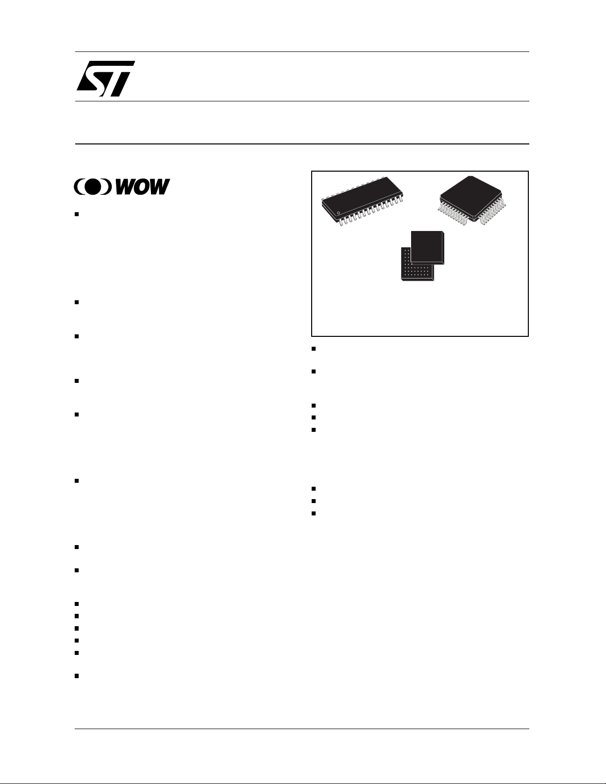
PRODUCT PREVIEW
ORDERING NUMBERS: STA014 (SO28)
STA014T (TQFP44)
STA014B (LFBGA 64)
PLL FOR INTERNAL CLOCK AND FOR OUT-
PUT PCM CLOCK GENERATION
CRC CHECK AND SYNCHRONISATION ER-
ROR DETECTION WITH SOFTWARE INDICATORS
I2C CONTROL BUS
LOW POWER 2.4V CMOS TECHNOLOGY
WIDE RANGE OF EXTERNAL CRYSTALS
FREQU ENCIES SUPPORTED
APPLICATIONS
PC SOUND CARDS
MULTIMEDIA PLAYERS
VOICE RECORDERS
DESCRIPTION
The STA014 is a fully integrated high flexibility
MPEG Layer III Audio Decoder, capable of decoding Layer III compressed elementary streams,
as specified in MPEG 1 and MPEG 2 ISO standards. The device decodes also elementary streams
compre s se d by using low sa m pling rat es, as specified by M PEG 2.5. ST A014 rece ives t h e inpu t dat a
throu gh a Seri al Inp ut Inter face. T he decode d signal is a stereo, mono, or dual channel digital output
that can b e sent di rectl y to a D/ A converter , by the
PCM Output Interface. This interface is software
programmable to adapt the STA014 digital output
to the most commo n DACs architectures used on
the market. The functional STA014 chip partitioning
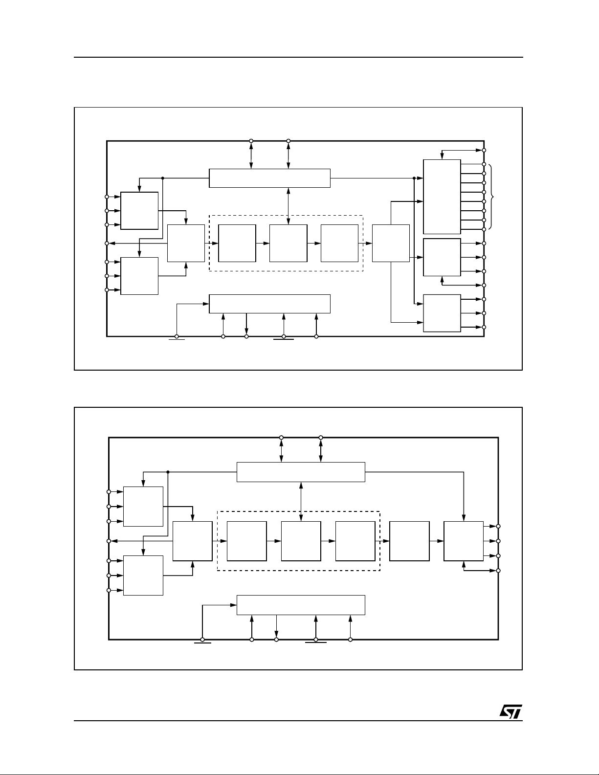
is described in Fig.1a and Fig.1b.
July 2000
This is preliminary information on a new product now in development or undergoing evaluation. Details are subject to change without notice.
(1)
in order to enable SRS WOW algorithm a mandatory configuration file is required.
1/45
Page 2
STA014-STA014B-STA014T
Figure 1a. BLOCK DIAGRAM for TQFP44 and LFBGA64 package
SDA SCL
31 32
TQFP44
I2C CONTROL
34
SDI
SCKR
BIT_EN
DATA-REQ
SCK_ADC
LRCK_ADC
SDI_ADC
36
38
27
40
26
24
SERIAL
INPUT
INTERFACE
ADC
INPUT
INTERFACE
25
RESET
BUFFER
256 x 8
PARSER
SYSTEM & AUDIO CLOCKS
15 13 22
XTI XTO FILTTESTEN
MPEG L III
ADPCM
CORE
12
DSP BASED
VOLUME
& TONE
CONTROL
OUTPUT
BUFFER
GPIO
INTERFACE
PCM
OUTPUT
INTERFACE
GPSO
INTERFACE
D99AU1116A
35
20
18
16
14
37
39
41
43
42
44
2
3
4
28
33
STROBE
IODATA
[7:0]
SDO
SCKT
LRCKT
OCLK
GPSO_REQ
GPSO_SCKR
GPSO_DATA
Note: pin numbers refer to TQFP44 only.
Figure 1b. BLOCK DIAGRAM for SO28 package
SDA SCL
34
SO28
I2C CONTROL
5
SDI
SCKR
BIT_EN
DATA-REQ
SCK_ADC
LRCK_ADC
SDI_ADC
6
7
28
8
27
25
SERIAL
INPUT
INTERFACE
ADC
INPUT
INTERFACE
BUFFER
256 x 8
26
RESET
PARSER
SYSTEM & AUDIO CLOCKS
21 20 24
XTI XTO FILTTESTEN
MPEG L III
ADPCM
CORE
DSP BASED
VOLUME
& TONE
CONTROL
19
OUTPUT
BUFFER
PCM
OUTPUT
INTERFACE
D99AU1117A
9
SDO
10
SCKT
11
LRCKT
12
OCLK
2/45
Page 3
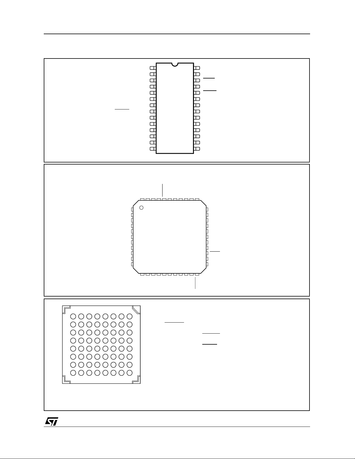
Figure 2. PIN CONNECTIONS
STA014-STA014B-STA014T
VDD_1
VSS_1
BIT_EN
SRC_INT/SCK_ADC
LRCKT
VSS_2
VDD_2
1
N.C.
2
LRCKT
3
OCLK
VSS_2
VDD_2
VSS_3
VDD_3
N.C.
PVDD
PVSS
4
5
6
7
8
9
10
GPSO_REQ
1
2
3
SCKT
SDO
IODATA[7]
4
5
6
7
SO28
8
9
10
11
12
13
D99AU1061
SRC_INT/SCK_ADC
IODATA[6]
SCL
SDI
SCKR
SDO
SCKT
OCLK
44 43 42 41 3940 38 37 36 35 34
BIT_EN
IODATA[5]
28
27
26
25
24
23
22
21
20
19
18
17
16
1514
IODATA[4]
TQFP44
XTI
IODATA[3]
171118 19 20 21 22
N.C.
VSS_4
IODATA[2]
IODATA[1]
12 13 14 15 16
FILT
XTO
OUT_CLK/DATA_REQ
LRCK_ADC
RESETSDA
SDI_ADC
TESTEN
VDD_4
VSS_4
XTI
XTO
FILT
PVSS
PVDD
VDD_3
VSS_3
SDI
GPIO/STROBE
SCKR
33
32
31
30
29
28
27
26
25
24
23
D99AU1062
VDD_4
TESTEN
IODATA[0]
GPSO_DATA
SCL
SDA
VSS_1
VDD_1
GPSO_SCKR
OUT_CLK/DATA_REC
LRCK_ADC
RESET
SDI_ADC
N.C.
12345678
A1 = SDI
A
B
C
D
E
F
G
H
B2 = SCKR
D4 = BIT_EN
D1 = SRC_INT
E2 = SDO
F2 = SCKT
H1 = LRCKT
H3 = OCLK
F3 = VSS_2
E4 = VDD_2
G4 = VSS_3
G5 = VDD_3
F5 = PVDD
G6 = PVSS
D00AU1149
G7 = FILT
G8 = XTO
F7 = XTI
E7 = VSS_4
C8 = VDD_4
D7 = TESTEN
A7 = SDI_ADC
B6 = RESET
A5 = LRCK_ADC
C5 = OUT_CLK/DATA_REQ
B5 = VDD_1
B4 = VSS_1
A4 = SDA
B3 = SCL
C2 = GPIO_STROBE
C3 = IODATA [4]
E3 = IODATA [5]
D2 = IODATA [6]
F1 = IODATA [7]
G3 = GPSO_REQ
F8 = IODATA [3]
F6 = IODATA [2]
E6 = IODATA [1]
C7 = IODATA [0]
C6 = GPSO_SCKR
A2 = GPSO_DATA
LFBGA64
3/45
Page 4
STA014-STA014B-STA014T
1. OVERVIEW
1.1 - MP3 decoder engine
The MP3 decoder engine is able to decode any
Layer III compliant bitstream: MPEG1, MPEG2
and MPEG2.5 streams are supported. Besides
audio data decoding the MP3 engine also performs ANCILLARY data extraction: these data
can be retrieved via I2C bus by the application
microcontroller in order to implement specific
functions.
Decoded audio data goes through a software volume control and a two-band equalizer blocks before feeding the output I2S interface. This results
in no need for an external audio processor.
MP3 bitstream is sent to the decoder using a simple serial input interface (see pins SDI, SCKR,
BIT_EN and DATA_REQ), supporting input rate
up to 20 Mbit/s. Received data are stored in a
256 bytes long input buffer which provides a
ABSOLUTE MAXIMUM RATINGS
feedback line (see DATA_REQ pin) to the bitstream source (tipically an MCU).
1.2 - ADPCM encoder/decoder engine
This device also embeds a multistandard ADPCM
encoder/decoder supporting different sample
rates (from 8 KHz up to 32 KHz) and different
sample sizes (from 8 bit to 32 bits). During encoding process two different interfaces can be
used to feed data: the serial input interface (same
interface used also to feed MP3 bitstream) or the
ADC input interface, which provides a seamless
connection with an external A/D converter. The
currently used interface is selected via I2C bus.
Also to retrieve encoded data two different interfaces are available: the I2C bus or the faster
GPSO output interface. GPSO interface is able to
output data with a bitrate up to 5 Mbit/s and its
control pins (GPSO_SCKR, GPSO_DATA and
GPSO_REQ) can be configured in order to easily
fit the target application.
Symbol Parameter Value Unit
V
DD
V
i
V
O
T
stg
T
oper
Power Supply -0.3 to 4 V
Voltage on Input pins -0.3 to VDD +0.3 V
Voltage on output pins -0.3 to VDD +0.3 V
Storage Temperature -40 to +150 °C
Operative ambient temp -20 to +85 °C
THERMAL DATA
Symbol Parameter Value Unit
R
th j-amb
Thermal resistance Junction to Ambient 85 °C/W
4/45
Page 5
STA014-STA014B-STA014T
PIN DESCRIPTION
SO28 TQFP44 LFBGA64 Pin Name Type Function PAD Description
1 29 B5 VDD_1 Supply Voltage
2 30 B4 VSS_1 Ground
3 31 A4 SDA I/O i
4 32 B3 SCL I I
5 34 A1 SDI I Receiver Serial Data CMOS Input Pad Buffer
6 36 B2 SCKR I Receiver Serial Clock CMOS Input Pad Buffer
7 38 D4 BIT_EN I Bit Enable CMOS Input Pad Buffer with
840 D1
SRC_INT/SCK_ADC I Interrupt Line/ADC Serial
9 42 E2 SDO O T ra n s m i t te r S e r ia l D a t a ( P C M D a t a ) CMOS 4mA Output Drive
10 44 F2 SCKT O Transmitter Serial Clock CMOS 4mA Output Drive
11 2 H1 LRCLKT O Transmitter Left/Right Clock CMOS 4mA Output Drive
12 3 H3 OCLK I/O Oversampling Clock for DAC CMOS Input Pad Buffer
13 5 F3 VSS_2 Ground
14 6 E4 VDD_2 Supply Voltage
15 7 G4 VSS_3 Ground
16 8 G5 VDD_3 Supply Voltage
17 10 F5 PVDD PLL Power
18 11 G6 PVSS PLL Ground
19 12 G7 FILT O PLL Filter Ext. Capacitor
20 13 G8 XTO O Crystal Output CMOS 4mA Output Drive
21 15 F7 XTI I Crystal Input (Clock Input) Specific Level Input Pad
22 19 E7 VSS_4 Ground
23 21 C8 VDD_4 Supply Voltage
24 22 D7
TESTEN I Test Enable CMOS Input Pad Buffer with
25 24 A7 SDI_ADC I ADC Data Input CMOS Input Pad Buffer
26 25 B6
RESET I System Reset CMOS Input Pad Buffer with
27 26 A5 LRCK_ADC I ADC Left/Right Clock CMOS Output Pad Buffer
28 27 C5 OUT_CLK/
DATA_REQ
20 C7 IODATA[0] I/O GPIO Data Line CMOS 4mA Schmitt Trigger
18 E6 IODATA[1] I/O GPIO Data Line
16 F6 IODATA[2] I/O GPIO Data Line
14 F8 IODATA[3] I/O GPIO Data Line
37 C3 IODATA[4] I/O GPIO Data Line
39 E3 IODATA[5] I/O GPIO Data Line
41 D2 IODATA[6] I/O GPIO Data Line
43 F1 IODATA[7] I/O GPIO Data Line
35 C2 GPIO_STROBE I/O GPIO Strobe Signal
4 G3 GPSO_REQ O GPSO Request Signal CMOS Output Pad Buffer
28 C6 GPSO_SCKR I GPSO Serial Clock CMOS Input Pad Buffer
33 A2 GPSO_DATA O GPSO Serial Data CMOS Output Pad Buffer
Note: In functional mode TESTEN must be connected to VDD.
2
C Serial Data +
Acknowledge
2
C Serial Clock CMOS Input Pad Buffer
CMOS Input Pad Buffer
CMOS 4mA Output Drive
pull up
CMOS Input Pad Buffer
Clock
CMOS 4mA Output Drive
Conn.
(see paragraph 2.1)
pull up
pull up
O Buffered Output Clock/
CMOS 4mA Output Drive
Data Request Signal
Bidir Pad Buffer
5/45
Page 6

STA014-STA014B-STA014T
1. ELECTRICAL CHARACTERISTICS:
DD
= 3.3V ±0.3V; T
V
amb
= 0 to 70°C; Rg = 50Ω unless otherwise
specified
DC OPERATING CONDITIONS
Symbol Parameter Value
V
T
GENERAL INTERFACE ELECTRICAL CHARACTERISTICS
Power Supply Voltage 2.4 to 3.6V
DD
Operating Junction Temperature -20 to 125°C
j
Symbol Parameter Test Condition Min. Typ. Max. Unit Note
I
IL
Low Level Input Current
Vi = 0V -10 10
A1
µ
Without pull-up device
I
IH
High Level Input Current
Vi = V
DD
-10 10
A1
µ
Without pull-up device
V
esd
Note 1:
The leakage currents are generally very small, < 1nA. The value given here is a maximum that can occur after an electrostatic stress
on the pin.
Note 2:
Human Body Model.
Electrostatic Protection Leakage < 1µA 2000 V 2
DC ELECTRICAL CHARACTERISTICS
Symbol Parameter Test Condition Min. Typ. Max. Unit Note
V
IL
V
IH
V
ol
V
oh
Low Level Input Voltage 0.2*V
High Level Input Voltage 0.8*V
Low Level Output Voltage I
= Xma 0.4V V 1, 2
ol
High Level Output Voltage 0.85*V
DD
DD
DD
V
V
V 1, 2
Note 1:
Takes into account 200mV voltage drop in both supply lines.
Note 2:
X is the source/sink current under worst case conditions and is reflected in the name of the I/O cell according to the drive capability.
Symbol Parameter Test Condition Min. Typ. Max. Unit Note
I
pu
Pull-up current Vi = 0V; pin numbers 7, 24
RpuEquivalent Pull-up
and 26
-25 -66 -125
50 k
A1
µ
Ω
Resistance
Note 1:
Min. condition: V
Max. condition: V
DD
= 2.7V, 125°C Min process
DD
= 3.6V, -20°C Max.
POWER DISSIPATION
Symbol Parameter Test Condition Min. Typ. Max. Unit Note
PD Power Dissipation
= 2.4V
@ V
DD
Sampling_freq ≤24 kHz 76 mW
Sampling_freq ≤32 kHz 79 mW
Sampling_freq ≤48 kHz 85 mW
6/45
Page 7

STA014-STA014B-STA014T
Figure 3.
Figure 4.
Test Circuit (refer to SO28 package)
OUT_CLK/DATA_REQ
V
DD
100nF
V
SS
V
DD
100nF
V
SS
V
DD
100nF
V
SS
V
DD
100nF
V
SS
PV
V
DD
DD
PV
V
SS
SS
28
1
2
14
13
16
15
23
22
17 18
100nF4.7µF 4.7µF
PV
DD
Test Load Circuit
V
DD
I
OL
SDA
3
SCL
4
SDO
9
SCKT
10
LRCKT
11
OCLK
12
SDI
5
SCKR
6
BIT_EN
7
SDI_ADC
25
SCR_INT
8
LRCK_ADC
27
XTI
21
XTO
20
19
26
RESET
PV
SS
24
TESTEN
D00AU1143
470pF
10K
1K
4.7nF
PV
SS
Test Load
Output I
OL
SDA 1mA 100pF 3.6V
Other Outputs 100µA100µA 100pF 1.5V
I
OH
C
V
L
REF
OUTPUT
C
I
L
OH
2. FUNCTIONAL DESC RI PTION
2.1 - Clock Signal
The STA014 input clock is derivated from an external source or from a industry standard crystal
oscillator, generating input frequencies of 10,
V
REF
D98AU967
Other frequencies may be supported upon request to STMicroelectronics. Each frequency is
supported by downloading a specific configuration file, provided by STM
XTI is an input Pad with specific levels.
14.31818 or 14.7456 MHz.
Symbol Parameter Test Condition Min. Typ. Max. Unit
V
IL
V
IH
Low Level Input Voltage VDD-1.8 V
High Level Input Voltage VDD-0.8 V
CMOS compatibility
The XTI pad low and high levels are CMOS compatible; XTI pad noise margin is better than typical
CMOS pads.
TTL compatibility
DD
The XTI pad low level is compatible with TTL while the high level is not compatible (for example if V
=
3V TTL min high level = 2.0V while XTI min high level = 2.2V)
7/45
Page 8
STA014-STA014B-STA014T
Figure 5.
PLL and Clocks Generation System
XTI
N
FRAC
Upda t e FR AC
Switching
Circuit
PFD CP
M
2.2 - PLL & Clock Generator System
When STA014 receives the input clock, as described in Section 2.1, and a valid layer III input
bitstream, the internal PLL locks, providing to the
DSP Core the master clock (DCLK), and to the
Audio Output Interface the nominal frequencies of
the incoming compressed bit stream. The STA014
PLL block dia gram is des cribed in F igure 5.
The audio sample rates are obtained dividing the
oversampling clock (OCLK) by software programmable factors. The operation is done by STA014 embedded softwar e and it is trans parent to the user .
The STA014 PLL can drive directly most of the commercial DACs families, providing an over sampling
clock, OCLK, obtained dividing the VCO frequ ency
with a software programmable dividers.
2.3 - STA014 Operational Modes
The device can be configured in 4 different operational modes. To select one specific mode a
dedicated CHIP_MODE registers is available. For
proper operation the following steps must be issued to switch between different modes:
- issue a software reset (SOFT_RESET register)
- select the desired mode (CHIP_MODE register)
- run the device (RUN register)
Hereby is a short description of each available
mode
ADPCM Encoder
This mode can be used to encode the incoming bitstream with 4 different compression algorithms. Moreover different sample frequencies and word size are supported. For a
detailed description of this features refer to the
related registers.
ADPCM Decoder
This mode can be used when an ADPCM
compressed bitstream must be decoded.
R
CC
VCO
Disable PLL
XTI2OCLK
X
S
XTI2DSPCLK
OCLK
DCLK
The input interface handling and control flow is
the same as in the MP3 Mode.
BYPASS mode
Using this mode it’s possible to use the embedded post-processing controls (volu me and
tone controls) to process an incoming uncompressed stereo audio stream. In this configuration ADC input is the only supported interface.
This could be useful , for instance, to process
audio data coming from an external tuner or
some other auxiliary source.
MP3 mode
In MP3 Mode (default mode) STA014 decodes
the incoming bitstream, acting as a master of
the data communication from the source to itself.
This control is done by a specific buffer management, controlled by STA014 embedded
software. The data coming from the serial interface are stored in the input buffer, a 256
bytes long FIFO.
The feedback line DATA_REQ actually is the
result of the h/w comparison between the writing address of the FIFO and the constant
value 252. This means that if the buffer is f illed
up with more than 252 bytes the DATA_REQ
line goes low, requesting MCU to stop transmission: the maximum time to stop transmitting is given by t he time required to t ransmit 4
bytes (this time, in turn, depends on the bitstream speed used to send MP3 data).
The input interface can receive data with a
speed up to 20Mbit/s. The speed at which the
FIFO is emptied is equ al to the MP3 nominal
bitrate. Provided the FIFO is filled up with 252
bytes the time required to empty it (in worst
condition, which is 320kbit/s mpeg stream) is
about 6ms. So if no more data is received in
this time the buffer will be emptied and this will
badly affect the output audio.
8/45
Page 9
STA014-STA014B-STA014T
In this mode the fractional part of the PLL is disabled and the audio clocks are generated at
nominal rates. Fig. 6 describes the default
DATA_REQ signal behaviour. Programming
STA014 it is possible to invert the polarity of the
DATA_REQ line (register REQ_POL).
Figure 6.
SOURCE STOPS TRANSMITTING DATA SOURCE STOPS TRANSMITTING DATA
DATA_REQ control line
DATA_REQ
SOURCE SEND DATA TO STA015
D00AU1144
2.4 - STA014 Decoding States
There are three different decoder states:
Init,
and
Decode.
Commands to change the de-
coding states are described in the STA014 I
Idle,
2
registers description.
Idle Mode
In this mode (entered after a S/W or H/W reset)
the decoder is waiting for the RUN command.
This mode should be used to initialize the con-
figuration registers of t he device. The DAC connected to STA014 can be initialized during this
mode (set MUTE to 1).
PLAY MUTE Clock State PCM Output
X 0 Not Running 0
X 1 Running 0
Init Mode
"PLAY" and "MUTE" changes are ignored in this
mode. The internal state of the decoder will be
updated only when the decoder changes from the
state "init" t o the state "decode". The "init" phase
ends when the first decoded samples are at the
output stage of the device.
Decode Mode
This mode is completely described by the following table:
C
PLAY MUTE Clock State
0 0 Not Running 0 No
0 1 Running 0 No
1 0 Running Decoded
1 1 Running 0 Yes
PCM
Output
Samples
Decoding
Yes
Figure 7.
MPEG Decoder Interfaces.
DATA_REQ
SDI
DATA
SOURCE
D98AU912
SCKR
BIT_EN
XTI FILT
XTO
PLL
MPEG
DECODER
SERIAL AUDIO INTERFACE
RX TX
µP
IIC
SCL SDA
IIC
SDO
SCKT
LRCKT
DAC
OCLK
9/45
Page 10

STA014-STA014B-STA014T
Figure 8.
Serial Input Interface Clocks
SDI
SCKR
SCKR
BIT_EN
D98AU968A
3. INTERFACE DESCRIPTION
3.1 - Serial I nput Interface
STA014 receives the input data (MSB first)
through the Serial Input Interface (Fig.7). It is a
serial communication interface connected to the
SDI (Serial Data Input) and SCKR (Receiver Serial Clock).
The interface can be configured to receive data
sampled on both rising and falling edge of the
SCKR clock. The BIT_EN pin, when set to low,
forces the bitstream input interface to ignore the
incoming data. For proper operation BIT_EN line
should be toggled only when SCKR is stable low
(for both SCLK_POL configuration)8The possible
configurations are described in Fig. 8.
3.2 - GPSO Output Interface
In order to retrieve ADPCM encoded data a General Purpose Serial Output interface is available
(in TQFP44 and LFBGA64 packages only). The
maximum frequency for GPSO_SCKR clock is
Figure 9.
PCM Output Fo rm a ts
LRCKT
SDO
SDO
16 SCLK Cycles
M
S
L
S
16 SCLK Cycles
M
SLS
L
M
S
S
DATA IGNORED
SCLK_POL=0
SCLK_POL=4
DATA IGNOREDDATA VALID
the DSP system clock frequency divided by 3
(i.e. 8.192 MHz @ 24.58MHz). The interface is
based on a simple and configur able 3- lines pr otocol, as described by figure 10.
3.3 - PCM Output Interface
The decoded audio data are output in serial PCM
format. The interface consists of the following signals:
SDO PCM Serial Data Output
SCKT PCM Serial Clock Output
LRCLK Left/Right Channel Selection Clock
The output samples precision is selectable from
16 to 24 bits/word, by setting t he output precision
with PCMCONF (16, 18, 20 and 24 bits mode)
register. Data can be output either with the most
significant bit first (MS) or least significant bit first
(LS), selected by writing into a flag of the
PCMCONF register.
Figure 8 gives a description of the several
STA014 PCM Output Formats. The sample rates
set decoded by STA014 is described in Table 1.
16 SCLK Cycles
L
M
S
S
L
M
S
S
16 SCLK Cycles
M
L
S
S
M
L
S
S
16 SCLK Cycles
PCM_ORD = 0
L
S
PCM_PREC is 16 bit mode
PCM_ORD = 1
M
PCM_PREC is 16 bit mode
S
Table 1:
10/45
LRCKT
SDO
SDO
SDO
SDO
32 SCLK Cycles
M
L
S
S
0
LSM
0
S
M
S
32 SCLK Cycles
M
S
L
0
SMS
M
0
00
S
L
MSBMSB
S
L
00
S
M
S
L
S
M
S
32 SCLK Cycles
L
M
S
S
L
M
0
S
S
M
L
0
S
S
MSL
L
MSB MSB
S
32 SCLK Cycles
32 SCLK Cycles
L
S
M
S
S
00
L
S
PCM_FORMAT = 1
PCM_DIFF = 1
PCM_FORMAT = 0
L
PCM_DIFF = 0
S
PCM_FORMAT = 0
PCM_DIFF = 1
PCM_FORMAT = 1
LSM
PCM_DIFF = 1
M
S
L
0
S
M
0
00
S
S
MPEG Sampling Rates (KHz)
MPEG 1 MPEG 2 MPEG 2.5
48 24 12
44.1 22.05 11.025
32 16 8
Page 11

Figure 10.
GPSO_SCKR
GPSO_REQ
GPSO_SCKR
GPSO_DATA
GPSO_REQ
STA014-STA014B-STA014T
MCU
GPSO_DATA
To enable the GPSO interface bit GEN of
GPSO_ENABLE register must be set. Using the
GPSO_CONF register the protocol can be configured in order to provide outcoming data on ris-
ADPCM encoding mode to provide an interrupt;
other pins are reserved for future use. The related configuration register is GPIO_CONF. See
the following summary for related pin usage:
D00AU1145
ing/falling edge of GPSO_SCKR input clock; the
GPSO_REQ request signal polarity (usually connected to an MCU interrupt line) can be configured as well.
3.4 ADC Inteface
Name Description Dir
I/ODATA [0]
GPIO data line I/O
....................
I/ODATA [7]
GPIO_STROBE GPIO strobe line I/O
Beside the serial input interface based on SDI
and SCKR lines a 3 wire flexible and user conf ig-
4 ADPCM ENCODING: Overview
urable input interface is also available, suitable to
interface with most A/D converters. To configure
this interface 4 specific I
(ADC_ENABLE, ADC_CONF, ADC_WLEN and
ADC_WPOS). Refer to registers description for
more details.
3.5 General Purpose I/O Interface
A new general purpose I/O interface has been
added to this device (TQFP44 and LFBGA64
only). Actually only the strobe line is used in
INPUT (data to encode) Output (encoded data)
ADC I/F (SDI_ADC + LRCK_ADC + SCK_ADC) GPSO I/F (GPSO_REQ + GPSO_DATA +
ADC I/F (SDI_ADC + LRCK_ADC + SCK_ADC) I
SERIAL I/F (SCKR + SDI + DATA_REQ) GPSO I/F (GPSO_REQ + GPSO_DATA +
SERIAL I/F (SCKR + SDI + DATA_REQ) (*) I
(*) STA013 Compatible mode
2
C registers are available
GPSO_SCKR)
2
GPSO_SCKR)
2
According to the previously described interfaces
there are 4 ways to manage ADPCM data stream
while encoding. Input int erface can be either the
serial receiver block (SDI + SCKR + DATA_REQ
lines) or the ADC specific interface.
Output interfaces can be either t he I
or without interrupt line) or the GPSO high-speed
serial interface (GPSO_REQ + GPSO_ DATA +
GPSO_SCKR lines). This result in the following 4
methods to handle encoding flow:
C + Interrupt (SCL + SDA + DATA_REQ) SO28/TQFP44
C (polling) (SCL + SDA) SO28/TQFP44
Figure. 11
....
I/O
2
C bus (with
Available on
package
TQFP44
LFBGA64
LFBGA64
TQFP44
LFBGA64
LFBGA64
LRCK_ADC
SDI_ADC
SCK_ADC
SDI
SCKR
DATA_REQ
ADC I/F
SERIAL
RECEIVER
ENCOD
ENGINE
GPSOMUX
I2C
D99AU1064
GPSO_REQ
GPSO_DATA
GPSO_SCKR
SDA
SCL
DATA_REQ
11/45
Page 12
STA014-STA014B-STA014T
The following 4 figures (fig. 12, 13, 14, 15) show
the available connection diagrams as far as
ADPCM encoding function. As shown in the figures some configuration is not available in SO28
package.
Figure 12.
Input from BITSTREAM, Output from
I2C
SDI
SCKR
DATA_REQ
MCU DAC
BIT_EN
2
C
I
SO28
TQFP44
LFBGA64
LRCKT
SCKT
SDO
OCLK
D99AU1121A
STA013 compatible mode
Figure 14.
Input from BITSTREAM, Output from
GPSO
GPSO_DATA
GPSO_SCKR
GPSO_REQ
SDI
SCKR
DATA_REQ
MCU DAC
BIT_EN
2
C
I
TQFP44
LFBGA64
LRCKT
SCKT
SDO
OCLK
D99AU1122A
Figure 13.
DATA_REQ
MCU
ADC
SLAVE
MCU
ADC
MASTER
Figure 15.
GPSO_SCKR
MCU
ADC
MASTER
Input from ADC, Output from I2C +
IRQ
2
I
C
LRCKT
SCKT
SDO
SDI_ADC
2
C
I
DATA_REQ
LRCK_ADC
SCK_ADC
SDI_ADC
SO28
TQFP44
LFBGA64
SO28
TQFP44
LFBGA64
OCLK
LRCKT
SCKT
SDO
OCLK
Input from ADC, Output from GPSO
GPSO_DATA
GPSO_REQ
LRCK_ADC
SCK_ADC
SDI_ADC
TQFP44
LFBGA64
LRCKT
SCKT
SDO
OCLK
DAC
DAC
D99AU1123A
DAC
D99AU1124A
5 - I2C BUS SPECIFICATION
2
The STA014 supports the I
C protocol. This protocol defines any device that sends data on to the
bus as a transmitter and any device that reads
the data as a receiver. The device that controls
the data transfer is known as the master and the
others as the slave. The master always starts the
transfer and provides the serial clock for synchronisation. The STA014 is always a slave device in
all its communications.
12/45
5. 1 - COMMUNICATION PROTOCOL
5.1.0 - Data transition or change
Data changes on the SDA line must only occur
when the SCL clock is low. SDA transition while
the clock is high are used to identify START or
STOP condition.
5.1.1 - Start condition
START is identified by a high to low transition of
the data bus SDA signal while the clock signal
SCL is stable in the high state.
A START condition must precede any command
for data trans fer.
Page 13
STA014-STA014B-STA014T
5.1.2 - Stop condition
STOP is identified by low to high transition of the
data bus SDA signal while the clock signal SCL is
stable in the high state. A STOP condition terminates communications between STA014 and the
bus master.
5.1.3 - Acknowledge bit
An acknowledge bit is used to indicate a successful data transfer. The bus transmitter, either master or slave, releases the SDA bus after sending
8 bit of data.
During the 9th clock pulse the receiver pulls the
SDA bus low to acknowledge the receipt of 8 bits
of data.
5.1.4 - Data input
During the data input the STA014 samples the
SDA signal on the rising edge of the clock SCL.
For correct device operation the SDA signal has
to be stable during the rising edge of the clock
and the data can change only when the SCL line
is low.
5.2 - DEVICE ADDRESSIN
G
To start communication between the master and
the STA014, the master must i nitiate with a start
condition. Following this, the master sends onto
the SDA line 8 bits (MSB first) corresponding to
the device select address and read or write
mode.
Figure 16.
Write Mode Sequence
The 7 most significant bits are the device address
identifier, corresponding to the I
2
C bus definition.
For the STA014 these are fixed as 1000011.
The 8th bit (LSB) is the read or write operation
RW, this bit is set to 1 in read mode and 0 for
write mode. After a START condition the STA014
identifies on the bus the device addr ess and, if a
match is found, it acknowledges the identification
on SDA bus during the 9th bit t ime. The following
byte after t he device identification byte is t he internal space address.
5.3 - WRITE OPERATION
(see fig. 16)
Following a START condition the master sends a
device select code with the RW bit set to 0.
The STA014 acknowledges this and waits for the
byte of internal address.
After receiving the internal bytes address the
STA014 again responds with an acknowledge.
5.3.1 - Byte write
In the byte write mode the master sends one data
byte, this is acknowledged by STA014. The master then terminates the transfer by generating a
STOP condition.
5.3.2 - Multibyte write
The multibyte write mode can start from any internal address. The transfer is terminated by the
master generating a STOP condition.
Figure 17.
CURRENT
ADDRESS
READ
START
RANDOM
ADDRESS
READ
START
SEQUENTIAL
CURRENT
READ
START
SEQUENTIAL
RANDOM
READ
START
BYTE
WRITE
MULTIBYTE
WRITE
DEV-ADDR
START
DEV-ADDR
START
Read Mode Sequence
ACK
DEV-ADDR
RW
ACK
DEV-ADDR
RW
RW=
ACK
HIGH
DEV-ADDR
ACK
DEV-ADDR
RW
DATA
SUB-ADDR
DATA
SUB-ADDR
ACK
RW
ACK
RW
NO ACK
ACK
START RW
ACK
ACK
START RW
SUB-ADDR
SUB-ADDR
STOP
DATA
DEV-ADDR
DEV-ADDR
ACK
ACK
ACK
ACK
ACK
DATA IN
DATA IN
DATA
DATA
DATA
ACK
ACK
STOP
NO ACK
NO ACK
ACK
D98AU825B
STOP
STOP
DATA
DATA IN
ACK
ACK NO ACK
D98AU826A
STOP
DATA
STOP
13/45
Page 14
STA014-STA014B-STA014T
5.4 - READ OPERATION
(see Fig. 17)
5.4.1 - Current byte address read
The STA014 has an internal byte address
counter. Each time a byte is written or read, this
counter is incremented.
For the current byte address read mode, f ollowing a START condition the master sends the device address with the RW bit set to 1.
The STA014 acknowledges this and outputs the
byte addressed by the internal byte address
counter. The master does not acknowledge the
received byte, but terminates the t ransfer with a
STOP condition.
5.4.2 - Sequential address read
This mode can be initiated with either a current
address read or a random address read. However in this case the master does acknowledge
the data byte output and the STA014 continues to
output the next byte in sequence.
To terminate the streams of bytes the master
does not acknowledge the last received byte, but
2
I
C REGISTERS
terminates the transfer with a STOP condition.
The output data stream is from consecutive byte
addresses, with the internal byte address counter
automatically incremented after one byte output.
2
C REGISTERS
6 - I
The following table gives a description of the
MPEG Source Decoder (STA014) register list.
The first column (HEX_COD) is the hexadecimal
code for the sub-address.
The second column (DEC_COD) is the decimal
code.
The third column (DESCRIPTION) is the description of the information contained in the register.
The fourth column (RESET) inidicate the reset
value if any. When no reset value is specifyed,
the default is "undefined".
The fifth column (R/W) is the flag to distinguish
register "read only" and "read and write", and the
useful size of the register itself.
Each register is 8 bit wide. The master shall operate reading or writing on 8 bits only.
HEX_COD DEC_COD DESCRIPTION RESET R/W
$00 0 VERSION R (8)
$01 1 IDENT 0xAC R (8)
$05 5 PLLCTL [7:0] 0xA1 R/W (8)
$06 6 PLLCTL [20:16] (MF[4:0]=M) 0x0C R/W (8)
$07 7 PLLCTL [15:12] (IDF[3:0]=N) 0x00 R/W (8)
$0C 12 REQ_POL 0x01 R/W (8)
$0D 13 SCLK_POL 0x04 R/W (8)
$0F 15 ERROR_CODE 0x00 R (8)
$10 16 SOFT_RESET 0x00 W (8)
$13 19 PLAY 0x01 R/W(8)
$14 20 MUTE 0x00 R/W(8)
$16 22 CMD_INTERRUPT 0x00 R/W(8)
$18 24 DATA_REQ_ENABLE 0x00 R/W(8)
$40 - $51 64 - 81 ADPCM_DATA_1 to ADPCM_DATA_18 0x00 R/W (8)
$40 64 SYNCSTATUS 0x00 R (8)
$41 65 ANCCOUNT_L 0x00 R (8)
$42 66 ANCCOUNT_H 0x00 R (8)
$43 67 HEAD_H[23:16] 0x00 R(8)
$44 68 HEAD_M[15:8] 0x00 R(8)
$45 69 HEAD_L[7:0] 0x00 R(8)
$46 70 DLA 0x00 R/W (8)
$47 71 DLB 0xFF R/W (8)
$48 72 DRA 0x00 R/W (8)
$49 73 DRB 0xFF R/W (8)
$4D 77 CHIP_MODE 0x00 R/W (2)
14/45
Page 15

STA014-STA014B-STA014T
2
I
C REGISTERS
HEX_COD DEC_COD DESCRIPTION RESET R/W
$4E 78 CRCR 0x00 R/W (1)
$50 80 MFSDF_441 0x00 R/W (8)
$51 81 PLLFRAC_441_L 0x00 R/W (8)
$52 82 ADPCM_DATA_READY 0x00 R/W (1)
$52 82 PLLFRAC_441_H 0x00 R/W (8)
$53 83 ADPCM_SAMPLE_FREQ 0x00 R/W (4)
$54 84 PCM DIVIDER 0x03 R/W (8)
$55 85 PCMCONF 0x21 R/W (8)
$56 86 PCMCROSS 0x00 R/W (8)
$61 97 MFSDF (X) 0x07 R/W (8)
$63 99 DAC_CLK_MODE 0x00 R/W (8)
$64 100 PLLFRAC_L 0x46 R/W (8)
$65 101 PLLFRAC_H 0x5B R/W (8)
$67 103 FRAME_CNT_L 0x00 R (8)
$68 104 FRAME_CNT_M 0x00 R (8)
$69 105 FRAME_CNT_H 0x00 R (8)
$6A 106 AVERAGE_BITRATE 0x00 R (8)
$71 113 SOFTVERSION R (8)
$72 114 RUN 0x00 R/W (8)
$77 119 TREBLE_FREQUENCY_LOW 0x00 R/W (8)
$78 120 TREBLE_FREQUENCY_HIGH 0x00 R/W (8)
$79 121 BASS_FREQUENCY_LOW 0x00 R/W (8)
$7A 122 BASS_FREQUENCY_HIGH 0x00 R/W (8)
$7B 123 TREBLE_ENHANCE 0x00 R/W (8)
$7C 124 BASS_ENHANCE 0x00 R/W (8)
$7D 125 TONE_ATTEN 0x00 R/W (8)
$7E - B5 126 - 181 ANC_DATA_1 to ANC_DATA_56 0x00 R (8)
$B6 182 ISR 0x00 R/W (1)
$B8 184 ADPCM_CONFIG 0x00 R/W (2)
$B9 185 GPSO_ENABLE 0x00 R/W (1)
$BA 186 GPSO_CONF 0x00 R/W (2)
$BB 187 ADC_ENABLE 0x00 R/W (1)
$BC 188 ADC_CONF 0x00 R/W (5)
$BD 189 ADPCM_FRAME_SIZE 0x00 R/W (8)
$BE 190 ADPCM_INT_CFG 0x00 R/W (8)
$BF 191 GPIO_CONF 0x00 R/W (2)
$C0 192 ADC_ WLEN 0x0F R/W (5)
$C1 193 ADC_ WPOS 0x00 R/W (5)
$C2 194 ADPCM_SKIP_FRAME 0x00 R/W (8)
$C3 195 WOW_ENABLE 0x00 R/W (8)
$C4 196 WOW_SPK_MODE 0x00 R/W (8)
$C5 197 WOW_TRUEBASS 0x00 R/W (8)
$C6 198 WOW_ FOCUS 0x00 R/W (8)
Note:
1) The HEX_COD is the hexadecimal adress that the microcont rol l er has to gener ate to access the informat io n.
2) RESERVED: register used for producti on tes t only, or for future use.
(continued)
15/45
Page 16

STA014-STA014B-STA014T
6.1 - STA014 REGISTERS DESCRIPTION
2
The STA014 device includes 256 I
C registers. In
this document, only the user-oriented registers
are described. The undocumented registers are
reserved. These registers must never be accessed (in Read or in Write mode). The ReadOnly registers must never be written.
The following table describes the meaning of the
abbreviations used in the I
2
C registers descrip-
tion:
Symbol Comment
NA Not Applicable
UND Undefined
NC No Charge
RO Read Only
WO Write Only
R/W Read and Write
R/WS Read, Write in specific mode
VERSION
Address: 0x00 (00)
Type: RO
MSB LSB
b7 b6 b5 b4 b3 b2 b1 b0
V8 V7 V6 V5 V4 V3 V2 V1
The VERSION register is read-only and it is used
to identify the IC on the application board.
PLLCTL
Address: 0x05 (05)
Type: R/W
Software Reset: 0xA1
Hardware Reset: 0xA1
MSB LSB
b7 b6 b5 b4 b3 b2 b1 b0
XTO_
XTODISOCLKENSYS2O
BUF
CLK
PPLDISXTI2DS
PCLK
XTI2O
CLK
UPD_F
RAC
UPD_FRAC: when is set to 1, update FRAC in
the switching circuit. It is set to 1 after autoboot.
XTI2OCLK: when is set to 1, use the XTI as input
of the divider X instead of VCO output. It is set to
0 on HW reset.
XTI2DSPCLK: when is to 1, set use the XTI as input of the divider S instead of VCO output. It is
set to 0 on HW reset.
PLLDIS: when set to 1, the VCO output is disabled. It is set to 0 on HW reset.
SYS2OCLK: when is set to 1, the OCLK frequency is equal to the system frequency. It is
useful for testing. It is set to 0 on HW reset.
OCLKEN: when is set to 1, the OCLK pad is enable as output pad. It is set to 1 on HW reset.
XTODIS: when is set to 1, the XTO pad is disable. It is set to 0 on HW reset.
XTO_BUF: when this bit is set, the pin nr. 28
(OUT_CLOCK/DATA_REQ) is enabled. It is set
to 0 after autoboot.
IDENT
Address: 0x01 (01)
Type: RO
Software Reset: 0xAC
Hardware Reset: 0xAC
MSB LSB
b7 b6 b5 b4 b3 b2 b1 b0
10101100
IDENT is a read-only register and is used to id entify the IC on an application board. IDENT always
has the value "0xAC"
16/45
PLLCTL (M)
Address: 0x06 (06)
Type: R/W
Software Reset: 0x0C
Hardware Reset: 0x0C
PLLCTL (N)
Address: 0x07 (07)
Type: R/W
Software Reset: 0x00
Hardware Reset: 0x00
The M and N registers are used to conf igure the
STA014 PLL by DSP embedded software.
M and N registers are R/W type but they are
completely controlled, on STA014, by DSP software.
Page 17

STA014-STA014B-STA014T
REQ_POL
Address: 0x0C (12)
Type: R/W
Software Reset: 0x01
Hardware Reset: 0x00
The REQ_POL registers is used to program the
polarity of the DATA_REQ line.
MSB LSB
b7 b6 b5 b4 b3 b2 b1 b0
00000001
Default polarity (the source sends data when the
DATA_REQ line is high)
MSB LSB
b7 b6 b5 b4 b3 b2 b1 b0
00000101
Inverted polarity (the source sends data when the
DATA_REQ line is low)
SCLK_POL
Address: 0x0D (13)
Type: R/W
Software Reset: 0x04
Hardware Reset: 0x04
MSB LSB
b7 b6 b5 b4 b3 b2 b1 b0
XXXXX000(1)
100(2)
X = don’t care
SCLK_POL is used to select the working polarity
of the Input Serial Clock (SCKR).
(1) If SCLK_POL is set to 0x00, the data (SDI)
are sent with the falling edge of SCKR
and sampled on the rising edge.
(2) If SCLK_POL is set to 0x04, the data (SDI)
are sent with the rising edge of SCKR and
sampled on the falling edge.
ERROR_CODE
Address: 0x0F (15)
Type: RO
Software Reset: 0x00
Hardware Reset: 0x00
MSB LSB
b7 b6 b5 b4 b3 b2 b1 b0
X X EC5 EC4 EC3 EC2 EC1 EC0
X = don’t care
ERROR_CODE register contains the last error
occourred if any. The codes can be as follows:
Code Description
0x00 No error since the last SW or HW Reset
0x01 CRC Failure
0x02 DATA not available
0x04 Ancillary data not read
0x10 Audio synch word not found
0x2X MPEG Header error
0x3X MPEG Decoding errors
SOFT_RESET
Address: 0x10 (16)
Type: WO
Software Reset: 0x00
Hardware Reset: 0x00
MSB LSB
b7 b6 b5 b4 b3 b2 b1 b0
XXXXXXX0
1
X = don’t care; 0 = normal operation; 1 = reset
When this register is written, a soft reset occours.
The STA014 core command register and the interrupt register are cleared. The decoder goes in
to idle mode.
PLAY
Address: 0x13 (19)
Type: R/W
Software Reset: 0x01
Hardware Reset: 0x01
MSB LSB
b7 b6 b5 b4 b3 b2 b1 b0
XXXXXXX0
1
X = don’t care; 0 = normal operation; 1 = play
The PLAY command is handled according to the
state of the decoder, as described in section 2.5.
PLAY only becomes active when the decoder is
in DECODE mode.
17/45
Page 18

STA014-STA014B-STA014T
MUTE
Address: 0x14 (20)
Type: R/W
Software Reset: 0x00
Hardware Reset: 0x00
MSB LSB
b7 b6 b5 b4 b3 b2 b1 b0
XXXXXXX0
1
X = don’t care; 0 = normal operation; 1 = mute
The MUTE command is handled according to the
state of the decoder, as described in section 2.5.
MUTE sets the clock running.
DATA_REQ_ENABLE
Address: 0x18 (24)
Type: R/W
Software Reset: 0x00
Hardware Reset: 0x00
CMD_INTERRUPT
Address: 0x16 (22)
Type: R/W
Software Reset: 0x00
Hardware Reset: 0x00
MSB LSB
b7 b6 b5 b4 b3 b2 b1 b0
XXXXXXX0
1
X = don’t care;
0 = normal operation;
1 = write into I
2
C/Ancillary Data
The INTERRUPT is used to give STA014 the
command to write into the I2C/Ancillary Data
Buffer (Registers: 0x7E ... 0xB5). Every time the
Master has to extract the new buffer content it
writes into this register, setting it to a non-zero
value.
MSB LSB
b7 b6 b5 b4 b3 b2 b1 b0 Description
X X X X X 0 X X buffered output clock
X X X X X 1 X X request signal
The DATA_REQ_ENABLE register is used to
configure Pin n. 28 working as buffered output
clock or data request signal, used for multimedia
mode.
The buffered Output Clock has the same fre-
quency than the input clock (XTI)
SYNCSTATUS
Address: 0x40 (64)
Type: RO
Software Reset: 0x00
Hardware Reset: 0x00
MSB LSB
b7 b6 b5 b4 b3 b2 b1 b0 Description
XXXXXXSS1SS0
0 0 Research of sync word
0 1 Wait for Confirmation
1 0 Synchronised
18/45
Page 19

STA014-STA014B-STA014T
ADPCM_DATA BUFFER
Address: 0x40 - 0x51 (64 - 81)
Type: R/W
Software Reset: 0x00
Hardware Reset: 0x00
MSB LSB
b7 b6 b5 b4 b3 b2 b1 b0
ENCODED DATA N to N+18
ANCCOUNT_L
Address: 0x41 (65)
Type: RO
Software Reset: 0x00
Hardware Reset: 0x00
MSB LSB
b7 b6 b5 b4 b3 b2 b1 b0
AC7 AC6 AC5 AC4 AC3 AC2 AC1 AC0
ANCCOUNT_H
Address: 0x42 (66)
Type: RO
Software Reset: 0x00
Hardware Reset: 0x00
ANCCOUNT_H
MSB LSB
b7 b6 b5 b4 b3 b2 b1 b0
AC15 AC14 AC13 AC 12 AC11 AC10 AC9 AC8
ANCCOUNT registers are logically concatenated
and indicate the number of Ancillary Data bits
available at every correctly decoded MPEG
frame.
HEAD_H[23:16]
MSB LSB
b7 b6 b5 b4 b3 b2 b1 b0
X X X H20 H19 H18 H17 H16
x = don’t care
HEAD_L[7:0]
MSB LSB
b7 b6 b5 b4 b3 b2 b1 b0
H7 H6 H5 H4 H3 H2 H1 H0
Address: 0x43, 0x44, 0x45 (67, 68, 69)
Type: RO
Software Reset: 0x00
Hardware Reset: 0x00
Head[1:0] emphasis
Head[2] original/copy
Head[3] copyrightHead
[5:4] mode extension
Head[7:6] mode
Head[8] private bit
Head[9] padding bit
Head[11:10] sampling frequency index
Head[15:12] bitrate index
Head[16] protection bit
Head[18:17] layer
Head[19] ID
Head[20] ID_ex
The HEAD registers can be viewed as logically
concatenated to store the MPEG Layer III Header
content. The set of three registers is updated
every time the synchronisation to the new MPEG
frame is achieved
The meaning of the flags are shown in the following tables:
MPEG IDs
IDex ID
0 0 MPEG 2.5
0 1 reserved
1 0 MPEG 2
1 1 MPEG 1
Layer
in Layer III these two flags must be set always to
"01".
HEAD_M[15:8]
MSB LSB
b7 b6 b5 b4 b3 b2 b1 b0
H15 H14 H13 H12 H1‘1 H10 H9 H8
Protection_bit
It equals "1" if no redundancy has been added
and "0" if redundancy has been added.
19/45
Page 20

STA014-STA014B-STA014T
Bitrate_index
indicates the bitrate ( Kbit/sec) depending on the
MPEG ID.
bitrate index ID = 1 ID = 0
’0000’ free free
’0001’ 32 8
’0010’ 40 16
’0011’ 48 24
’0100’ 56 32
’0101’ 64 40
’0110’ 80 48
’0111’ 96 56
’1000’ 112 64
’1001’ 128 80
’1010’ 160 96
’1011’ 192 112
’1100’ 224 128
’1101’ 256 144
’1110’ 320 160
’1111’ forbidden forbidden
Sampling Frequency
indicates the sampling frequency of the encoded
audio signal (KHz) depending on the MPEG ID
Sampling
Frequency
’00’ 44.1 22.05 11.03
’01’ 48 24 12
’10’ 32 16 8
’11’ reserved reserved reserved
MPEG1 MPEG2 MPEG2.5
Private bit
Bit for private use. This bit will not be used in the
future b y IS O/IEC.
Mode
Indicates the mode according to the following table. The joint stereo mode is intensity_stereo
and/or ms_stereo.
mode mode specified
’00’ stereo
’01’ joint stereo (intensity_stereo and/or ms_stereo)
’10’ dual_channel
’11’ single_channel (mono)
Mode extension
These bits are used in joint stereo mode. They indicates which type of joint stereo coding method
is applied. The frequency ranges, over which the
intensity_stereo and ms_stereo modes are applied, are implicit in the algorithm.
Copyright
If this bit is equal to ’0’, there is no copyright on
the bitstream, ’1’ means copyright protected.
Original/Copy
This bit equals ’0’ if the bitstream is a copy, ’1’ if it
is original.
Emphasis
Indicates the type of de-emphasis that shall be
used.
Padding bit
if this bit equals ’1’, the frame contains an addi-
tional slot to adjust the mean bitrate to the sampling frequency, otherwise this bit is set to ’0’.
emphasis emphasis specified
’00’ none
’01’ 50/15 microseconds
’10’ reserved
’11’ CCITT J,17
DLA
Address: 0x46 (70)
Type: R/W
Software Reset: 0x00
Hardware Reset: 0x00
MSB LSB
b7 b6 b5 b4 b3 b2 b1 b0 Description
DLA7 DLA6 DLA5 DLA4 DLA3 DLA2 DLA1 DLA0 OUTPUT ATTENUATION
00000000 NO ATTENUATION
00000001 -1dB
00000010 -2dB
:::::::: :
01100000 -96dB
20/45
Page 21

STA014-STA014B-STA014T
DLA register is used to attenuate the level of
audio output at the Left Channel using the butterfly shown in Fig. 18. When the register is set to
Figure 18.
Volume Control and Output Setup
DLA
X
DLB
X
DRB
X
DRA
DSP Right Channel
X
255 (0xFF), the maximum attenuation is
achieved.
A decimal unit correspond to an attenuation step
of 1 dB.
Output Left ChannelDSP Left Channel
+
Output Right Channel
+
D97AU667
DLB
Address: 0x47 (71)
Type: R/W
Software Reset: 0xFF
Hardware Reset: 0xFF
MSB LSB
b7 b6 b5 b4 b3 b2 b1 b0 Description
DLB7 DLB6 DLB5 DLB4 DLB3 DLB2 DLB1 DLB0 OUTPUT ATTENUATION
00000000 NO ATTENUATION
00000001 -1dB
00000010 -2dB
:::::::: :
01100000 -96dB
DLB register is used to re-direct the Left Channel
on the Right, or to mix both the Channels.
Default value is 0x00, corresponding at the maximum attenuation in the re-direction channel.
DRA
Address: 0x48 (72)
Type: R/W
Software Reset: 0X00
Hardware Reset: 0X00
MSB LSB
b7 b6 b5 b4 b3 b2 b1 b0 Description
DRA7 DRA6 DRA5 DRA4 DRA3 DRA2 DRA1 DRA0 OUTPUT ATTENUATION
00000000 NO ATTENUATION
00000001 -1dB
00000010 -2dB
:::::::: :
01100000 -96dB
DRA register is used to attenuate the level of
audio output at the Right Channel using the butterfly shown in Fig. 11. When the register is set to
255 (0xFF), the maximum attenuation is
achieved.
A decimal unit correspond to an attenuation step
of 1 dB.
21/45
Page 22

STA014-STA014B-STA014T
DRB
Address: 0x49 (73)
Type: R/W
Software Reset: 0xFF
Hardware Reset: 0xFF
MSB LSB
b7 b6 b5 b4 b3 b2 b1 b0 Description
DRB7 DRB6 DRB5 DRB4 DRB3 DRB2 DRB1 DRB0 OUTPUT ATTENUATION
00000000 NO ATTENUATION
00000001 -1dB
00000010 -2dB
:::::::: :
01100000 -96dB
DRB register is used to re-direct the Right Channel on the Left, or to mix both the Channels.
CHIP_MODE
Address: 0x4D (77)
Type: R/W
Hardware Reset: 0x00
Using this register it’s possible to select which op-
eration will be performed by the DSP.
Possible values are:
0x00 - MP3 decoding
0x01 - Reserved
0x02 - ADPCM Encoder
0x03 - ADPCM Decoder
0x04 - BYPASS mode
The DSP will check for the value of this register
right after the RUN command has been issued
(refer to RUN register). After that no more checks
will be performed: therefore a SOFT_RESET
must be generated in order to change the dev ice
mode.
CRCR
Address: 0x4E (78)
Type: R/W
Software Reset: 0x00
Hardware Reset: 0x00
MSB LSB
b7 b6 b5 b4 b3 b2 b1 b0
XXXXXXXCRCEN
Default value is 0x00, corresponding at the maximum attenuation in the re-direction channel.
against the hardware one. If a discrepance occurs, the current frame is skipped and the decoder is muted. The ERROR_CODE register is
affected with the value 0x01.
If CRC_EN bit is set, the result of the CRC check
is ignored, but the ERROR_CODE register is
nevertheless affected wit h the value 0x01 if a discrepance has occurred.
MFSDF_441
Address: 0x50 (80)
Type: R/W
Software Reset: 0x00
Hardware Reset: 0x00
MSB LSB
b7 b6 b5 b4 b3 b2 b1 b0
X X X M4 M3 M2 M1 M0
This register contains the value for the PLL X
driver for the 44.1KHz reference frequency.
The VCO output frequency, when decoding
44.1KHz bitstream, is divided by (MFSDF_441 +1)
PLLFRAC_441_L
Address: 0x51 (81)
Type: R/W
Software Reset: 0x00
Hardware Reset: 0x00
The CRC register is used to enable/disable the
CRC check. If CRC_EN bit is cleared, the CRC
value encoded in the bitstream is checked
22/45
MSB LSB
b7 b6 b5 b4 b3 b2 b1 b0
PF7 PF6 PF5 PF4 PF3 PF2 PF1 PF0
Page 23

STA014-STA014B-STA014T
ADPCM_DATA_READY
Address: 0x52 (82)
Type: R/W
Software Reset: 0x00
Hardware Reset: 0x00
MSB LSB
b7 b6 b5 b4 b3 b2 b1 b0
XXXXXXXADR
ADR: Adpcm Data Ready
This bit signal ADPCM encoded data are ready to
be retrieved.
PLLFRAC_441_H
Address: 0x52 (82)
Type: R/W
Software Reset: 0x00
Hardware Reset: 0x00
MSB LSB
b7 b6 b5 b4 b3 b2 b1 b0
PF15 PF14 PF13 PF12 PF11 PF10 PF9 PF8
ADPCM_SAMPLE_FREQ
Address: 0x53 (83)
Type: R/W
Software Reset: 0x00
Hardware Reset: 0x00
MSB LSB
b7 b6 b5 b4 b3 b2 b1 b0
X X X ADPCM_SF
ADPCM_SF: Adpcm Sample Frequency
0x02 8KHz
0x0A 16KHz
0x0E 32KHz
PCMDIVIDER
Address: 0x54 (84)
Type: RW
Software Reset: 0x01
Hardware Reset: 0x01
76543210
PD7 PD6 PD5 PD4 PD3 PD2 PD1 PD0
The registers are considered logically concatenated and contain the fractional values for the
PLL, for 44.1KHz reference frequency.
(see also PLLFRAC_L and PLLFRAC_H registers)
PCMDIVIDER is used to set the frequency ratio
between the OCLK (Oversampling Clock for
DACs), and the SCKT (Serial Audio Transmitter
Clock).
The relation is the following:
SCKT_freq =
OCLK_freq
2 (1 + PCM_D IV
)
23/45
Page 24

STA014-STA014B-STA014T
The Oversampling Factor (O_FAC) is related to OCLK and SCKT by the following expression:
1) OCLK_freq = O_FAC * LRCKT_ Freq
(DAC relation)
2) OCLK_ Freq = 2 * (1+PCM_DIV) * 32*
LRCKT_Freq (when 16 bit PCM mode is used)
3) OCLK_ Freq = 2 * (1+PCM_DIV) * 64*
LRCKT_Freq (when 32 bit PCM mode is used)
4) PCM_DIV = (O_FAC/64) - 1 in 16 bit mode
5) PCM_DIV = (O_FAC/128) - 1 in 32 bit mode
Example for setting:
MSB LSB
b7 b6 b5 b4 b3 b2 b1 b0 Description
PD7 PD6 PD5 PD4 PD3 PD2 PD1 PD0
0000011116 bit mode512 x Fs
0000010116 bit mode384 x Fs
0000001116 bit mode256 x Fs
0000001132 bit mode512 x Fs
0000001032 bit mode384 x Fs
0000000132 bit mode256 x Fs
for 16 bit PCM Mode
O_FAC = 512 ; PCM_DIV = 7
O_FAC = 256 ; PCM_DIV = 3
O_FAC = 384 ; PCM_DIV = 5
for 32 bit PCM Mode
O_FAC = 512 ; PCM_DIV = 3
O_FAC = 256 ; PCM_DIV = 1
O_FAC = 384 ; PCM_DIV = 2
24/45
Page 25

STA014-STA014B-STA014T
PCMCONF
Address: 0x55 (85)
Type: R/W
Software Reset: 0x21
Hardware Reset: 0x21
MSB LSB
b7 b6 b5 b4 b3 b2 b1 b0 Description
X ORD DIF INV FOR SCL P REC ( 1) PREC (1)
X 1 PCM order the LS bit is transmitted First
X 0 PCM order the MS bit is transmitted First
X 0 The word is right aligned
X 1 The word is left aligned
X 0 LRCKT Polarity compliant to I2S format
X 1 LRCKT Polarity inverted
X 0 I2S format
X 1 Different formats
X 1 Data are sent on the rising edge of SCKT
X 0 Data are sent on the falling edge of SCKT
X 0 0 16 bit mode (16 slots transmitted)
X 0 1 18 bit mode (32 slots transmitted)
X 1 0 20 bit mode (32 slots transmitted)
X 1 1 24 bit mode (32 slots transmitted)
PCMCONF is used to set the PCM Output Interface configuration:
ORD: PCM order. If this bit is set to’1’, the LS Bit
is transmitted first, otherwise MS Bit is transmiited
first.
DIF: PCM_DIFF. It is used to select the pos ition
of the valid data into the transmitted word. This
setting is significant only in 18/20/24 bit/word
mode.If it is set to ’0’ the word is right-padded,
otherwise it is left-padded.
INV (fig.13): It is used to select the LRCKT clock
polarity. If it is set to ’0’ the polarity is compliant to
I2S format (low -> left , high -> right), otherwise
the LRCKT is inverted. The default value is ’0’. (if
I2S have to be selected, must be set to ’0’ in the
STA014 configuration phase).
Figure 19.
LRCKT
LRCKT
LRCKT Polarity Selection
LEFT
RIGHT
RIGHT
LEFT LEFT
LEFT
INV_LRCLK=1
INV_LRCLK=0
D00AU1192
FOR: FORMAT is used to select the PCM Output
Interface format.
After hw and sw reset the value is set to 0 corresponding to I
2
S format.
SCL (fig.14): used to select the Transmitter Serial
Clock polarity. If set to ’1’ the data are sent on the
rising edge of SCKT and sampled on the falling. If
set to ’0’ , t he data are sent on the falling edge
and sampled on the rising. This last option is the
most commonly used by the commercial DACs.
The default configuration for this flag is ’0’.
Figure 20.
SCKT Polarity Selection
SCKT
SDO
INV_SCLK=0
SCKT
SDO
INV_SCLK=1
PREC [1:0]: PCM PRECISION
It is used to select the PCM samples precision, as
follows:
’00’: 16 bit mode (16 slots transmitted)
’01’: 18 bit mode (32 slots transmitted)
’10’: 20 bit mode (32 slots transmitted)
’11’: 24 bit mode (32 slots transmitted)
The PCM samples precision in STA014 can be
16 or 18-20-24 bits.
When STA014 operates in 16 (18-20-24) bits
mode, the number of bits transmitted during a
LRCKT period is 32 (64).
25/45
Page 26

STA014-STA014B-STA014T
PCMCROSS
Address: 0x56 (86)
Type: R/W
Software Reset: 0x00
Hardware Reset: 0x00
MSB LSB
b7 b6 b5 b4 b3 b2 b1 b0 Description
X X X X X X 0 0 Left channel is mapped on the left output.
X X X X X X 0 1 Left channel is duplicated on both Output channels.
X X X X X X 1 0 Right channel is duplicated on both Output channels
X X X X X X 1 1 Right and Left channels are toggled
The default configuration for this register is ’0x00’.
MFSDF (X)
Address: 0x61 (97
)
Type: R/W
Software Reset: 0x07
Hardware Reset: 0x07
MSB LSB
b7 b6 b5 b4 b3 b2 b1 b0
X X X M4M3M2M1M0
The register contains the values for PLL X divider
(see Fig. 7).
The value is changed by the internal STA014
Core, to set the clocks frequencies, according to
the incoming bitstream. This value can be even
set by the user to select the PCM interface configuration.
The VCO output frequency is divided by (X+1).
This register is a reference for 32KHz and 48 KHz
input bitstream.
Right channel is mapped on the Right output
Fs. When this mode is selected, the default
OCLK frequency is 12.288 MHz.
PLLFRAC_L ([7:0])
MSB LSB
b7 b6 b5 b4 b3 b2 b1 b0
PF7 PF6 PF5 PF4 PF3 PF2 PF1 PF0
PLLFRAC_H ([15:8])
MSB LSB
b7 b6 b5 b4 b3 b2 b1 b0
PF15 PF14 PF13 PF12 PF11 PF10 PF9 PF8
Address: 0x64 - 0x65 (100 - 101)
Type: R/W
Software Reset: 0x46 | 0x5B
Hardware Reset: 0xNA | 0x5B
DAC_CLK_MODE (99)
Address: 0x63
Type: RW
Software Reset: 0x00
Hardware Reset: 0x00
MSB LSB
b7 b6 b5 b4 b3 b2 b1 b0
XXXXXXXMODE
This register is used to select the operating mode
for OCLK clock signal. If it is set to ’1’, the OCLK
frequency is fixed, and it is mantained to the
value fixed by the user even if the sampling frequency of the incoming bitstream changes. It the
MODE flag is set to ’0’, the OCLK frequency
changes, and can be set to (512, 384, 256) * Fs.
The default configuration for this mode is 256 *
26/45
The registers are considered logically concatenated and contain the fractional values for the
PLL, used to select the internal configuration.
After Reset, the values are NA, and the operational setting are done when the MPEG synchronisation is achieved.
The following formula describes the relationships
among all the STA014 fractional PLL parameters:
OCLK_Freq =
MCLK_freq
⋅
X
+ 1
N + 1
⋅
M + 1 +
FRAC
65536
1
where:
FRAC=256 x FRAC_H + FRAC_L (decimal)
These registers are a reference for 48 / 24 / 12 /
32 / 16 / 8KHz audio.
Page 27

STA014-STA014B-STA014T
FRAME_CNT_L
MSB LSB
b7 b6 b5 b4 b3 b2 b1 b0
FC7 FC6 FC5 FC4 FC3 FC2 FC1 FC0
FRAME_CNT_M
MSB LSB
b7 b6 b5 b4 b3 b2 b1 b0
FC15 FC14 FC13 FC12 FC11 FC10 FC9 FC8
FRAME_CNT_H
MSB LSB
b7 b6 b5 b4 b3 b2 b1 b0
FC23 FC22 FC21 FC20 FC19 FC18 FC17 FC016
Address: 0x67, 0x68, 0x69 (103 - 104 - 105)
Type: RO
Software Reset: 0x00
Hardware Reset: 0x00
The three registers are considered logically concatenated and compose the Global Frame
Counter as described in the table.
It is updated at every decoded MPEG Frame.
The registers are reset on both hardware and
software reset.
MSB LSB
b7 b6 b5 b4 b3 b2 b1 b0
SV7 SV6 SV5 SV4 SV3 SV2 SV1 SV0
After the STA014 boot, this register contains the
version code of the embedded software.
RUN
Address: 0x72 (114)
Type: RW
Software Reset: 0x00
Hardware Reset: 0x00
MSB LSB
b7 b6 b5 b4 b3 b2 b1 b0
XXXXXXXRUN
Setting this register to 1, S TA014 leaves the idle
state, starting the decoding process.
The Microcontroller is allowed to set the RUN
flag, once all the control registers have been initialized.
TREBLE_FREQUENCY_LOW
Address: 0x77 (119)
Type: RW
Software Reset: 0x00
Hardware Reset: 0x00
MSB LSB
b7 b6 b5 b4 b3 b2 b1 b0
TF7 TF6 TF5 TF4 TF3 TF2 TF1 TF0
AVERAGE_BITRATE
Address: 0x6A (106)
Type: RO
Software Reset: 0x00
Hardware Reset: 0x00
MSB LSB
b7 b6 b5 b4 b3 b2 b1 b0
AB7 AB6 AB5 AB4 AB3 AB2 AB1 AB0
AVERAGE_BITRATE is a read-only register and
it contains the average bitrate of the incoming bitstream divided by two. The value is rounded with
an accuracy of 1 Kbit/sec.
SOFTVERSION
Address: 0x71 (113)
Type: RO
TREBLE_FREQUENCY_HIGH
Address: 0x78 (120)
Type: RW
Software Reset: 0x00
Hardware Reset: 0x00
MSB LSB
b7 b6 b5 b4 b3 b2 b1 b0
TF15 TF14 TF13 TF12 TF11 TF10 TF9 TF8
The registers TREBLE_FREQUENCY-HIGH and
TREBLE_FREQUENCY-LOW, logically concatenated as a 16 bit wide register, are used to select
the frequency, in Hz, where the selected frequency is +12dB respect to the stop band.
By setting these register s, the f ollowing rule must
be kept:
Treble_Freq < Fs/2
27/45
Page 28

STA014-STA014B-STA014T
BASS_FREQUENCY _LOW
Address: 0x79 (121)
Software Reset: 0x00
Hardware Reset: 0x00
MSB LSB
b7 b6 b5 b4 b3 b2 b1 b0
BF7 BF6 BF5 BF4 BF3 BF2 BF1 BF0
BASS_FREQUENCY_HIGH
Address: 0x7A (122)
Software Reset: 0x00
Hardware Reset: 0x00
MSB LSB
b7 b6 b5 b4 b3 b2 b1 b0
BF15 BF14 BF13 BF12 BF11 BF10 BF9 BF8
The registers BASS_FREQUENCY_HIGH and
BASS_FREQUENCY_LOW, logically concatenated as a 16 bit wide register, are used to select
the frequency, in Hz, where the selected frequency is -12dB respect to the pass-band. By
setting the BASS_FREQUENCY registers, the
following rules must be kept:
Bass_Freq <= Treble_Freq
Bass_Freq > 0
(suggested range: 20 Hz < Bass_Freq < 750 Hz)
Example:
Bass = 200Hz
Treble = 3kHz
TFS
1514131211109876543210
0000101110111000
BFS
1514131211109876543210
0000000011001000
TREBLE_ENHANCE
Address: 0x7B (123)
Software Reset: 0x00
Hardware Reset: 0x00
MSB LSB
b7 b6 b5 b4 b3 b2 b1 b0
TE7 TE6 TE5 TE4 TE3 TE2 TE1 TE0
Signed number (2 complement)
This register is used to select the enhancement
or attenuation STA014 has to per form on Treble
Frequency range at the digital signal.
A decrement (increment) of a decimal unit corresponds to a step of attenuation (enhancement) of
1.5dB.
The allowed Attenuation/Enhancement range is
[-18dB, +18dB].
MSB LSB ENHANCE/ATTENUATION
b7 b6 b5 b4 b3 b2 b1 b0 1.5dB step
00001100 +18
0 0 0 0 1 0 1 1 +16.5
00001010 +15
0 0 0 0 1 0 0 1 +13.5
.
.
00000001 +1
00000000 0
11111111 -1
.
.
11110111 -13.5
11110110 -15
11110100 -16.5
11110100 -18
28/45
Page 29

STA014-STA014B-STA014T
BASS_ENHANCE
Address: 0x7C (124)
Software Reset: 0x00
Hardware Reset: 0x00
MSB LSB
b7 b6 b5 b4 b3 b2 b1 b0
BE7 BE6 BE5 BE4 BE3 BE2 BE1 BE0
This register is used to select the enhancement
or attenuation STA014 has to perform on Bass
Frequency range at the digital signal.
A decrement (increment) of a decimal unit corresponds to a step of attenuation (enhancement) of
1.5dB.
The allowed Attenuation/Enhancement range is
[-18dB, +18dB].
Signed number (2 complement)
MSB LSB ENHANCE/ATTENUATION
b7 b6 b5 b4 b3 b2 b1 b0 1.5dB step
00001100 +18
0 0 0 0 1 0 1 1 +16.5
00001010 +15
0 0 0 0 1 0 0 1 +13.5
.
.
.
00000001 +1
00000000 0
11111111 -1
.
.
.
11110111 -13.5
11110110 -15
11110100 -16.5
11110100 -18
29/45
Page 30

STA014-STA014B-STA01 4T
TONE_ATTEN
Address: 0x7D (125)
Type: RW
Software Reset: 0x00
Hardware Reset: 0x00
MSB LSB
b7 b6 b5 b4 b3 b2 b1 b0
TA7 TA6 TA5 TA4 TA3 TA2 TA1 TA0
son, before ap plying Bass & Treble Cont rol, the
user has to set the TONE_ATTEN register to the
maximum value of enhancement is going to perform.
For example, in case of a 0 dB signal (max. level)
only attenuation would be possible. If enhancement is desired, the signal has to be attenuated
accordingly before in order to reserve a margin in dB.
An increment of a decimal unit corresponds to a Tone
Attenua tio n s tep of 1.5d B.
In the digital output audio, the full signal is
achieved with 0 dB of attenuation. For this rea-
MSB LSB ATTENUATION
b7 b6 b5 b4 b3 b2 b1 b0 -1.5dB step
00000000 0dB
00000001 -1.5dB
00001010 -3dB
00000011 -4.5dB
.
.
.
00001010 -15dB
00001011 -16.5dB
00001100 -18dB
30/45
Page 31

STA014-STA014B-STA014T
ANCILLARY DATA BUFFER
Address: 0x7E - 0xB5 (126 - 181)
Type: RO
Software Reset: 0x00
Hardware Reset: 0x00
The STA014 contains 56 consecutive 8-bit registers corresponding to the maximum number of
ancillary data that may be contained in MPEG
frame.
The ANCCOUNT_L and ANCOUNT_H registers
contain the number of ancillary data bits available
within the current MPEG frame.
To perform ancillary data reading a status register (0xB6 - INTERRUPT_STATUS_REGISTER)
is available: bit 0 of this register should be polled
by the microcontroller in order to understand
when new data are available.
0x7E ANC_DATA_1
---- ---------
---- ---------
---- ---------
---- ---------
0xB5 ANC_DATA_56
ADPCM_CONFIG
Address: 0xB8 (184)
Type: R/W
Software Reset: 0x00
Hardware Reset: 0x00
MSB LSB
b7 b6 b5 b4 b3 b2 b1 b0
X X X X AA1 AA0 ASM_EN AFM_EN
This register controls ADPCM engine and how
data must be compressed.
AFM_EN ADPCM Frame Mode Enable
0 = no frames (raw format)
1 = select the framed output format for
ADPCM encoded data
ASM_EN: ADPCM Stereo Mode Enable
0 = Disable stereo mode
1 = Enable stereo mode
AA0,AA1: ADPCM Algorithm selection
The ADPCM encoding/decoding algorithm
can be selected according to the following
table:
0xB6 ISR
ISR
Address: 0xB6 (182)
Type: R/W
Software Reset: 0x00
Hardware Reset: 0x00
MSB LSB
b7 b6 b5 b4 b3 b2 b1 b0
XXXXXXX0
1
X = don’t care;
0 = no ancillary data
1 = Ancillary Data Available
The ISR is used by the microcontroller to understand when a new ancillary data block is available. After all ancillary data has been retrieved
this bit must be cleared.
AA1 AA0
0 0 DVI algorithm
0 1 G723-24 algorithm (24kbp/s)
1 0 G721 algorithm (32kbp/s)
1 1 G723-40 algorithm (40kbp/s)
The above bitrates refers to an 8 KHz 16 bits
mono input stream
GPSO_ENABLE
Address: 0xB9 (185)
Type: R/W
Software Reset: 0x00
Hardware Reset: 0x00
MSB LSB
b7 b6 b5 b4 b3 b2 b1 b0
XXXXXXXGEN
This register enable/disable t he GPSO interface.
Setting the GEN bit will enable the serial interface
for ADPCM data retrieving. Reset GEN bit to disable GPSO interface.
31/45
Page 32

STA014-STA014B-STA014T
GPSO_CONF
Address: 0xBA (186)
Type: R/W
Software Reset: 0x00
Hardware Reset: 0x00
MSB LSB
b7 b6 b5 b4 b3 b2 b1 b0
XXXXXXGRPGSP
GSP: GPSO clock polarity
Using this bit the GPSO_SCKR polarity can
be controlled. Clearing GSP bit data on
GPSO_DATA line will be provided on the
rising edge of GPSO_SCKR (sampling on
falling edge). Setting GSP bit data are
provided on falling edge of GPSO_SCKR
(sampling on rising edge)
GRP: GPSO Request Polarity
This bit is used to determine the polarity of
GPSO_REQ signal. If GRP bit is cleared
data are valid on GPSO_REQ signal high. If
this bit is set data are valid on GPSO_REQ
signal low
ADC_ENABLE
Address: 0xBB (187)
Type: R/W
Software Reset: 0x00
Hardware Reset: 0x00
MSB LSB
b7 b6 b5 b4 b3 b2 b1 b0
XXXXXXXADCEN
This register controls if the ADPCM data to be
encoded comes from A/D interf ace or from MP3
bitstream input interface.
If ADCEN bit is set data to be encoded comes
from ADC interface, otherwise data comes from
MP3 stream interface
ADC_CONF
Address: 0xBC (188)
Type: R/W
Software Reset: 0x00
Hardware Reset: 0x00
MSB LSB
b7 b6 b5 b4 b3 b2 b1 b0
X X X ALRCS ALRCP ASCP ADC AIIS
Using this register the A DC input interface can be
configured as follow:
AIIS: ADC I2S mode
0 = sample word must be aligned with
LRCK (no I
1 = sample word not aligned with LRCK
ADC: ADC Data Config.
0 = sample word is LSB first
1 = sample word is MSB first
ASCP: ADC Serial Clock Polarity
0 = Data is sampled on rising edge
1 = Data is sampled an falling edge
ALRCP: ADC Left/Right Clock Polarity
ALRCS: ADC Left/Right Clock Start value. This two
ALRCP ALRCS LEFT/RIGHT COUPLE
LRCK
DATA
bits permit to determine Left/Right clock
usage according to the following table:
0 0 (Data1, Data2) (Data3, Data4)
1 0 (0, 1) (2, 3)
0 1 (0, 1) (2, 3)
1 1 (1, 2) (3, 4)
DATA 0
2
(I
S compliant mode)
DATA 1 DATA 2 DATA 3 DATA 4
2
S mode)
D99AU1065
32/45
Page 33

STA014-STA014B-STA014T
ADPCM_FRAME_SIZE
Address: 0xBD (189)
Type: R/W
Software Reset: 0x13
Hardware Reset: 0x00
MSB LSB
b7 b6 b5 b4 b3 b2 b1 b0
AFS7 AFS6 AFS5 AFS4 AFS3 AFS2 AFS1 AFS1
The ADPCM frame size may be adjusted to
match a trade-off between the bitrate overhead
and the frame length. The frame size (in bytes) is
calculated as follow:
FRAME size = (ADPCM_FRAME_SIZE * 90)
+108
The frame starts with a 12 bytes header:
- 6 bytes for DVI algorithm
- 96 bytes for G726 pack algorithms
ADPCM_INT_CFG
Address: 0xBE (190)
Type: R/W
Software Reset: 0x0B
Hardware Reset: 0x00
MSB LSB
GPIO_CONF
Address: 0xBF (191)
Type: R/W
Software Reset: 0x00
Hardware Reset: 0x00
MSB LSB
b7 b6 b5 b4 b3 b2 b1 b0
XXXXXXGOSP GISP
This register controls how data are strobed on the
GPIO interface.
GISP: GPIO Strobe Polarity in INPUT mode
0 = data strobed an falling edge
1 = data strobed on rising edge
GOSP: GPIO Strobe Polarity in OUTPUT mode
0 = non inverted
1 = inverted
ADC_WLEN
Address: 0xC0 (192)
Type: R/W
Software Reset: 0x0F
Hardware Reset: 0x0F
MSB LSB
b7 b6 b5 b4 b3 b2 b1 b0
X X X AWL4 AWL3 AWL2 AWL1 AWL0
b7 b6 b5 b4 b3 b2 b1 b0
INTL6INTL5INTL4INTL3INTL2INTL1INTL0X
Using this register the ADPCM interrupt capability
can be properly configured.
INTL0 -
INTL6
Interrupt Length
The interrupt length can be programmed,
using this bits, from 0 up to 128 system
clock cycles
To select ADC word length AWL4 through AWL0
bits can be used. This 5 bit value must contain
the size of the significant data bits minus one.
ADC_WPOS
Address: 0xC1 (193)
Type: R/W
Software Reset: 0x00
Hardware Reset: 0x00
MSB LSB
b7 b6 b5 b4 b3 b2 b1 b0
X X X AWP4 AWP3 AWP2 AWP1 AWP0
These bits specify the position of the sample
word referred to the LRCK slot boundary. Bit
AWP0 thru AWP4 must be programmed with the
number of bits to ignore after the sample word.
33/45
Page 34

STA014-STA014B-STA014T
WOW_ENABLE
Address: 0xC3 (195)
Type: R/W
Software Reset: 0x00
Hardware Reset: 0x00
MSB LSB
b7 b6 b5 b4 b3 b2 b1 b0
This register enable (1) or disable (0) the WOW
feature.
WOW_SPK_MODE
Address: 0xC4 (196)
Type: R/W
Software Reset: 0x00
Hardware Reset: 0x00
MSB LSB
WOW_TRUEBASS
Address: 0xC5 (197)
Type: R/W
Software Reset: 0x00
Hardware Reset: 0x00
MSB LSB
b7 b6 b5 b4 b3 b2 b1 b0
This register controls the TrueBass WOW enhancement feature. Allowed values are in the
range 0 to 127 (max. enhancement)
WOW_FOCUS
Address: 0xC6 (198)
Type: R/W
Software Reset: 0x00
Hardware Reset: 0x00
b7 b6 b5 b4 b3 b2 b1 b0
Using this register it’s possible to select one of 3
different speakers type for the WOW algorithm,
according to the following table:
0 - Headphone
1 - Medium
2 - Large
MSB LSB
b7 b6 b5 b4 b3 b2 b1 b0
This register controls t he Focus WOW enhancement feature. Allowed values are in the range 0
to 127 (max. enhancement)
34/45
Page 35

5.3. I/O CELL DESCRIPTION (pinout relative to TQFP44 package)
1)
CMOS Tristate Output Pad Buffer,
EN
A
4mA, with Slew Rate Control / Pin numbers 2, 4, 13, 27, 33, 42, 44
Z
D98AU904
OUTPUT PIN MAX LOAD
Z 100pF
STA014-STA014B-STA014T
2) CMOS Bidir Pad Buffer,
EN
A
ZI
3) CMOS Inpud Pad Buffer
A
4) CMOS Inpud Pad Buffer
A
4mA, with Slew Rate Control / Pin numbers 3, 31
IO
INPUT PIN CAPACITANCE
D98AU905
IO 5pF IO 100pF
/ Pin numbers 24, 26, 32, 34, 36, 40
Z
D98AU906
INPUT PIN CAPACITANCE
A 3.5pF
with Active Pull-Up / Pin numbers 22, 25, 28, 38
Z
D98AU907
INPUT PIN CAPACITANCE
A 3.5pF
OUTPUT
PIN
MAX
LOAD
5)
CMOS Schmitt Trigger Bidir Pad Buffer
with active Pull-up, 4mA, with slew rate control /
Pin numbers 14, 16, 18, 20, 35, 37, 39, 41, 43
EN
IO
A
ZI
D00AU1150
INPUT PIN CAPACITANCE
OUTPUT
PIN
IO 5pF IO 100pF
MAX
LOAD
35/45
Page 36

STA014-STA014B-STA014T
5.4. TIMING DIAGRAMS
5.4.1. Audio DAC Interface
a) OCLK in output. The audio PLL is used to clock the DAC
OCLK (OUTPUT)
SDO
t
sdo
SCKT
t
sckt
LRCLK
t
lrclk
tsdo = 3.5 + pad_timing (Cload_SDO) - pad_timing
(Cload_ OCLK)
tsckt = 4 + pad_timing (Cload_SCKT) - pad_timing
(Cload_ OCLK)
tlrckt = 3.5 + pad_timing (Cload_LRCCKT) pad_timing (Cload_ OCLK)
b) OCLK in input.
t
OCLK (INPUT)
SDO
SCKT
LRCLK
hi
t
sdo
t
sckt
D98AU969
Pad-timing versus load
Load (pF) Pad_timing
25 2.90ns
50 3.82ns
75 4.68ns
100 5.52ns
Cload_XXX is the load in pF on the XXX output.
pad_timing (Cload_XXX) is the propagation delay
added to the XXX pad due to the load.
t
lo
t
lrclk
Thi min = 3ns
Tlo min = 3ns
Toclk min = 25ns
tsdo = 5.5 + pad_timing (Cload_SDO) ns
tsckt = 6 + pad_timing (Clo ad _ SC K T) n s
tlrckt = 5.5 + pad_timing (Cload_LRCKT) ns
36/45
t
oclk
D98AU970
Page 37

5.4.2. Bitstream input interfac e (SDI, SCKR, BIT_EN) SCL_POL = 0
STA014-STA014B-STA014T
BIT_EN
SCKR
SDI
IGNORED VALID IGNORED
t
sckr_min_period
t
_biten
t
sdi_setup
t
sckr_min_high
t
sdi_hold
t
_biten
t
sckr_min_low
D98AU971A
5.4.2. Bitstream input interfac e (SDI, SCKR, BIT_EN) SCL_POL = 1
BIT_EN
SCKR
SDI
t
_biten
t
sckr_min_period
t
sckr_min_high
IGNOREDIGNORED VALID IGNORED
t
sdi_setup
t
_biten
t
sckr_min_low
t
sdi_hold
D99AU1038
tsdi_setup_min = 2ns
tsdi_hold_min = 3ns
tsckr_min_hi = 10ns
tsckr_min_low = 10ns
tsckr_min_lperiod = 50ns
t_biten (min) = 2ns
SCLK_POL=0
SCLK_POL=4
5.4.3. SRC_INT
This is an asynchronous input used in "broadcast’ mode.
SRC_INT is active low
SRC_INT
t
_src_hi
t
_src_low
D98AU972
t_src_low min duration is 50ns (1DSP clock period)
t_src_high min duration is 50ns (1DSP clock period)
5.4.4. XTI,XTO and CLK_OUT timings
XTI (INPUT)
XTO
CLK_OUT
t
clk_out
t
hi
t
xto
t
lo
D98AU973
txto = 1.40 + pad_timing (Cload_XTO) ns
tclk_out = 4 + pad_timing (Cload_CLK_OUT) ns
Note: In "multimedia" mode, the CLK_OUT pad is DATA_R EQ. In that case, no timing is given between the XTI input and this pad.
37/45
Page 38

STA014-STA014B-STA014T
5.4.5. RESET
The Reset min duration (t_reset_low_min) is 100ns
RESET
5.5. CONFIGUR A TION FLOW EX A MPL E
HW RESET
PCM-DIVIDER
set
PCM-CONF.
set
set
PLL FRAC_441_H,
{
PLL FRAC_441_L,
PLL FRAC_H,
PLL FRAC_L }
set
MFS DF_441,
{
MFSDF }
set
PLL CTRL
t
reset_low_min
PCM OUTPUT
INTERFACE
CONFIGURATION
PLL
CONFIGURATION
FOR:
48, 44.1, 32
• {
29, 22.05, 16
12, 11.025, 8 } KHz
• MULTIMEDIA
MODE see
{TAB 5 to TAB12}
D98AU974
38/45
set
set
set
set
SCKR_POL
CHIP_MODE
REQ_POL
RUN
INPUT SERIAL
CLOCK POLARITY
CONFIGURATION
SELECT
OPERATIONAL
MODE
DATA REQUEST
POLARITY
CONFIGURATION
D00AU1146A
Page 39

STA014-STA014B-STA014T
Table 5:
PLL Configuration Sequence For
10MHz Input Clock
256 Oversapling Clock
REGISTER
ADDRESS
6 reserved 18
11 reserved 3
97 MFSDF (x) 15
80 MFSDF-441 16
101 PLLFRAC-H 169
82 PLLFRAC-441-H 49
100 PLLFRAC-L 42
81 PLLFRAC-441-L 60
5 PLLCTRL 161
NAME VALUE
Table 6:
PLL Configuration Sequence For
10MHz Input Clock
384 Oversapling Rathio
Table 7:
PLL Configuration Sequence For
14.31818MHz Input Clock
256 Oversapling Rathio
REGISTER
ADDRESS
6 reserved 12
11 reserved 3
97 MFSDF (x) 15
80 MFSDF-441 16
101 PLLFRAC-H 187
82 PLLFRAC-441-H 103
100 PLLFRAC-L 58
81 PLLFRAC-441-L 119
5 PLLCTRL 161
NAME VALUE
Table 8:
PLL Configuration Sequence For
14.31818MHz Input Clock
384 Oversapling Rathio
REGISTER
ADDRESS
6 reserved 17
11 reserved 3
97 MFSDF (x) 9
80 MFSDF-441 10
101 PLLFRAC-H 110
82 PLLFRAC-441-H 160
100 PLLFRAC-L 152
81 PLLFRAC-441-L 186
5 PLLCTRL 161
NAME VALUE
REGISTER
ADDRESS
6 reserved 11
11 reserved 3
97 MFSDF (x) 6
80 MFSDF-441 7
101 PLLFRAC-H 3
82 PLLFRAC-441-H 157
100 PLLFRAC-L 211
81 PLLFRAC-441-L 157
5 PLLCTRL 161
NAME VALUE
39/45
Page 40

STA014-STA014B-STA014T
Table 9:
PLL Configuration Sequence For
14.31818MHz Input Clock
512 Oversapling Rathio
REGISTER
ADDRESS
6 reserved 11
11 reserved 3
97 MFSDF (x) 6
80 MFSDF-441 7
101 PLLFRAC-H 3
82 PLLFRAC-441-H 157
100 PLLFRAC-L 211
81 PLLFRAC-441-L 157
5 PLLCTRL 161
NAME VALUE
Table 10:
PLL Configuration Sequence For
14.7456MHz Input Clock
256 Oversapling Rathio
Table 11:
PLL Configuration Sequence For
14.7456MHz Input Clock
384 Oversapling Rathio
REGISTER
ADDRESS
6 reserved 10
11 reserved 3
97 MFSDF (x) 8
80 MFSDF-441 9
101 PLLFRAC-H 64
82 PLLFRAC-441-H 124
100 PLLFRAC-L 0
81 PLLFRAC-441-L 0
5 PLLCTRL 161
NAME VALUE
Table 12:
PLL Configuration Sequence For
14.7456MHz Input Clock
512 Oversapling Rathio
REGISTER
ADDRESS
6 reserved 12
11 reserved 3
97 MFSDF (x) 15
80 MFSDF-441 16
101 PLLFRAC-H 85
82 PLLFRAC-441-H 4
100 PLLFRAC-L 85
81 PLLFRAC-441-L 0
5 PLLCTRL 161
NAME VALUE
REGISTER
ADDRESS
6 reserved 9
11 reserved 2
97 MFSDF (x) 5
80 MFSDF-441 6
101 PLLFRAC-H 0
82 PLLFRAC-441-H 184
100 PLLFRAC-L 0
81 PLLFRAC-441-L 0
5 PLLCTRL 161
NAME VALUE
40/45
Page 41

STA014-STA014B-STA014T
5.6. STA014 CONFIGURATION FILE FORMAT
The STA014 Configuration File is an ASCII format. An example of the file format is the following:
58 1
42 4
128 15
............
It is a sequence of rows and each one can be interpreted as an I
The first part of the row is the I
2
C address (register) and the second one is the I2C data (value).
To download the STA014 configuration file into the device, a sequence of write oper ation t o STA014 I
interface must be performed.
2
The following program describes the I
C routine to be implemented for the configuration driver:
42 4 I2C REGISTER VALUE
2
I
D98AU976
C SUB-ADDRESS
STA014 Configuration Code (pseudo code)
2
C command.
2
C
download cfg - file
{
fopen (cfg_file);
fp:=1; /*set file pointer to first row */
I
I
I
I
I
{
do
2
C_start_con d; /* generat e I2C start condition for STA014 device address */
2
C_write_dev _ addr; /* write S TA014 device a ddr ess */
2
C_write_sub a ddr ess (fp); /* wri te su b addre s s */
2
C_write_data (fp ) ; /* write data * /
2
C_stop_cond ; /* gene rate I2C stop conditi o n * /
fp++; /* update pointer to new file row */
}
(!EDF) /* r epea t u nt il E n d of F il e * /
while
} /* End ro utin e */
Note:1
STA014 is a device based on an integrated DSP core. Some of the I2C registers default values are loaded after an internal DSP boot operation.
The bootstrap time is 60 micro second. Only after this time lenght, the data in the register can be considered stable.
Note 2:
Refer also to the application note AN1250
41/45
Page 42

STA014-STA014B-STA014T
DIM.
MIN. TYP. MAX. MIN. TYP. MAX.
A 2.65 0.104
a1 0.1 0.3 0.004 0.012
b 0.35 0.49 0.014 0.019
b1 0.23 0.32 0.009 0.013
C 0.5 0.020
c1 45° (typ.)
D 17.7 18.1 0.697 0.713
E 10 10.65 0.394 0.419
e 1.27 0.050
e3 16.51 0.65
F 7.4 7.6 0.291 0.299
L 0.4 1.27 0.016 0.050
S8° (max.)
mm inch
OUTLINE AND
MECHANICAL DATA
SO28
42/45
Page 43

STA014-STA014B-STA014T
DIM.
mm inch
MIN. TYP. MAX. MIN. TYP. MAX.
A 1.60 0.063
A1 0.05 0.15 0.002 0.006
A2 1.35 1.40 1.45 0.053 0.055 0.057
B 0.30 0.37 0.45 0.012 0.014 0.018
C 0.09 0.20 0.004 0.008
D 12.00 0.472
D1 10.00 0.394
D3 8.00 0.315
e 0.80 0.031
E 12.00 0.472
E1 10.00 0.394
E3 8.00 0.315
L 0.45 0.60 0.75 0.018 0.024 0.030
L1 1.00 0.039
K 0°(min.), 3.5˚(typ.), 7°(max.)
OUTLINE AND
MECHANICAL DATA
TQFP44 (10 x 10)
D
D1
A1
2333
34
B
44
1
e
22
E
E1
12
11
0.10mm
.004
Seating Plane
B
A
A2
C
L
K
TQFP4410
43/45
Page 44

STA014-STA014B-STA014T
mm inch
DIM.
MIN. TYP. MAX. MIN. TYP. MAX.
A 1.700 0.067
A1 0.350 0.400 0.450 0.014 0.016 0.018
A2 1.100 0.043
b 0.500 0.20
D 8.000 0.315
D1 5.600 0.220
e 0.800 0.031
E 8.000 0.315
E1 5.600 0.220
f 1.200 0.047
Body:
OUTLINE AND
MECHANI CAL DATA
8 x 8 x 1.7mm
LFBGA64
A
B
C
D
E
F
G
H
44/45
BALL 1 IDENTIFICATION
D1 D
φ b (64 PLACES)
f
12345678
f
E1
A2e
0.15
A
A1
LFBGA64M
E
Page 45

STA014-STA014B-STA014T
Information furnished is believ ed to be accur ate and reliable. H owever, STMicroelectronics ass umes no responsi b ility for the consequences
of use of such inform ation nor for any infringement of patent s or other rights of third parties which may result from its use . No license is
granted by implication or othe rwise under any patent or patent rights of STMicroelectronic s. Specification mention ed in this publication are
subject to c hange without notic e. This publicat io n supersedes and repl aces all infor mation previously suppli ed. STMicroelectron i cs products
are not authorized for use as critical components in life support devices or systems without express written approval of STMicroelectronics.
The ST logo is a registered trademark of STMicroelectronics
© 2000 STMicroelectron ics – Printed in Italy – All Rights Reserved
The SRS WOW
Australia - Brazil - China - Finland - France - Germany - Hong Kong - India - Italy - Japan - Malaysia - Malta - Morocco -
Singapore - Spain - Sweden - Switzerland - Uni ted Kingdom - U.S.A.
and are registered trademarks of SRS Labs, Inc.
STMicroelectronics GROUP OF COMPANIES
http://www.st.com
45/45
 Loading...