

Page 1

RF FRONT-END FOR DIGITAL RADIO
■ SINGLE CHIP RECEIVER FOR SATELLITE
DIGITAL TRA N S MI S SION
■ SUPERHETERODYNE RECEIVER WITH IF
OUTPUT
■ HIGH INPUT INTERCEPT POINT, LOW
MIXER NOISE
■ 54dB IF VGA GAIN RANGE
■ ADJUSTABLE RF GAIN
■ ADJUSTABLE IF GAIN
■ INTEGRATED RF VCO
■ INTEGRATED IF VCO
■ INTEGRATED SYNTHESIZER
2
■ I
CBUS COMPATIBLE PROGRAMMING
INTERFACE
■ UNREGULATED 2.7 V TO 3.3V VOLTAGE
SUPPLY
■ LOW COST EXTERNAL COMPONENTS
DESCRIPTION
The STA001 is an RF IC using STMicroelectronics
STA001
PRODUCT PREVIEW
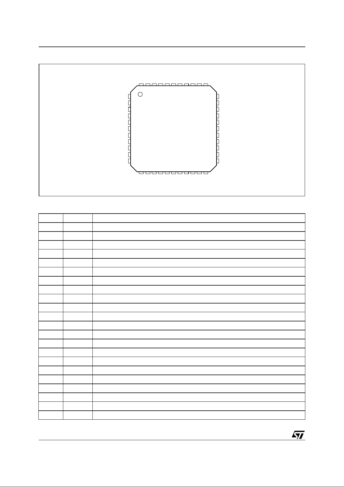
TQFP44
ORDERING NUMBER: STA001
HSB2 High Speed Bipolar Technology for one chip solution for the Starman digital satellite radio receiver.
The STA001 is assembled in a TQFP44 package.
The frontend architecture is a double conversion receiver (see block diagram) .
The chip includes all the RF funct ions up to low IF
and manages the signals to and from the baseband.
BLOCK DIAGRAM
AGC1, AGC2
CE
VCO
:363.625- 373.75
I2CBUS INTERFACE
RF MIXER
1338.14 - 1375.4 MHz 117.0806 MHz
1st PLL
CHARGE
PUMP
SCL SDA
PHASE
DETECTOR
V
V
LNI, NLNI
TK1,
NTK1
ENRFOSC
V
V
DD1
SS1
FLT1
TLCK
DD2
SS2
PADJ1, PADJ2
SUPPLY1 :RF
LNA
LOCK
DETECTOR
SUPPLY2 :PLL1 +
Crystal osc .
CHANNEL SELECTION
November 2002
This is preliminary information on a new product now in development. Details are subject to change without notice.
SIP, SIN
IF1 BUFFER
SOP, SON
3.68MHz
:4
113.23KHz
:130
XOSEL
VGA
MUX
IF1 to IF2 MIXER
PHASE
DETECTOR
2nd PLL
OSC
REF
GADJ1, GADJ2
BUFFER
XTAL1, XTAL2
IF2 BUFFER
CHARGE
PUMP
: 1034
14.72MHz
SUPPLY4 :IF1,
IF2 &PLL2
VCO
SUPPLY3 :DIG.
V
DD4
V
SS4
RXI, NRXI
1.8366 Mhz
FLT2
TK2, NTK2
DIFFERENTIAL
SINGLE ENDED
M_CLK
VDD3
V
SS3
1/20
Page 2
STA001
PIN CONNECTION
(Top view)
ENRFOSC
VDD1
SIP
SIN
VSS1
LNI
NLNI
VSS1
N.C.
PADJ1
PADJ2
VDD4
AGC2
AGC1
VSS4
SON
SOP
VSS4
44 43 42 41 3940 38 37 36 35 34
1
2
3
4
5
6
7
8
9
10
12 13 14 15 16
TK1
VDD2
NTK1
VDD2
FLT1
171118 19 20 21 22
VSS2
XTAL1
PIN FUNCTION
N° Pin Function
1 VDD1 Positive supply 1
2 SIP SAW filter input connection
3 SIN SAW filter input connection
4 VSS1 Negative supply 1
5 LNI RF input
6 NLNI RF input
7 VSS1 Negative supply 1
8 NC Not connected
9 PADJ1 RF gain adjust connection 1
10 PADJ2 RF gain adjust connection 2
11 ENRFOSC RF Oscillator enable
12 VDD2 Positive supply 2
13 TK1 1st PLL tank connection 1
14 NTK1 1st PLL tank connection 2
15 VDD2 Positive supply 2
16 FLT1 1st PLL loop filter connection
17 VSS2 Negative supply 2
18 XTAL1 Quartz oscillator connection 1
19 XTAL2 Quartz oscillator connection 2
20 REF External optional TCXO input
21 XOSEL Internal/external XO selection
22 TLCK Lock detector output
TK2
NTK2
REF
XTAL2
FLT2
VDD4
TLCK
XOSEL
33
RXI
32
NRXI
31
GADJ1
30
GADJ2
29
CE
28
VDD3
27
SCL
26
SDA
25
VSS3
24
M_CLK1
23
M_CLK2
D97AU602
2/20
Page 3
STA001
PIN FUNCTION
(continued)
N° Pin Function
23 M_CLK2 Master clock differential output 1
24 M_CLK1 Master clock differential output 2
25 VSS3 Negative supply 3
26 SDA Da ta serial input
27 SCL Clock input
28 VDD3 Positive supply 3
29 CE Chip Enable
30 GADJ2 IF gain adjust connection 2
31 GADJ1 IF gain adjust connection 1
32 NRXI Low IF Signal output 2
33 RXI Low IF Signal output 1
34 FLT2 2nd PLL loop filter connection
35 VDD4 Positive supply 4
36 TK2 2nd PLL tank connection
37 NTK2 2nd PLL tank connection
38 VDD4 Positive supply 4
39 AGC2 VGA control pin 2
40 AGC1 VGA control pin 1
41 VSS4 Negative supply 4
42 SON SAW filter output connection
43 SOP SAW filter output connection
44 VSS4 Negative supply 4
ABSOLUTE MAXIMUM RATINGS
Symbol Parameter Value Unit
T
T
V
V
V
VDD
V
stg
oper
max
min
maxi
esd
Storage temperature -40 , +125 °C
Operative ambient temperature -20 , +85 °C
Maximum voltage on any pin (with the exception of CE, SDA, SDL)
VDD+0.3 V
Minimum voltage on any pin GND-0.3 V
Maximum voltage on pins CE, SDA, SDL VDD+0.6 V
Minimum/Maximum power supply between VDD
max
VSS
1,2,3,4
1,2,3,4
and
-0.3/5.5 V
Electrostatic Discharge Voltage (ESD) 2 KV
OPERATING CONDITIONS
Symbol Parameter Value Unit
VDD Opera ting voltage 2.7, 3.3 V
T
jun
Junction temperature -30, +95 °C
3/20
Page 4
STA001
THERMA L D ATA
Symbol Parameter Value Unit
R
Th j-amb
(1) According to JEDEC specific ation on a 4 layers board
Thermal Resistance Junction to Ambient
(1)
45 °C/W
ELECTRICAL CHARACTERISTCS
Symbol Parameter Test Condition Min. Typ. Max. Unit
SUPPLY CURRENTS (T
I
CC1
Current supplied by
VDD1
CC2
Current supplied by
I
VDD2
I
CC3
Current supplied by
VDD3
= 25°, VDD = 3V)
amb
Powered circuits: LNA, RF mixer, IF buffer 9.5 14 17 mA
Powered circuits: RF pll, Crystal Oscillator.
ENRFOSC=high (IC RF Osc. Enabled),
8.5
10
12
XOSEL=high (IC XO Enabled)
ENRFOSC=low (IC RF Osc. Disabled),
3
5
6
XOSEL=high (IC XO Enabled)
ENRFOSC=high (IC RF Osc. Enabled),
7.5
9
11
XOSEL=low (IC XO Disabled)
ENRFOSC=low (IC RF Osc. Disabled),
2
4
5
XOSEL=low (IC XO Disabled)
Powered circuits: Digital cells 12 15 18 mA
mA
mA
mA
mA
I
CC4
Current supplied by
VDD4
Powered circuits: VGA, IF mixer, output
buffer, IF pll.
V(AGC1)=V(AGC2)=1.2 (IF
I
TOTICC1
+ I
CC2
+ I
CC3
+ I
ENRFOSC=high (IC RF Osc. Enabled),
CC4
XOSEL=high (IC XO Enabled)
ENRFOSC=low (IC RF Osc. Disabled),
XOSEL=high (IC XO Enabled)
ENRFOSC=high (IC RF Osc. Enabled),
XOSEL=low (IC XO Disabled)
ENRFOSC=low (IC RF Osc. Disabled),
XOSEL=low (IC XO Disabled)
I
TOTSB
Standby I
I
+ I
CC3
CC4
CC1
+ I
CC2
+
CE=GND 100 µA
LNA, RF MIXER AND IF1 BUFFER (T = 25°, VDD-VSS = 3V)
BW
BW
Input signal BW 1452 1492 MHz
i
Output signal BW 114 116.5 MHz
o
G
Voltage Gain Input LNI, NLNI pins; output SIP, NIP pins.
V
= 200Ω, PADJ1, PADJ2 floating
R
L
gain
=75dB)
71114mA
40
34
39
34
50
45
49
44
61
55
60
54
mA
mA
mA
mA
28 30 33 dB
4/20
Page 5

STA001
ELECTRICAL CHARACTERISTCS
(continued)
Symbol Parameter Test Condition Min. Typ. Max. Unit
G
Minimum Voltage Gain Input LNI, NLNI pins; output SIP, NIP pins.
Vtrim
Z
Input impedance R || C Balanced, LNI, NLNI pins 75
i
= 200Ω, R
R
L
ext
=0
22 25 28 dB
0.2
Output impedance Balanced, SIP, SIN pins 50 Ω
Z
o
R
Input Return Loss LNI, NLNI pins 14 dB
l
IIP3 Input IP3 Input LNI, NLNI pins; output SIP, NIP pins,
R
=200Ω, PADJ1, PADJ2 floating
l
IIP3
1dBcp Input 1 dB compression
1dBcp
Input IP3 minimum gain Input LNI, NLNI pins; output SIP, NIP pins,
trim
=200Ω, R
R
l
=0 on PADJ1, PADJ2
ext
Input LNI, NLNI pins; output SIP, NIP pins,
point
Input 1 dB compression
tri
m
point
R
=200Ω, PADJ1, PADJ2 floating
l
Input LNI, NLNI pins; output SIP, NIP pins,
=200Ω, P ADJ1, P ADJ2 R
R
l
=0 on PADJ1,
ext
-20 -15 dBm
-19.5 -11.5 dBm
-26 dBm
-24 dBm
PADJ2
NF Noise figure contribution Measurement conditions: Input LNI, NLNI
5dB
pins; output SIP, NIP pins. Rs=50Ω,
Rl=200Ω, DSB, PADJ1, PADJ2 floating
Ω
pF
NF
IF1
RF
V
Noise figure contribution
trim
minimum gain
LO1 to IF1 leakage -100 -25 dBm
leak
LO1 to RF leakage -100 -30 dBm
leak
LNI, NLNI common mode
DC
Measurement conditions: Input LNI, NLNI
pins; output SIP, NIP pins. R
Rl=200Ω, DSB, R
=0 on PADJ1, PADJ2
ext
=50Ω,
s
AC coupled to the Balun VDD-
DC voltage
V
SIP, SIN common mode
DC
AC coupled to the SAW filter VDD-
DC voltage
IF VGA AMPLIFIER, IF MIXER AND OUTPUT BUFFER (T = 25°, VDD-VSS = 3V)
BW
BW
G
G
I
AGC
Input signal BW 114 116.5 MHz
i
Output signal BW 0.6 3.1 MHz
o
Minimum gain Input LNI, NLNI pins; output SIP, NIP pins.
min
Rl=high impedance V(AGC
Maximum gain Input LNI, NLNI pins; output SIP, NIP pins.
max
Rl=high impedance V(AGC
1,2
1,2
)=0V
)=3V
Input current in AGC
control pin
Z
AGC
AGC pin input
impedance
6.5 dB
VDD-1 VDD-
1.2
1.3
VDD-
1.1
0.8
VDD-
0.9
32 37 dB
71 86 dB
10 µA
600 KΩ
V
V
5/20
Page 6

STA001
ELECTRICAL CHARACTERISTCS
(continued)
Symbol Parameter Test Condition Min. Typ. Max. Unit
NF Noise figure contribution Measurement conditions: Input SIP, NIP
pins; output SOP, NOP pins. R
=50Ω,
s
9dB
Rl=200Ω, DSB, Gain = 65dB
1dBcp Input 1 dB compression
Gain = 65dB -50 dBm
point
1dBcp
Input 1 dB compression
fg
Gain = 81dB -66 dBm
point full gain
IIP3 Input IP3 Gain = 65dB -41 dBm
IIP3
Z
V
V
V
Input IP3 full gain Gain = 81dB -57 dBm
fg
Z
Input impedance Balanced, SOP, SON pins 50 Ω
in
Output impedance Balanced, RXI, NRXI pins (see fig. 9) 200 Ω
out
SOP, SON common
DC
mode DC voltage
RXI, NRXI common
DC
mode DC voltage
GADJ1, GADJ2 common
DC
mode DC voltage
AC coupled to the SAW filter VDD-
1.2
VDD-
2.1
VDD-
0.15
VDD-1 VDD-
0.8
VDD-
1.36
VDD-
V
DD
0.12
V
V
V
Z
Gain adjustment pins
adj
Balanced, GADJ1, GADJ2 pins 800 Ω
impedance
BB
IF2
LO2 to BB leakage Obtained using low pass filter at the output -45 dBm
leak
LO2 to IF2 leakage Obtained with SAW filter connected to IF
leak
port
IM3 Third order IM product V
out
=1V
DDp
Figure 1. Typical IF Overall Gain vs Control Voltage
IF TOTAL VOLTAGE GAIN (dB)
input SOP,NOP output RXI,NRXI
60
55
50
45
40
IF TOTAL VOLTAGE GAIN (dB)
35
30
0.7 0.75 0.77 0.79 0.8 0.82 0.84 0.86 0.88 0.9
V(AGC1, AGC2) (Volt)
IF gain (dB)
-100 -30 dBm
-30 dBc
IF TOTAL VOLTAGE GAIN (dB)
input SOP,NOP output RXI,NRXI
90
85
80
75
70
IF TOTAL VOLTAGE GAIN (dB)
65
60
1
1.2
1.4
1.6
1.1
1.3
1.5
1.8
1.7
1.922.1
V(AGC1, AGC2) (Volt)
IF gain (dB)
2.2
2.4
2.3
2.6
2.5
2.7
6/20
Page 7

STA001
ELECTRICAL CHARACTERISTCS
(continued)
Symbol Parameter Test Condition Min. Typ. Max. Unit
CRYSTAL OSCILLATOR (T = 25°, VDD-VSS = 3V)
V
XTAL1, XTAL2 common
DC
mode DC voltage
XOSEL high VDD-
1.1
VDD-
0.68
PLLs, SYNTHESIZERS (T = 25°, VDD-VSS = 3V)
t
RF pll loop settling time within 1 KHz final freq. Offset, by using the
s
1ms
loop filter of Application board
P
Total phase noise
n
contribution
f
REF1
RF pll comparation
100Hz < ∆f < 1.84Mhz,
Q
rf_tank
≥20, Q
if_tank
≥20
1.6 deg
3.68 MHz
frequency
f
REF2
IF pll comparation
113.23 KHz
frequency
P
N
prog1
Spurious power level*** RF pll, ∆fc=n*460KHz n=1,2..
SP
IF pll, ∆fc=113.23KHz
RF PLL selectable
division ratios
from REF1 to LO1, range covered by a 0.5
step, using a 14.72MHz quartz
-100
1443
(first
used
1454.5)
-50
-45
1506.5
(last
used
1495)
V
rms
dBc
dBc
N
prog2
RF PLL selectable
division ratios
N
N
REF1
N
REF2
*** Using l oop filter as s uggested in application board schematics
IF PLL fixed division ratios from REF2 to LO2, 1 fixed +2 testing values
fix
REF1 division ratio from Crystal oscillator to REF1 4
REF2 division ratio from Crystal oscillator to REF2 130
from REF1 to LO1, range covered by a 0.5
step, using a 14.725MHz quartz
RF VCO (T = 25°, VDD-VSS = 3V)
f
LO1_1
f
LO1_2
V
FLT1
LO Freq. range Using 14.72Mhz quartz
LO Freq. range Using 14.725Mhz quartz
Freq. control voltage
Pin FLT1
range
V
TK1, NTK1 DC voltage ENRFOSC high VDD-
DC
Input impedance R || C Balanced, TK1, NTK1 pins 300
Z
i
1443
(first
used
1454)
1506.5
(last
used
1494.5)
987 1034 1081
1338.14
1375.4 MHz
1338.134375 to 1375.407031
V
SS
0.2
1.3
+
VDD-
1.1
VDD -
0.2
VDD-
0.65
0.2
MHz
V
V
Ω
pF
7/20
Page 8

STA001
ELECTRICAL CHARACTERISTCS
(continued)
Symbol Parameter Test Condition Min. Typ. Max. Unit
IF VCO (T = 25°, VDD-VSS = 3V)
f
LO2_1
LO Freq. Using a 14.72MHz quartz, Min. and Max.
111.76 117.08 122.4 MHz
Values are optional fixed frequency usable
for testing purposes.
f
LO2_2
LO Freq. Using a 14.725MHz quartz, Min. and Max.
111.8 117.12 122.44 MHz
Values are optional fixed frequency usable
for testing purposes.
V
FLT2
Freq. control voltage
range
FLT2 pin VSS +
0.2
VDD -
0.2
DIGITAL INTERFACE TO MP (SCL, SDA, TLCK) AND XOSEL INTERFACE (T = 25°, VDD-VSS = 3V)
INPUT PARAMETERS (SCL, SDA)
V
V
digital input signals high VDD-1 V
IH
IL
Input current High 10 µA
I
IH
I
Input current Low -40 µA
IL
low V
SS
DD
VSS+0.7V
V
V
T
Input edge transition 0.1 µs/V
t
R
Input resistance 190K Ω
in
OUTPUT PARAMETERS (TLCK)
V
V
digital output signals high VDD-
OH
OL
Rise time Cl=5pF 0.4 µs/V
t
r
t
Fall time Cl=5pF 0.4 µs/V
f
low V
DIFFERENTIAL DIGITAL INTERFACE (M_CLK1, M_CLK2) (T = 25°, VDD-VSS = 3V)
V
digital output signals,
OH
high 0.2 V
V(M_CLK1) -
V
V
V(M_CLK2)
OL
M_CLK1, M_CLK2
DC
common mode DC voltage
Rise time Cl=5pF each pin 10 ns
t
r
t
Fall time Cl=5pF each pin 10 ns
f
low -0.2 V
VDD-
1.12
0.5
SS
V
DD
VSS+0.5V
VDD-
0.7
V
V
8/20
Z
Output impedance balanced 500 Ω
out
Page 9

STA001
ELECTRICAL CHARACTERISTCS
(continued)
Symbol Parameter Test Condition Min. Typ. Max. Unit
f
M_CLK1
f
M_CLK2
M_CLK frequency Using a 14.72MHz quartz 14.72 MHz
M_CLK frequency Using a 14.725MHz quartz 14.725 MHz
ADDITIONAL DIGITAL INTERFACE (CE) (T = 25°, VDD-VSS = 3V)
(LOW=GND, HIGH=VDD)
V
digital input signals high
IH
VSS+1.
8
V
IL
CE power up time 2 µs
t
r
t
CE power down time 6 µs
f
low
VSS+1.3V
XOSEL, CE, TLCK, ENRFOSC TRUTH TABLE (LOW = GND, HIGH = VDD)
Pin Type Level Result
CE inp ut high Chip enabled
low Chip disabled
V
XOSEL input high Internal Crystal oscillator selected
low External TCXO connected on REF selected
ENRFOSC input high Internal RF oscillator selected
low External RF oscillator connected on TK1, NTK1 pins
TLCK output high Synth. locked
low Synth. unlocked
ADDITIONAL OPTIONAL INTERFACE INFORMATION (REF)
Symbol Parameter Test Condition Min. Typ. Max. Unit
V
REF DC voltage XOSEL low VDD-
DC
1.1
R
Input resistance XOSEL low 70K Ω
in
VDD-
0.9
VDD-
0.7
V
9/20
Page 10

STA001
FUNC TIONAL DESCRIPTION
Receiver chain
The receiver chain transforms the RF frequency signals to an IF signal at 1.84 MHz Carrier directly usable by
the Channel decoder.
In front of the STA001 IC it can be placed an external LNA and a bandpass filter; the bandpass filter limitates
the input bandwidth and guarantees a suitable rejection to the image frequency.
The STA001 input stage is a LNA working in the 1452-1492 MHz band . The RF signal is downconverted, using
an active mixer, to a first IF of 115.244 MHz. The first LO is tunable with a frequency step of 460 KHz.
The RF can be reduced 5dB by an external trimmer/resistor connected between PADJ1 and PADJ2 pins.
An IF variable gain amplifier guarantees 54 dB typical of gain range.
Using pins GADJ1, GADJ2, the output RX signal level can be decreased to the desired val ue by an external
trimmer/resistor.
Moreover, the IF chain can be configured to have a fixed gain by fixing statically control voltages on AGC1 and
AGC2 pins (i.e. V(AGC1)=VCC and V(AGC2)=GND), and by trimming the gain through connecting an external
resistor between GADJ1 and GADJ2.
By using an 800 Ohm resistor connected between GADJ1 and GADJ2, for example, a typical 56 dBs IF static
gain is obtained.
The first IF si gnal, having a bandwidth of 2.5 MHz, shaped by an external SAW filter , is downconverted to a
second IF of 1.84 MHz.
A differential clock output at 14.72 MHz is available to be used from the baseband.
Synthesizers, PLL, charge pump and VCOs
The first Voltage controlled Oscillator is controlled by an integrated PLL and it's able to cover a frequency range
of 37MHz with a step size of 460 KHz.
The second Voltage controlled oscillator produces a fixed 117.08MHz frequency controlled by a second integrated PLL. Moreover, the 2nd PLL is able to select 2 other fixed frequencies, i.e. 111.76MHz and 122.4MHz,
suitable for application test.
The other components of the first PLL sy nthesizer are a low frequency programmable divider and a dual m odulus prescaler; a fixed dividers is ins tead used to synthesize the second VCO frequency. Other fixed internal
dividers are used to get the comparation frequencies of both loops.
Channel selection is made through the I
2
CBUS interface , directly from the µP.
POWER SUPPLIES
The chip operates from an unregulated power supply of 2.7 to 3. 3 Volts . All i nt erface circui ts to t he baseband
chips are operating between these supplies unless otherwise specified.
INTERFACE SPECIFICATION
All the interface voltage levels to the micro controller are referenced to the supply voltage of the interface power
supply (GND) . The interface voltage levels are therefore fully compatible with the base band circuits.
The digital levels are all CMOS threshold compatible with the exception of M_CLK 1, M _CLK2 pins (ECL type).
For completeness all other interface signals are also included.
I2C BUS INTERFACE
Data transmission from m icroproce ssor to the STA001 takes place through the 2 wires I2C BUS interface, consisting
of the two lines SDA and SCL (pull-up resistors to positive supply voltage must be connected to SDA and SCL).
10/20
Page 11

STA001
Data Validity
The data on the SDA line must be stable during the high period of the clock. The HIGH to LOW state of the data
line can only change when the clock signal on the SCL line is LOW.
Start and Stop conditions
A start condition is a HIGH to LOW transition of the SDA line while SCL is HIGH. The stop condition is a LOW
to HIGH transition of the SDA line while SCL is HIGH.
Byte format
Every byte transferred on the SDA line must contains bits. Each byte must be followed by an acknowledge bit.
The MSB is transferred first.
Acknowledge
The master (µP) puts a resistive HIGH level on the SDA line during the acknowledge clock pulse. The peripheral
(STA001) that acknowledges has to pull-down (LOW) the SDA line during the clock pulse.
The STA001 which has been addressed has to generate an acknowledge after the reception of each byte, otherwise the SDA line remains at at the HIGH level during the ninth clock pulse time. In this case the
erate the STOP information in order to abort the transfer.
µ
P can gen-
Transmission without acknwoledge
Avoiding to detect the acknowlegde of the STA001, the µP can use a simpler transmission: simply it waits one
clock period without checking the STA001 acknowledging, and sends the new data.
This approach of course is less protected from misworking.
Figure 2. Vali di ty on the I2CBUS
SDA
SCL
DATA LINE
STABLE, DATA
Figure 3. Timin g D i agram of the I
SCL
SDA
VALID
2
CBUS
CHANGE
DATA
ALLOWED
D99AU1031
2
CBUS
I
START
D99AU1032
STOP
11/20
Page 12

STA001
Figure 4. Ackn owl e d ge on the I2CBUS
SCL
SDA
START
TIMING SPECIFICATION
Figure 5. Dat a and clock
SDA
SCL
Symbol Parameter Minimum time (ns)
t
cs
t
ch
t
cwh
t
cwl
1
MSB
t
cs
23789
D99AU1033
t
cwl
t
ch
Data to clock set up time 100
Data to clock hold time 50
Clock pulse width high 100
Clock pulse width low 100
t
cwh
ACKNOWLEDGMENT
FROM RECEIVER
Figure 6. Start and stop
SDA
SCL
Symbol Parameter Minimum time (ns)
Tstart
1,2
Tstop
1,2
12/20
t
t
stop1
t
t
start1
start2
Clock to data start time 100
Data to clock down stop time 100
stop2
Page 13

Figure 7.
STA001
SDA
SCL
Symbol Parameter Maximum time (ns)
t
d1
t
d2
Ack begin delay 200
Ack end delay 200
89
td1
td2
SOFTWARE SPECIFICATION
Interface protocol
The interface protocol comprises:
- A start condition (S)
- A chip address byte
- A two data bytes
- A stop condition (P)
MSB chip address LSB MSB 1st data byte LSB MSB 2nd data byte LSB
S11000000
1 D6D5D4D3D2D1D0
ack
0 D6D5D4D3D2D1D0ack P
ack
ack = Acknowledge
S = Start
P = Stop
"Byte by byte" option
A "byte by byte" programming mode is also possible when there is no need to use both data bytes to program
the chip (for example during the setup of 2nd PLL).
To use this feature remember that first bit of both data bytes is reserved to chose the destination of the remaining
7 bits.
MSB chip address LSB MSB 1st data byte LSB
ack
S11000000
K D6D5D4D3D2D1D0ack P
ack = Acknowledge
S = Start
13/20
Page 14

STA001
P = Stop
K= destination of the remaining 7bit:
K=1 the data byte has the same function of the 1st data byte in the normal programming mode.
K=0 the data byte has the same function of the 2nd data byte in the normal programming mode.
Table 1. First data byte selection table (selection of synthesizer channel) using a 14.72Mhz quartz
Division ratio
MSB LSB RF LO freq. selected Units
selected on
synthesizer
Notes
D6 D5 D4 D3 D2 D1 D0
0 0 0 0 1 1 0 1324.8+6*0.46
(1327.56)
0 0 0 0 1 1 1 1324.8+7*0.46 MHz 360.875
0 0 0 1 0 0 0 1324.8 + 8*0.46 MHz 361
-------
0 0 1 1 1 0 1 1338.14 MHz 363.625 first used freq.
- - - - - - - 1324.8 + N*0.46
N=(D6..D0)
represented decimal
number
1 1 0 1 1 1 0 1375.4 MHz 373.75 Last used freq.
-------
1 1 1 1 1 1 1 1383.22 MHz 375.875
0 0 0 0 0 0 0 1383.68 MHz 376
-------
0 0 0 0 1 0 1 1324.8+133*0.46
(1385.98)
MHz 360.75 Lowest
MHz 360 + N*0.125 general freq.
MHz 376.625 Highest
from REF1 to
LO1
selectable freq.
generation rule
selectable freq.
1 0 0 0 1 0 1 1356.54 MHz 368.625 Startup
presetted data
14/20
Page 15

STA001
Table 2. First data byte selection table (selection of synthesizer channel) using a 14.725Mhz quartz
MSB LSB RF LO freq. selected Units
D6 D5 D4 D3 D2 D1 D0 from REF1 to
0 0 0 0 1 1 0 1325.25 +6*0.46015625
(1328.010938)
0 0 0 0 1 1 1 1325.25 +7*0.46015625 MHz 360.875
0 0 0 1 0 0 0 1325.25+ 8*0.46015625 MHz 361
-------
0 0 1 1 1 0 0 1338.134375 MHz 363.5 first used freq.
- - - - - - - 1325.25+
N*0.46015625
N=(D6..D0) represented
decimal number
1 1 0 1 1 0 1 1375.407031 MHz 373.625 Last used freq.
-------
1 1 1 1 1 1 0 1383.229688 MHz 375.75
1 1 1 1 1 1 1 1383.689844 MHz 375.875
-------
0 0 0 0 1 0 1 1325.25
+133*0.46015625
(1386.450781)
1 0 0 0 1 0 1 1357.000781 MHz 368.625 Startup
MHz 360.75 Lowest
MHz 360 + N*0.125 general freq.
MHz 376.625 Highest
Division ratio
selected on
synthesizer
LO1
Notes
selectable
freq.
generation
rule
selectable
freq.
presetted data
Table 3. Second data byte selection table (LOCK test on both pll, dividers test and IF pll test)
MSB LSB
D6 D5 D4 D3 D2 D1 D0
0000000 Lock test on RF plllock flag to be tested: TLCK;
0000100 Lock test on IF pll lock flag to be tested: TLCK
0000001Lock test on RF and IF pll lock flag to be tested: TLCK
0010010First pll programmable
0011010First pll reference divider
0010110Second pll fixed divider
0011110Second pll reference
1000000Test frequency on IF pll
1100000Test frequency on IF pll
Working mode Notes
Startup presetted data
output freq. divided by 16
divider test
test
test
divider test
divider by 1034
divider by 1034
available on TLCK
output freq. divided by 8
available on TLCK
output freq. divided by 2
available on TLCK
output freq. available on TLCK
Division ratio changed to 987
Division ratio changed to 1081
15/20
Page 16

STA001
TEST AND APPLICATION BOARD SCHEMATIC
Figure 8. Tes t Bo ard S c hem atic Diagram
CE
CE
R9 1K
R9 1K
R9 1K
RXI OUT
RXI OUT
RXI OUT
J3
J3
J3
1
1
1
C9 220nF
C9 220nF
VCC
VCC
VCC
L2
68nH
L2
68nH
L2
68nH
D2
C1
680pF
D2
D2
C1
680pF
C1
680pF
VCC
VCC
VCC
L1
68nH
D1
L1
68nH
L1
68nH
D1
D1
R2
R2
R2
C3
C3
100nF
100nF
R1
100K
R1
100K
R1
100K
R6
18 k
R6
18 k
R6
18 k
330pF
330pF
330pF
3.3 nF
3.3 nF
3.3 nF
C5
C7
C5
C5
C7
C7
R5
R5
R5
5.6 K
5.6 K
5.6 K
MA372J
MA372J
MA372J
MA372J
MA372J
MA372J
C6
C6
100nF
100nF
100K
100K
NRXI OUT
NRXI OUT
NRXI OUT
SMA
SMA
SMA
SMA
SMA
2
2
2
2
2
1
1
C11 220nF
C11 220nF
C11 220nF
VP4b
VP4a
VP4b
VP4b
VP4a
FLT2
FLT2
FLT2
34
34
34
VP4
VP4
VP4
35
35
35
TK2
TK2
TK2
36
36
36
NTK2
NTK2
NTK2
37
37
37
VP4
VP4
VP4
38
38
38
AGC2
AGC2
AGC2
39
39
39
AGC1
AGC1
AGC1
40
40
40
VN4
VN4
VN4
41
41
41
SON
SON
SON
42
42
42
SOP
SOP
SOP
43
43
43
VN4
VN4
VN4
44
44
44
U1
U1
U1
C15
C15
C15
J4
J4
SCL
SCL
SCL
R8
R8
R8
VP3
VP3
VP3
3332313029282726252423
3332313029282726252423
3332313029282726252423
CE
CE
CE
RXI
RXI
RXI
VP3
VP3
VP3
SCL
SCL
SCL
NRXI
NRXI
NRXI
GADJ1
GADJ2
GADJ1
GADJ2
GADJ1
GADJ2
STA001
STA001
STA001
VP1
SIP
SIN
VN1
LNI
NLNI
VN1NCPADJ1
VP1
SIP
SIN
VN1
LNI
VP1
SIP
SIN
VN1
LNI
NLNI
VN1NCPADJ1
NLNI
VN1NCPADJ1
123456789
123456789
123456789
VP1
VP1
VP1
10nF
10nF
10nF
SDA
SDA
R12
4.7K
R12
4.7K
R12
4.7K
R11
4.7K
R11
4.7K
VN3
VN3
VN3
SDA
SDA
SDA
M_CLK1
M_CLK2
M_CLK1
M_CLK2
M_CLK1
M_CLK2
PADJ2
ENRFOSC
PADJ2
ENRFOSC
PADJ2
ENRFOSC
10
11
10
11
10
11
JP1
R10
JP1
R10
JP1
R10
1 2
1 2
1 2
CLK1
CLK2
CLK1
CLK1
VCC
VCC
VCC
C16 10nF
C16 10nF
C16 10nF
TLCK
TLCK
TLCK
22
22
22
XOSEL
XOSEL
XOSEL
21
21
21
REF
REF
REF
20
20
20
XTAL2
XTAL2
XTAL2
19
19
19
XTAL1
XTAL1
XTAL1
18
18
18
VN2
VN2
VN2
17
17
17
FLT1
FLT1
FLT1
16
16
16
VP2
VP2
VP2
15
15
15
NTK1
NTK1
NTK1
14
14
14
TK1
TK1
TK1
13
13
13
VP2
VP2
VP2
12
12
12
VP2b
VP2a
VP2b
VP2a
VP2b
VP2a
JUMPER2
JUMPER2
JUMPER2
3 4
3 4
3 4
T_LOCK
CLK2
CLK2
T_LOCK
VCC
VCC
VCC
C20 10nF
C20 10nF
C20 10nF
JP2
JP2
JP2
1 2
3 4
1 2
3 4
1 2
3 4
C23
C23
C23
R15
390
R15
390
R15
390
R14
0
R14
0
R14
0
SMA
SMA
SMA
J6
J6
J6
2
2
2
1
1
1
R17
50
R17
50
C28 10nF
C28 10nF
C28 10nF
Y1
Y1
Y1
C27
C27
C27
CRYSTAL
CRYSTAL
CRYSTAL
15nF
15nF
15nF
C24
C24
C24
C29
150nF
C29
150nF
C29
150nF
C30
C30
C2 1nF
C2 1nF
C2 1nF
T1
T1
1 245 6 R4
1 245 6 R4
1
1
1
J1
J1
J1
IF2 IN
IF2 IN
IF2 IN
AGC1
AGC1
AGC1
C8 1nF
C4 1nF
C4 1nF
C4 1nF
1:1
1:1
1:1
NEOSID 553 200
NEOSID 553 200
R3
50
R3
50
R3
50
SMA
SMA
SMA
2
2
2
C8 1nF
C8 1nF
T2
T2
T2
1 245 6
1 245 6
1 245 6
1
1
1
J2
J2
J2
C10 1nF
C10 1nF
C10 1nF
1:4
1:4
1:4
NEOSID 553 210
NEOSID 553 210
NEOSID 553 210
R7
50
R7
50
SMA
SMA
SMA
2
2
2
IF1 OUT
IF1 OUT
IF1 OUT
C13 8pF
C13 8pF
C13 8pF
T3
T3
T3
1 245 6
1 245 6
1 245 6
C12
C12
C12
1
1
1
J5
J5
J5
RF IN
RF IN
RF IN
VCC
VCC
VCC
L4 1nH
L4 1nH
C14 8pF
C14 8pF
C14 8pF
1:1
1:1
1:1
LDB20C500A1500
LDB20C500A1500
LDB20C500A1500
L3
L3
L3
SMA
SMA
SMA
2
2
2
D3
D3
C17 8pF
C17 8pF
C17 8pF
R13 1 K
R13 1 K
VCC
VCC
VCC
VCC
VCC
C19 100pF
C19 100pF
C19 100pF
HVU355
HVU355
HVU355
HVU355
HVU355
D4
D4
D4
VCC
VCC
VCC
VCC
VCC
C22 100pF
C26 100pF
C22 100pF
C26 100pF
C22 100pF
C26 100pF
L5 1nH
C37 8pF
L5 1nH
L5 1nH
C378pF
C37 8pF
R16 1 K
R16 1 K
R16 1 K
10uF
10uF
+ C31
+ C31
C36
100nF
C36
100nF
C36
100nF
C35
1nF
C35
1nF
C34
8pF
C34
8pF
VCC
VCC
VCC
C33 100pF
C33 100pF
C33 100pF
VCC
VCC
VCC
VCC
VCC
VCC
C41 100pF
C39 100pF
C41 100pF
C41 100pF
C39 100pF
C39 100pF
AGC2
AGC2
AGC2
NOTE: Connect a resis to r from10K to 100K between pi ns PADJ1 (9) and PADJ2 (1 0) so to obtain intermediate gain between 25 and 30dB
16/20
Page 17

Figure 9. Application Board Schematic Diagram
X
O
X
X
O
O
STA001
SMA
SMA
SMA
2
2
2
FLT2
FLT2
FLT2
VP4
VP4
VP4
TK2
TK2
TK2
NTK2
NTK2
NTK2
VP4
VP4
VP4
AGC2
AGC2
AGC2
AGC1
AGC1
AGC1
VN4
VN4
VN4
SON
SON
SON
SOP
SOP
SOP
VN4
VN4
VN4
U2
U2
U2
NR
NR
NR
SMA
SMA
SMA
2
2
2
J2
J2
J2
1
1
1
SDA
SCL
SDA
SDA
SCL
SCL
C9 150nF
C9 150nF
C9 150nF
VP3
VP3
VP3
VCC
VCC
VCC
3332313029282726252423
3332313029282726252423
3332313029282726252423
CE
CE
CE
RXI
RXI
RXI
VP3
VP3
VP3
SCL
SCL
SCL
SDA
SDA
SDA
NRXI
NRXI
NRXI
GADJ1
GADJ2
GADJ1
GADJ2
GADJ1
GADJ2
STA001
STA001
STA001
VP1
SIP
SIN
VN1
LNI
NLNI
VN1NCPADJ1
VP1
SIP
SIN
VN1
LNI
NLNI
VN1NCPADJ1
VP1
SIP
SIN
VN1
LNI
NLNI
VN1NCPADJ1
123456789
123456789
123456789
VP1
VP1
VP1
C14 8pF
C16 8pFL6
C14 8pF
C16 8pFL6
C14 8pF
C16 8pFL6
T1
T1
T1
1 245 6
1 245 6
1 245 6
C15
2.2p
C15
2.2p
C15
2.2p
C13
6.8p
C13
6.8p
C13
6.8p
CLK1
CLK2
CLK1
CLK1
R7
4.7K
R7
4.7K
R7
4.7K
R6
4.7K
R6
4.7K
R6
4.7K
VN3
VN3
VN3
M_CLK1
M_CLK2
M_CLK1
M_CLK2
M_CLK1
M_CLK2
TLCK
TLCK
TLCK
XOSEL
XOSEL
XOSEL
REF
REF
REF
XTAL2
XTAL2
XTAL2
XTAL1
XTAL1
XTAL1
VN2
VN2
VN2
FLT1
FLT1
FLT1
VP2
VP2
VP2
NTK1
NTK1
NTK1
TK1
TK1
TK1
VP2
VP2
VP2
PADJ2
ENRFOSC
PADJ2
ENRFOSC
PADJ2
ENRFOSC
10
11
10
11
10
11
VCC
VCC
VCC
1:1
1:1
1:1
LDB20C500 A1500
LDB20C500 A1500
LDB20C500 A1 500
L8
6.8nH
L8
6.8nH
L8
6.8nH
C20 10nF
C20 10nF
C20 10nF
VCC
VCC
22
22
22
21
21
21
20
20
20
19
19
19
18
18
18
17
17
17
16
16
16
15
15
15
14
14
14
13
13
13
12
12
12
VP2a
VP2b
VP2a
VP2a
VP2b
VP2b
L9 2.2nH
L9 2.2nH
L9 2.2nH
C19 8 p F
C19 8 p F
C19 8 p F
T_LO CK
CLK2
CLK2
T_LO CK
T_LO CK
C21 10nF
C21 10nF
C21 10nF
VCC
VCC
VCC
Y1
Y1
Y1
C23
C23
C23
C26
C26
C26
CRYSTAL
CRYSTAL
CRYSTAL
15nF
15nF
15nF
C24
C24
C24
C27
R10
R10
R10
R9
R9
R9
HVC355B
HVC355B
HVC355B
D3
D3
D3
R8 1K
R8 1K
R8 1K
150nF
390
C27
150nF
C27
150nF
390
390
0
0
0
C28
C28
C28
HVC355B
HVC355B
HVC355B
D4
D4
D4
L10 2 .2nH
C31 8 p F
L10 2 .2nH
L10 2 .2nH
C31 8 p F
C31 8 p F
R11 1K
R11 1K
R11 1K
RXI
RXI
RXI
J1
J1
J1
1
1
1
C7 150nF
C7 150nF
C7 150nF
VCC
VCC
VCC
L2
68nH
L2
68nH
L2
68nH
C1
680pF
D2
C1
680pF
C1
680pF
D2
VCC
VCC
VCC
AGC
AGC
AGC
R1
10K
R1
10K
R1
10K
10
10
10
11
11
11
12
12
12
13
13
13
14
14
14
15
15
15
16
16
16
17
17
17
18
18
18
D2
D1
L1
68nH
D1
D1
L1
68nH
L1
68nH
U1
U1
U1
GND
GND
GND
GND
GND
GND
OUT
OUT
OUT
NC
NC
NC
NC
NC
OUT
OUT
OUT
NC
GND
GND
GND
GND
GND
GND
GND
GND
GND
GND
GND
GND
GND
GND
GND
GND
GND
GND
IN
IN
IN
NC
NC
NC
IN
IN
IN
NC
NC
NC
S+M Y012B
S+M Y012B
S+M Y012B
GND
GND
GND
GND
GND
GND
L3
L3
L3
R3
18 k
R3
18 k
R3
18 k
330pF
330pF
330pF
3.3 nF
3.3 nF
3.3 nF
C4
C3
C4
C4
C3
C3
R2
R2
R2
5.6 K
5.6 K
5.6 K
VP4b
VP4a
VP4b
VP4b
VP4a
VP4a
MA2S372
MA2S372
MA2S372
MA2S372
MA2S372
MA2S372
C2
C2
C2
100nF
100nF
100nF
9
9
9
8
8
8
7
7
7
6
6
6
5
5
5
4
4
4
3
3
3
2
2
2
1
1
1
100nH
100nH
100nH
34
34
34
35
35
35
36
36
36
37
37
37
38
38
38
39
39
39
40
40
40
41
41
41
42
42
42
43
43
43
44
44
44
L4
56nH
Q1
56nH
56nH
33K
33K
33K
C12
C12
C12
IO
IO
IO
3 4
3 4
3 4
S+M B69813-N1477-A840
S+M B69813-N1477-A840
S+M B69813-N1477-A840
C11
C11
C11
C10
C10
C10
1
1
1
J3
J3
J3
F IN
F IN
F IN
Q1
Q1
312
312
312
100p
100p
100p
GND
GND
GND
GND
GND
GND
GND
GND
GND
GND
GND
GND
5p
5p
5p
100p
100p
100p
2
2
2
SMA
SMA
SMA
2SC5096
2SC5096
2SC5096
L7
L7
L7
U3
U3
U3
6
6
6
5
5
5
2
2
2
1
1
1
7.5nH
7.5nH
7.5nH
L5
L5
L5
100nH
100nH
100nH
L4
L4
R5
R5
R5
C8
22p
C8
22p
C8
22p
R4
33
R4
33
R4
VCC
VCC
VCC
33
C6
10n
C5
100p
C6
10n
C6
10n
C5
100p
C5
100p
Suggested minimum differential RLoad on RXI and NRXI output 3K
C32
1nF
C32
1nF
C32
VCC
VCC
VCC
ANT + B
ANT + B
ANT + B
100p
100p
100p
C18
C18
C18
C17
10n
C17
10n
C17
10n
VCC
VCC
VCC
100pF
100pF
100pF
C22
C22
C22
VCC
VCC
VCC
VCC
VCC
VCC
100pF
100pF
100pF
C25
C25
C25
1nF
VCC
VCC
VCC
VCC
VCC
VCC
100pF
100pF
100pF
C30
C30
C30
100pF
100pF
100pF
100pF
100pF
100pF
C34
C33
C34
C33
C34
C33
17/20
Page 18

STA001
Application note: the crystal oscillator must have the following features:
Symbol Parameter Test Condition Min. Typ. Max. Unit
CRYSTAL OSCILLATOR (T = 25°, VP-VN = 3V)
f
xtal1
f
xtal2
V
Quartz frequency - Resonance mode: series
- Using a 14.72
Quartz frequency - Resonance mode: series
- using a 14.725 quartz
Phase noise ∆f = 1 KHz -120 -118
P
n
XTAL1, XTAL2 common
DC
XOSEL high VP-1.1 VP-0.9 VP-0.7 V
mode DC voltage
14.72 MHz
14.725 MHz
dBc/Hz
18/20
Page 19

STA001
DIM.
mm inch
MIN. TYP. MAX. MIN. TYP. MAX.
A 1.60 0.063
A1 0.05 0.15 0.002 0.006
A2 1.35 1.40 1.45 0.053 0.055 0.057
B 0.30 0.37 0.45 0.012 0.014 0.018
C 0.09 0.20 0.004 0.008
D 12.00 0.472
D1 10.00 0.394
D3 8.00 0.315
e 0.80 0.031
E 12.00 0.472
E1 10.00 0.394
E3 8.00 0.315
L 0.45 0.60 0.75 0.018 0.024 0.030
L1 1.00 0.039
K 0°(min.), 3.5˚(typ.), 7°(max.)
OUTLINE AND
MECHANICAL DATA
TQFP44 (10 x 10)
D
D1
A1
2333
34
B
44
1
e
22
E
E1
12
11
0.10mm
.004
Seating Plane
B
A
A2
C
L
K
TQFP4410
19/20
Page 20

STA001
Information furnished is believed to be accurate and reliable. However, STMicroelectronics assumes no responsibility for the consequences
of use of such information nor for any infringement of patents or other rights of third parties which may result from its use. No license is granted
by implic ation or otherwise under any patent or patent r i ght s of STMi croelectr oni cs. Spec i fications mentioned i n this publication are subject
to change without notice. This publication supersedes and replaces all information previously supplied. STMicroelectronics product s are not
authorized for use as cri tical comp onents in lif e support devi ces or systems without express written approva l of STMicroel ectronics.
The ST logo is a registered trademark of STMicroelectronics
2002 STMicroelectronics - All Ri ghts Rese rved
Austra lia - Brazil - Canada - Chi na - F i nl and - Franc e - Germany - Hong Kong - In di a - Israel - Ita l y - J apan -Malaysia - Malta - Morocco -
Singap ore - Spain - Sw eden - Switze rl and - Unit ed K i ngdom - United States .
STMicroelectronics GROUP OF COMPANIES
http://www.s t. com
20/20
 Loading...