

Datasheet ST95040M6, ST95040M3TR, ST95040M3, ST95040M1TR, ST95040M1 Datasheet (SGS Thomson Microelectronics)
...Page 1

ST95040
ST95020, ST95010
4K/2K/1K Serial SPI EEPROM with Positive Clock Strobe
June 1998 1/18
1 MILLIONERASE/WRITE CYCLES
40 YEARSDATARETENTION
SINGLE SUPPLYVOLTAGE
– 4.5Vto 5.5V forST950x0
– 2.5Vto 5.5V forST950x0W
SPI BUS COMPATIBLE SERIALINTERFACE
2 MHzCLOCK RATE MAX
BLOCKWRITEPROTECTION
STATUSREGISTER
16 BYTE PAGEMODE
WRITEPROTECT
SELF-TIMEDPROGRAMMINGCYCLE
E.S.D.PROTECTIONGREATERthan 4000V
SUPPORTSPOSITIVECLOCK SPI MODES
DESCRIPTION
The ST950x0 is a family of Electrically Erasable
Programmable Memories (EEPROM) fabricated
with STMicroelectronics’s High EnduranceSingle
Polysilicon CMOS technology. Each memory is
accessed by a simple SPI bus compatible serial
interface. The bus signals are a serial clock input
(C),a serial data input(D) and a serialdata output
(Q).
AI01435B
S
V
CC
ST950x0
HOLD
V
SS
W
Q
C
D
Figure1. Logic Diagram
C Serial Clock
D Serial Data Input
Q Serial Data Output
S Chip Select
W Write Protect
HOLD Hold
V
CC
Supply Voltage
V
SS
Ground
Table1. SignalNames
8
1
SO8 (M)
150mil Width
8
1
PSDIP8 (B)
0.25mm Frame
Page 2
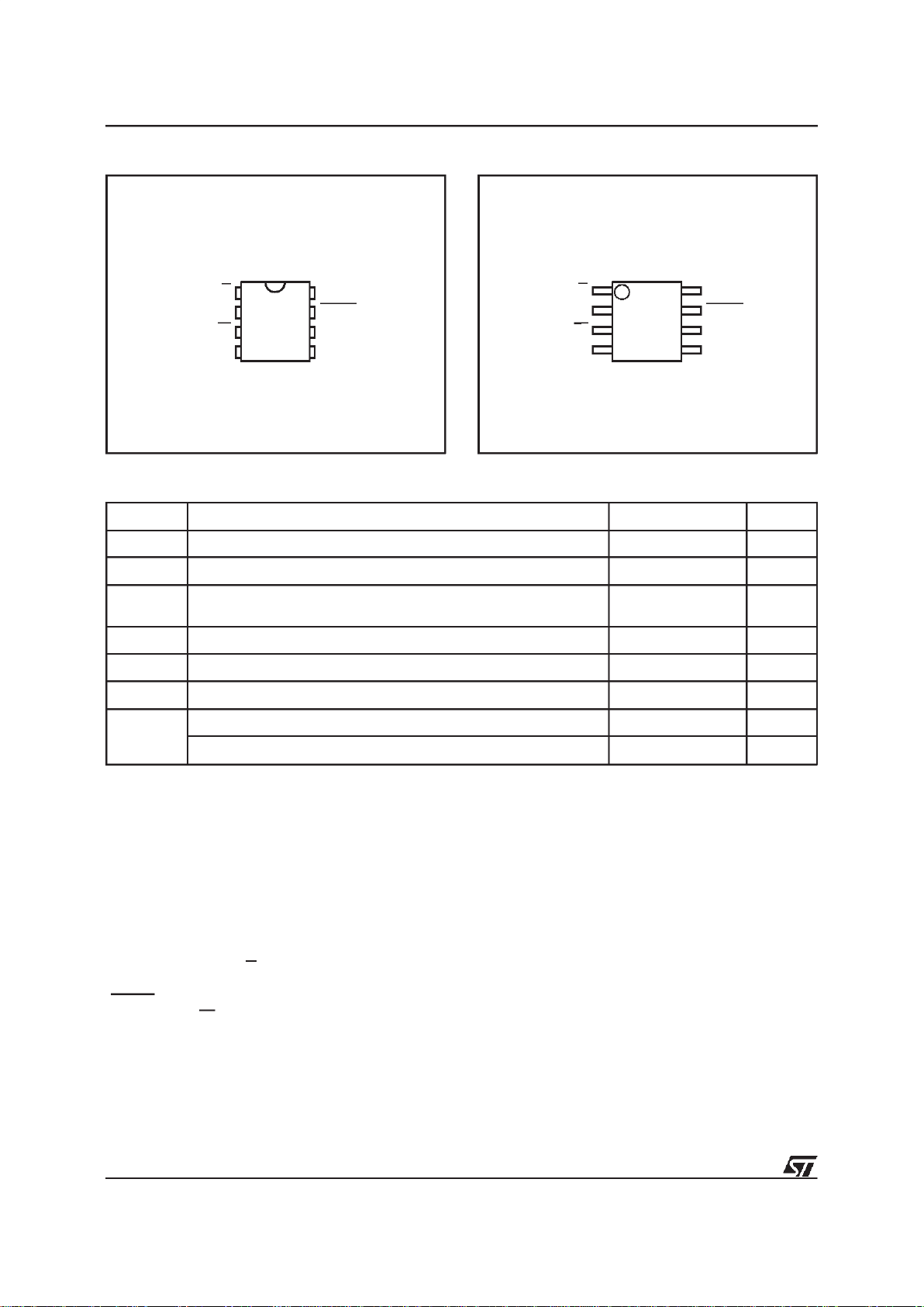
Symbol Parameter Value Unit
T
A
Ambient Operating Temperature –40 to 125 °C
T
STG
Storage Temperature –65 to 150
°
C
T
LEAD
Lead Temperature, Soldering (SO8 package)
(PSDIP8 package)
40 sec
10 sec
215
260
°
C
V
O
Output Voltage –0.3 to VCC+0.6 V
V
I
Input Voltage with respect to Ground –0.3 to 6.5 V
V
CC
Supply Voltage –0.3 to 6.5 V
V
ESD
Electrostatic Discharge Voltage (Human Body model)
(2)
4000 V
Electrostatic Discharge Voltage (Machine model)
(3)
500 V
Notes: 1. Except for the rating ”Operating Temperature Range”, stressesabove those listedin theTable ”Absolute Maximum Ratings”
may cause permanent damage to thedevice. These are stress ratings only and operation of the device at these or any other
conditions above those indicated in the Operating sections of this specification is not implied.Exposure to Absolute Maximum
Rating conditions for extended periods may affectdevice reliability.Refer also to the STMicroelectronics SURE Programand
other relevantquality documents.
2. MIL-STD-883C, 3015.7 (100pF, 1500Ω)
3. EIAJ IC-121 (Condition C) (200pF, 0Ω)
Table2. AbsoluteMaximum Ratings
(1)
Thedevice connectedto the bus is selected when
thechipselectinput(S) goeslow.Communications
with the chip can be interrupted with a holdinput
(HOLD). The write operation is disabled by a write
protectinput (W).
Datais clockedin during the low to high transition
of clock C, data is clocked out during the high to
lowtransitionof clockC.
SIGNALSDESCRIPTION
SerialOutput(Q). Theoutputpin is usedtotrans-
fer data seriallyout of the Memory.Data is shifted
out on the falling edge of theserial clock.
Serial Input (D). The input pin is used to transfer
dataseriallyintothedevice.Itreceivesinstructions,
addresses, and the data to be written. Input is
latchedon the risingedge of the serialclock.
DV
SS
C
HOLDQ
SV
CC
W
AI01436B
ST950x0
1
2
3
4
8
7
6
5
Figure2A. DIPPin Connections
1
AI01437B
2
3
4
8
7
6
5DV
SS
C
HOLDQ
SV
CC
W
ST950x0
Figure2B. SO Pin Connections
DESCRIPTION
(cont’d)
2/18
ST95040, ST95020, ST95010
Page 3
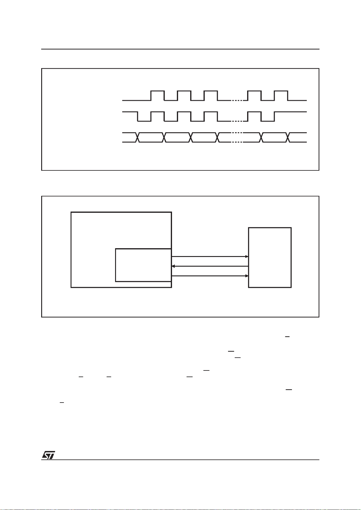
AI01438
C
C
MSB LSB
CPHA
DorQ
0
1
CPOL
0
1
Figure3. Data and Clock Timing
AI01439B
SPI Interface with
(CPOL, CPHA) =
(’0’, ’0’) or (’1’, ’1’)
MICROCONTROLLER
(ST6, ST7, ST9, ST10, OTHERS)
ST95xx0
SCK
SDI
SDO
C
Q
D
Figure4. Microcontrollerand SPI Interface Set-up
Serial Clock (C).
The serial clock provides the
timing of the serial interface. Instructions, addresses,ordatapresentat theinputpinare latched
on the rising edge of the clock input, while data on
theQ pin changesafterthe fallingedgeof theclock
input.
Chip Select (S).
When S is high, the Memory is
deselectedand the Q output pin is at high impedance and, unless an internal write operation is
underwaythe Memorywill bein the standbypower
mode. S low enables the Memory,placingit in the
active power mode. It should be noted that after
power-on,a high to low transition on S is required
priorto the start of any operation.
Write Protect (W).
This pin is for hardwarewrite
protection. When W is low, writes to the Memory
aredisabledbutanyotheroperationsstayenabled.
WhenWishigh,all writesoperationsareavailable.
W going low at any time before the last bit D0 of
thedata streamwillresetthewriteenablelatchand
prevent programming. No action on W or on the
writeenable latchcan interrupta writecycle which
hascommenced.
3/18
ST95040, ST95020, ST95010
Page 4
Hold (HOLD).
The HOLD pin is used to pause
serial communications with the Memory without
resetting the serial sequence. To take the Hold
condition into account, the product must be selected (S = 0). Then the Hold stateis validatedby
a high tolowtransitionon HOLDwhenC islow. To
resumethecommunications,HOLDisbroughthigh
whileC is low.During the Hold conditionD, Q, and
C are at a highimpedancestate.
Whenthe Memoryis underthe Holdcondition,itis
possibletodeselectthedevice.However,theserial
communications will remain paused after a reselect, and the chip will be reset.
TheMemorycanbedrivenbyamicrocontrollerwith
its SPI peripheral running in either of the two followingmodes:(CPOL, CPHA)= (’0’, ’0’)or (CPOL,
CPHA)= (’1’, ’1’).
Forthesetwo modes,inputdatais latchedinby the
lowto high transitionof clockC, andoutputdatais
available from the high to low transition of Clock
(C).
Thedifferencebetween(CPOL, CPHA)=(0,0)and
(CPOL,CPHA) = (1,1) is the stand-bypolarity:C
remains at ’0’ for (CPOL, CPHA) = (0, 0) and C
remainsat’1’for(CPOL,CPHA)=(1,1)whenthere
is no data transfer.
OPERATIONS
All instructions,addresses and data are shifted in
and out of the chip MSB first. Data input (D) is
sampled on the first rising edge of clock (C) after
thechip select(S) goeslow.Priorto any operation,
a one-byte instructioncode must be enteredin the
chip. This code is enteredvia the data input (D),
and latched on the rising edge of the clock input
(C).Toenter an instructioncode, the productmust
have been previously selected (S = low). Table 3
shows the instruction set and format for device
operation. If an invalid instructionis sent (one not
contained in Table 3), the chip is automatically
deselected.For operations that read or write data
in the memoryarray,bit 3 of the instruction is the
MSB of the address,otherwise,it is a don’t care.
WriteEnable(WREN) and WriteDisable (WRDI)
The Memory contains a write enable latch. This
latch must be set prior to every WRITE or WRSR
operation.The WREN instructionwill set the latch
and the WRDI instruction will reset the latch. The
latchis reset under the following conditions:
– W pin is low
– Power on
– WRDI instruction executed
– WRSR instruction executed
– WRITE instruction executed
As soon as the WREN or WRDI instruction is
received by the memory, the circuit executes the
instructionand enters a wait mode until it is deselected.
Read Status Register (RDSR)
TheRDSRinstructionprovidesaccesstothestatus
register. The status register may be read at any
time,evenduring a writeto thememoryoperation.
If a ReadStatusregister reaches the 8thbit of the
Status register, an additional 9th clock pulse will
wrap around to read the 1st bit of theStatus Register
Thestatus register format is as follows:
b7 b0
1 1 1 1 BP1 BP0 WEL WIP
BP1, BP0: Read and write bits
WEL, WIP: Read only bits.
b7 to b4: Readonly bits.
Instruction Description Instruction Format
WREN Set Write Enable Latch 0000 0110
WRDI Reset Write Enable Latch 0000 0100
RDSR Read Status Register 0000 0101
WRSR Write Status Register 0000 0001
READ Read Data fromMemory Array 0000 A
8
011
WRITE Write Data to Memory Array 0000 A
8
010
Notes: A8= 1, Upper page selected on ST95040.
A
8
= 0, Lower page selected on ST95040.
Table3. InstructionSet
4/18
ST95040, ST95020, ST95010
Page 5

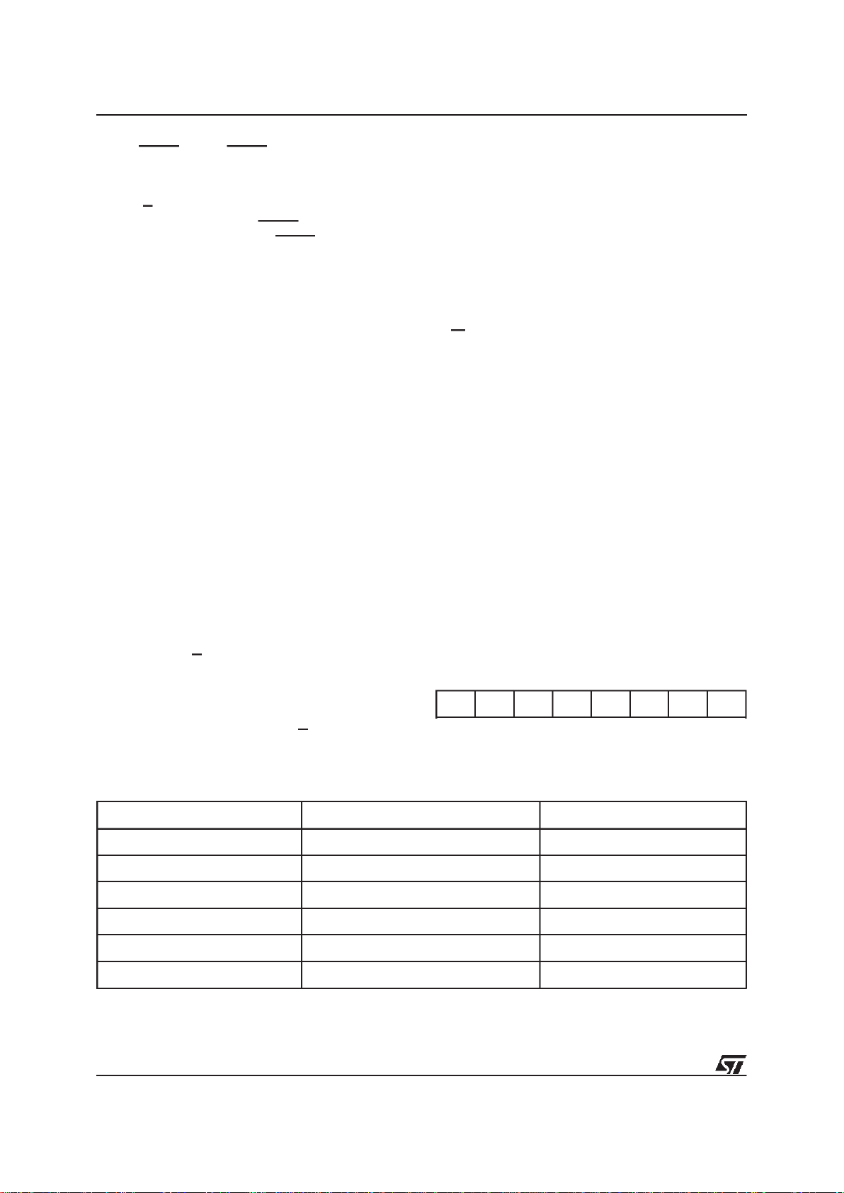
AI01272
HOLD
S
W Control Logic
High
Voltage
Generator
I/O Shift Register
Address
Register
and Counter
Data
Register
16 Bytes
X Decoder
Y Decoder
Block
Protect
C
D
Q
Status
Figure5. Block Diagram
During a write to the memory operation to the
memory array, all bits BP1, BP0, WEL, WIP are
valid and can be read. Duringa writeto thestatus
register, only the bits WEL and WIP are valid and
can be read. The values of BP1 and BP0 read at
thattimecorrespondtothepreviouscontentsofthe
statusregister.
TheWrite-In-Process(WIP)read-onlybit indicates
whethertheMemoryis busywith a writeoperation.
Whenset to a ’1’a writeis in progress,when set to
a ’0’no write is in progress.
The Write Enable Latch (WEL) read-only bit indicatesthe statusofthe writeenablelatch.Whenset
toa ’1’the latchis set,when set to a ’0’the latch is
reset. The Block Protect (BP0 and BP1) bits indicate the extent of the protectionemployed. These
bitsare set by the userissuing the WRSR instruction. These bits are non-volatile.
5/18
ST95040, ST95020, ST95010
Page 6
WriteStatus Register (WRSR)
TheWRSR instructionallowsthe user toselectthe
size of protected memory. The user may read the
blocks but will be unable to write within the protected blocks. The blocks and respective WRSR
controlbits are shown in Table4.
When the WRSR instruction and the 8 bits of the
Status Register are latched-in, the internal write
cycleis then triggered by therising edge of S.
Thisrising edge of S must appearno laterthanthe
16th clock cycle of the WRSR instruction of the
StatusRegistercontent (it must not appeara 17th
clockpulse before the rising edge of S), otherwise
the internal writesequence is not performed.
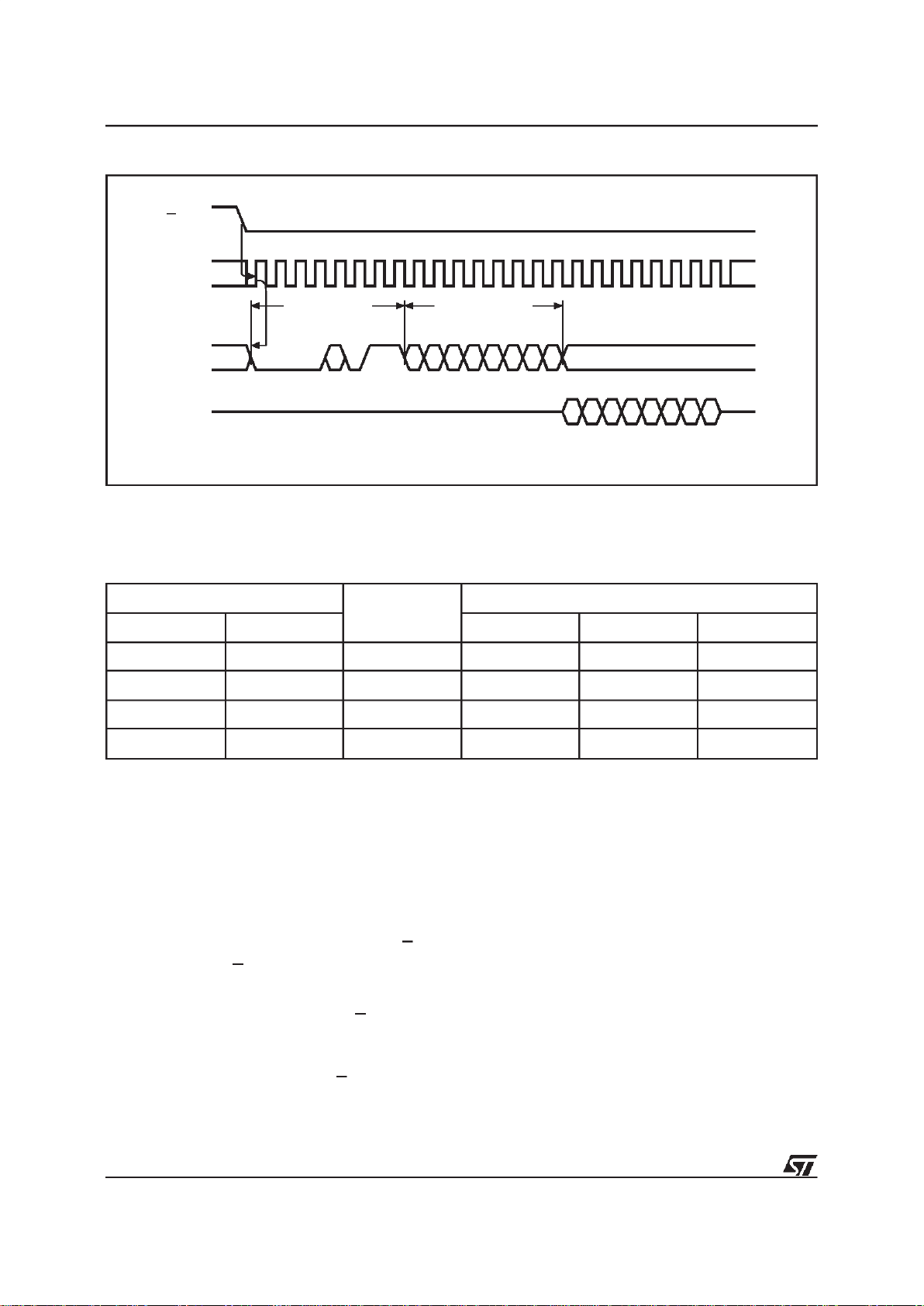
ReadOperation
Thechipis firstselectedby puttingS low.Theserial
one byte read instructionis followedby a one byte
address (A7-A0), each bit being latched-induring
the rising edge of the clock(C). Bit 3 (seeTable3)
of the read instruction contains address bit A8
(mostsignificantaddressbit). Thenthe datastored
inthememoryat theselectedaddressis shiftedout
on the Q output pin; each bit being shifted out
during the falling edge of the clock (C). The data
stored in the memory at the next addresscan be
read in sequence by continuing to provide clock
pulses. The byte address is automatically incrementedto the next higher addressafter each byte
of data is shiftedout. When the highestaddressis
reached,theaddresscounterrollsover to 0hallowing the read cycle to be continuedindefinitely.The
read operation is terminated by deselecting the
chip.Thechip canbe deselectedat anytimeduring
dataoutput. Any read attemptduring a write cycle
will be rejected and willdeselect the chip.
C
D
AI01440
S
Q
A7
21 3 4 5 6 7 8 9 10111213141516171819
A6 A5 A4 A3 A2 A1 A0A8
20 21 22 23
765432 0
1
HIGH IMPEDANCE
DATA OUT
INSTRUCTION BYTE ADDRESS
0
Figure 6. Read Operation Sequence
Status Register Bits
Protected Block
Array AddressProtected
BP1 BP0 ST95040 ST95020 ST95010
0 0 none none none none
0 1 Upper quarter 180h - 1FFh C0h - FFh 60h -7Fh
1 0 Upper half 100h - 1FFh 80h - FFh 40h - 7Fh
1 1 Whole memory 000h - 1FFh 00h - FFh 00h - 7Fh
Table4. WriteProtected Block Size
Notes: A8= A7 = 0 onST95010; A8 = 0 on ST95020; A8is only activeon ST95040.
6/18
ST95040, ST95020, ST95010
Page 7

C
D
AI01442
S
Q
A7
21 3 4 5 6 7 8 9 10 11 12 13 14 15 16 17 18 19
A6 A5 A4 A3 A2 A1 A0A8
20 21 22 23
HIGH IMPEDANCE
INSTRUCTION BYTE ADDRESS
0
765432 0
1
DATA BYTE
Figure8. Byte Write Operation Sequence
C
D
AI01441
S
Q
21 34567
HIGH IMPEDANCE
0
Figure7. WriteEnable Latch Sequence
Notes: A8= A7 = 0 onST95010; A8 = 0 on ST95020; A8is only activeon ST95040.
7/18
ST95040, ST95020, ST95010
Page 8

C
D
S
A7
21 3 4 5 6 7 8 9 10111213141516171819
A6 A5 A4 A3 A2 A1 A0A8
20 21 22 23
INSTRUCTION BYTE ADDRESS
0
765432 0
1
DATA BYTE 1
C
D
AI01443
S
7
2625 27 28 29 30 31 8+8N
63210
24
765432
1
DATA BYTE 16
9+8N
10+8N
11+8N
12+8N
13+8N
14+8N
15+8N
136
137
138
139
140
141
142
143
54
0
DATA BYTE N
76 321054
DATA BYTE 2
7
Figure9. PageWrite Operation Sequence
C
D
S
21 3 4 5 6 7 8 9 101112131415
INSTRUCTION
0
AI01444
Q
76543210
STATUS REG. OUT
HIGH IMPEDANCE
MSB
Figure10. RDSR:Read StatusRegisterSequence
Notes: A8= A7 = 0 onST95010; A8 = 0 on ST95020; A8is only activeon ST95040.
8/18
ST95040, ST95020, ST95010
Page 9

Byte Write Operation
Prior to any write attempt, the write enable latch
mustbe set by issuingthe WREN instruction.First
thedevice is selected(S = low)and aserialWREN
instructionbyte is issued. Then the product is deselectedby takingS high. Afterthe WRENinstruction byte is sent, the Memory will set the write
enable latch and then remain in standby until it is
deselected. Then the write state is entered by
selecting the chip, issuing two bytes of instruction
and address, and onebyte of data.
Chip Select (S) must remain low for the entire
duration of the operation. The product must be
deselectedjustaftertheeighthbitof data hasbeen
latchedin. If not,the writeprocess iscancelled.As
soon as the product is deselected, the self-timed
writecycleisinitiated.Whilethewrite isin progress,
thestatusregister maybe readto checkBP1,BP0,
WEL and WIP. WIP is high during the self-timed
writecycle. When the cycle is completed,the write
enablelatch is reset.
Page Write Operation
A maximum of 16 bytes of data may be written
during one non-volatile write cycle. All 16 bytes
must reside on the same page. The page write
mode is the same as the byte write mode except
thatinsteadof deselectingthe device after the first
byteofdata,upto15additionalbytescanbeshifted
in prior to deselecting the chip. A page address
beginswith addressxxxx 0000 and endswith xxxx
1111.Ifthe addresscounterreaches xxxx1111and
theclock continues,thecounter will roll overto the
firstaddressof the page (xxxx0000)and overwrite
any previously written data. The programmingcyclewill only startif the S transitionoccurs just after
the eighth bit of data of a word is received.
POWERON STATE
After a Power up the Memory is in the following
state:
– The device is in thelow power standbystate.
– The chip is deselected.
– The chip is not in holdcondition.
– The write enable latch is reset.
– BP1 and BP0 are unchanged (non-volatile
bits).
C
D
AI01445
S
Q
21 3 4 5 6 7 8 9 101112131415
HIGH IMPEDANCE
INSTRUCTION STATUS REG.
0
Figure11. WRSR: Write Status Register Sequence
9/18
ST95040, ST95020, ST95010
Page 10

DATAPROTECTIONAND PROTOCOLSAFETY
– All inputsare protectedagainstnoise, see Table
6.
– Non valid S and HOLD transitionsare not taken
into account.
– S must come high at the proper clock count in
order to start a non-volatilewrite cycle (in the
memory array or in the status register), that is
theChipSelectSmustriseduringtheclockpulse
followingthe introduction of a multiple of 8 bits.
– Access to the memory array during non-volatile
programmingcycleis ignored;however,the programmingcycle continues.
– Afteranyof theoperationsWREN,WRDI,RDSR
is completed, the chip enters a wait state and
waits for a deselect.
– The write enable latch is reset upon power-up.
– The writeenablelatchis resetwhenW isbrought
low.
INITIALDELIVERYSTATE
Thedevice is delivered with the memoryarray in a
fully erased state (all data set at all ”1’s” or FFh).
Theblock protect bits are initializedto00.
AI01446
MASTER
ST95xxx
D
Q
C
CQD
S
ST95xxx
CQD
S
ST95xxx
CQD
SCS3 CS2 CS1
Figure12. EEPROMand SPI Bus
10/18
ST95040, ST95020, ST95010
Page 11

AI00825
0.8V
CC
0.2V
CC
0.7V
CC
0.3V
CC
Figure13. AC Testing InputOutput Wavef.
Input Rise and FallTimes
≤
50ns
Input Pulse Voltages 0.2V
CC
to 0.8V
CC
Input and Output Timing
Reference Voltages
0.3V
CC
to 0.7V
CC
Output Load CL= 100pF
Note thatOutput Hi-Z is defined as the point where data is no
longer driven.
Table5. AC MeasurementConditions
Symbol Parameter Min Max Unit
C
IN
Input Capacitance (D) 8 pF
C
IN
Input Capacitance (other pins) 6 pF
t
LPF
Input Signal PulseWidth Filtered Out 10 ns
Note: 1. Sampled only,not 100% tested.
Table6. InputParameters
(1)
(TA=25°C, f = 2 MHz )
Symbol Parameter TestCondition Min Max Unit
I
LI
Input Leakage Current ±2 µA
I
LO
Output Leakage Current
±
2
µ
A
I
CC
Supply Current
C = 0.1 VCC/0.9 VCC,
@ 2 MHz, Q = Open
2mA
C = 0.1 V
CC
/0.9 VCC,
@ 2 MHz, Q = Open, Note 2
2mA
Supply Current (W series)
C = 0.1 V
CC
/0.9 VCC,
@ 1 MHz, V
CC
= 2.5V,
Q = Open
1.5 mA
I
CC1
Standby Current
S=V
CC,VIN=VSS
or V
CC
50 µA
S=V
CC,VIN=VSS
or VCC,
Note 2
50 µA
Standby Current (W series)
S=V
CC,VIN=VSS
or VCC,
V
CC
= 2.5V
25 µA
V
IL
Input Low Voltage – 0.3 0.3 V
CC
V
V
IH
Input High Voltage 0.7 V
CC
VCC+1 V
V
OL
(1)
Output Low Voltage
I
OL
= 2mA 0.4 V
I
OL
= 2mA,Note 2 0.4 V
Output Low Voltage(W series) I
OL
= 1.5mA, VCC= 2.5V 0.4 V
V
OH
(1)
Output High Voltage
I
OH
= –2mA VCC–0.6 V
I
OH
= –2mA, Note 2 VCC–0.6 V
Output High Voltage (W series) I
OH
= –0.4mA, VCC= 2.5V VCC–0.3 V
Notes: 1. The devicemeets output requirements for both TTL and CMOS standards.
2. Test performed at –40 to 125°C temperature range, grade 3.
Table7. DC Characteristics
(T
A
=0 to 70°C, –40 to 85°C or–40 to 125°C; VCC= 4.5V to 5.5V or 2.5Vto 5.5V)
11/18
ST95040, ST95020, ST95010
Page 12

Symbol Alt Parameter
ST95040 / 020 / 010
Unit
V
CC
= 4.5V to 5.5V,
T
A
= 0 to 70°C,
T
A
= –40 to 85°C
V
CC
= 4.5V to 5.5V,
T
A
= –40 to 125°C
V
CC
= 2.5V to 5.5V,
T
A
= 0 to 70°C,
T
A
= –40 to 85°C
Min Max Min Max Min Max
f
C
f
C
Clock Frequency D.C. 2 D.C. 2 D.C. 1 MHz
t
SLCH
t
CSS
S Active Setup Time 100 100 200 ns
t
CHSL
S Not Active Hold
Time
100 100 200 ns
t
CH
(1)
t
CLH
Clock High Time 190 200 400 ns
t
CL
(1)
t
CLL
Clock Low Time 200 200 400 ns
t
CLCH
t
RC
Clock Rise Time 1 1 1
µ
s
t
CHCL
t
FC
Clock Fall Time 1 1 1 µs
t
DVCH
t
DSU
Data In SetupTime 50 50 100 ns
t
CHDX
t
DH
Data In HoldTime 50 50 100 ns
t
DLDH
t
RI
Data In RiseTime 1 1 1
µ
s
t
DHDL
t
FI
Data In FallTime 1 1 1
µ
s
t
HHCH
t
HSU
HOLDSetup Time 100 100 200 ns
t
HLCH
Clock Low Hold Time 90 90 200 ns
t
CLHL
t
HH
HOLDHold Time 80 80 200 ns
t
CLHH
Clock Low Set-up
Time
100 100 200 ns
t
CHSH
S Active Hold Time 200 200 200 ns
t
SHCH
S Not Active Setup
Time
100 100 200 ns
t
SHSL
t
CSH
S Deselect Time 200 200 200 ns
t
SHQZ
t
DIS
Output Disable Time 150 150 200 ns
t
CLQV
t
V
Clock Low to Output
Valid
240 300 400 ns
t
CLQX
t
HO
Output Hold Time 0 0 0 ns
t
QLQH
(2)
t
RO
Output Rise Time 100 100 200 ns
t
QHQL
(2)
t
FO
Output Fall Time 100 100 200 ns
t
HHQX
t
LZ
HOLDHigh to Output
Low-Z
100 100 200 ns
t
HLQZ
t
HZ
HOLDLow to Output
High-Z
130 130 200 ns
t
W
t
WP
Write Cycle Time 10 10 10 ms
Notes:
1. t
CH+tCL
≥
1/fc
2. Value guaranteed by characterization, not 100% tested in production.
Table8. AC Characteristics
12/18
ST95040, ST95020, ST95010
Page 13

C
D
AI01447
S
MSB IN
Q
tDVCH
HIGH IMPEDANCE
LSB IN
tSLCH
tCHDX
tDLDH
tDHDL
tCHCL
tCLCH
tSHCH
tSHSL
tCHSHtCHSL
Figure14. SerialInput Timing
C
Q
AI01448
S
D
HOLD
tCLHL
tHLCH
tHHCH
tCLHH
tHHQXtHLQZ
Figure 15. Hold Timing
13/18
ST95040, ST95020, ST95010
Page 14

C
Q
AI01449B
S
LSB OUT
D
ADDR.LSB IN
tSHQZ
tCH
tCL
tQLQH
tQHQL
tCLQX
tCLQV
Figure16. OutputTiming
14/18
ST95040, ST95020, ST95010
Page 15

ORDERING INFORMATION SCHEME
Notes: 1. DataIn is strobed on rising edge of the clock (C) and Data Out is synchronized from the falling edge of the clock.
2. Temperature range on request only,5V ± 10% only.
Devicesare shipped from the factorywith thememory content set at all”1’s” (FFh).
For a list of availableoptions (OperatingVoltage,Package, etc...) or for further information on any aspect
of this device, pleasecontact the STMicroelectronicsSales Office nearest to you.
Density
04 4K (512 x 8)
02 2K (256 x 8)
01 1K (128 x 8)
Data Strobe
0 Note 1
Operating Voltage
blank 4.5V to 5.5V
W 2.5V to 5.5V
Package
B PSDIP8
0.25 mm Frame
M SO8
150mils Width
Option
TR Tape & Reel
Packing
TemperatureRange
1 0 to 70°C
6 –40 to 85 °C
3
(2)
–40 to 125 °C
Example: ST95xx0 W M 6 TR
15/18
ST95040, ST95020, ST95010
Page 16

PSDIP-a
A2A1A
L
e1
D
E1 E
N
1
C
eA
eB
B1
B
Symb
mm inches
Typ Min Max Typ Min Max
A 3.90 5.90 0.154 0.232
A1 0.49 – 0.019 –
A2 3.30 5.30 0.130 0.209
B 0.36 0.56 0.014 0.022
B1 1.15 1.65 0.045 0.065
C 0.20 0.36 0.008 0.014
D 9.20 9.90 0.362 0.390
E 7.62 – – 0.300 – –
E1 6.00 6.70 0.236 0.264
e1 2.54 – – 0.100 – –
eA 7.80 – 0.307 –
eB 10.00 0.394
L 3.00 3.80 0.118 0.150
N8 8
CP 0.10 0.004
Drawing is not to scale
PSDIP8 - 8 pin Plastic Skinny DIP, 0.25mm lead frame
16/18
ST95040, ST95020, ST95010
Page 17

SO-a
E
N
CP
B
e
A
D
C
LA1 α
1
H
hx45°
Symb
mm inches
Typ Min Max Typ Min Max
A 1.35 1.75 0.053 0.069
A1 0.10 0.25 0.004 0.010
B 0.33 0.51 0.013 0.020
C 0.19 0.25 0.007 0.010
D 4.80 5.00 0.189 0.197
E 3.80 4.00 0.150 0.157
e 1.27 – – 0.050 – –
H 5.80 6.20 0.228 0.244
h 0.25 0.50 0.010 0.020
L 0.40 0.90 0.016 0.035
α
0
°
8
°
0
°
8
°
N8 8
CP 0.10 0.004
Drawing is not to scale
SO8 - 8 lead Plastic Small Outline, 150 mils body width
17/18
ST95040, ST95020, ST95010
Page 18

Information furnished is believed to be accurate and reliable. However, STMicroelectronics assumes no responsibility for the consequences
of useof such informationnor for any infringementof patents or other rightsof third parties whichmay result from its use. No licenseis granted
by implication or otherwise under any patent or patent rights of STMicroelectronics.Specificationsmentioned in this publication are subject to
change without notice. This publication supersedes and replaces all information previously supplied. STMicroelectronics products are not
authorized for use as critical components in life support devices or systems without express written approval of STMicroelectronics.
The ST logois a registered trademark of STMicroelectronics
1998STMicroelectronics - All Rights Reserved
STMicroelectronics GROUP OF COMPANIES
Australia - Brazil - Canada- China - France- Germany - Italy - Japan - Korea - Malaysia - Malta - Morocco - The Netherlands -
Singapore - Spain - Sweden - Switzerland- Taiwan- Thailand - United Kingdom - U.S.A.
18/18
ST95040, ST95020, ST95010
 Loading...