

Page 1

General features
■ Half duplex frequency shift keying (FSK)
transceiver
■ Integrated power line driver with programmable
voltage and current control
■ Programmable interface:
– Synchronous
– Asynchronous
■ Single supply voltage (from 7.5 up to 12.5V)
■ Very low power consumption (Iq = 5mA)
■ Integrated 5V voltage regulator (up to 50mA)
with short circuit protection
■ Integrated 3.3V voltage regulator (up to 50mA)
with short circuit protection
■ 3.3V or 5V digital supply
■ 8 programmable transmission frequencies
■ Programmable baud rate up to 4800BPS
■ Receiving sensitivity up to 250µVrms
■ Suitable to application in accordance with EN
50065 CENELEC specifications
■ Carrier or preamble detection
■ Band in use detection
■ Programmable 24 or 48 bit register with
security checksum
■ Mains zero crossing detection and
synchronization
■ Watchdog timer
■ Output voltage freeze
■ 8 or 16 bit header recognition
■ UART/SPI host interface
■ ST7537 compatible
ST7538Q
FSK power line transceiver
TQFP44 Slug Down
Description
The ST7538Q is a Half Duplex
synchronous/asynchronous FSK Modem
designed for power line communication network
applications. It operates from a single supply
voltage and integrates a line driver and two linear
regulators for 5V and 3.3V. The device operation
is controlled by means of an internal register,
programmable through the synchronous serial
interface. Additional functions as watchdog, clock
output, output voltage and current control,
preamble detection, time-out, band in use are
included. Realized in Multipower BCD5
technology that allows to integrate DMOS, Bipolar
and CMOS structures in the same chip.
Order codes
Part number Package Packaging
ST7538Q TQFP44 Slug Down Tube
ST7538QTR TQFP44 Slug Down Tape and reel
July 2006 Rev 1 1/44
www.st.com
44
Page 2

Contents ST7538Q
Contents
1 Block diagram . . . . . . . . . . . . . . . . . . . . . . . . . . . . . . . . . . . . . . . . . . . . . . 4
2 Pin settings . . . . . . . . . . . . . . . . . . . . . . . . . . . . . . . . . . . . . . . . . . . . . . . . 5
2.1 Pin connection . . . . . . . . . . . . . . . . . . . . . . . . . . . . . . . . . . . . . . . . . . . . . . 5
2.2 Pin description . . . . . . . . . . . . . . . . . . . . . . . . . . . . . . . . . . . . . . . . . . . . . . 6
3 Electrical data . . . . . . . . . . . . . . . . . . . . . . . . . . . . . . . . . . . . . . . . . . . . . . 8
3.1 Maximum ratings . . . . . . . . . . . . . . . . . . . . . . . . . . . . . . . . . . . . . . . . . . . . 8
3.2 Thermal data . . . . . . . . . . . . . . . . . . . . . . . . . . . . . . . . . . . . . . . . . . . . . . . 9
4 Electrical characteristics . . . . . . . . . . . . . . . . . . . . . . . . . . . . . . . . . . . . . 9
5 Functional description . . . . . . . . . . . . . . . . . . . . . . . . . . . . . . . . . . . . . . 15
5.1 Carrier frequencies . . . . . . . . . . . . . . . . . . . . . . . . . . . . . . . . . . . . . . . . . . 15
5.2 Baud rates . . . . . . . . . . . . . . . . . . . . . . . . . . . . . . . . . . . . . . . . . . . . . . . . 15
5.3 Mark and space frequencies . . . . . . . . . . . . . . . . . . . . . . . . . . . . . . . . . . 16
5.4 ST7538Q mains access . . . . . . . . . . . . . . . . . . . . . . . . . . . . . . . . . . . . . . 17
5.5 Host processor interface . . . . . . . . . . . . . . . . . . . . . . . . . . . . . . . . . . . . . 18
5.5.1 Communication between host and ST7538Q . . . . . . . . . . . . . . . . . . . . 20
5.6 Control register access . . . . . . . . . . . . . . . . . . . . . . . . . . . . . . . . . . . . . . . 21
5.7 Receiving mode . . . . . . . . . . . . . . . . . . . . . . . . . . . . . . . . . . . . . . . . . . . . 23
5.7.1 High sensitivity mode . . . . . . . . . . . . . . . . . . . . . . . . . . . . . . . . . . . . . . . 23
5.7.2 Synchronization recovery system (PLL) . . . . . . . . . . . . . . . . . . . . . . . . 23
5.7.3 Carrier/preamble detection . . . . . . . . . . . . . . . . . . . . . . . . . . . . . . . . . . 24
5.7.4 Header recognition . . . . . . . . . . . . . . . . . . . . . . . . . . . . . . . . . . . . . . . . 24
5.8 Transmission mode . . . . . . . . . . . . . . . . . . . . . . . . . . . . . . . . . . . . . . . . . 26
5.8.1 Automatic Level Control (ALC) . . . . . . . . . . . . . . . . . . . . . . . . . . . . . . . . 27
5.9 Crystal oscillator . . . . . . . . . . . . . . . . . . . . . . . . . . . . . . . . . . . . . . . . . . . . 30
5.10 Control register . . . . . . . . . . . . . . . . . . . . . . . . . . . . . . . . . . . . . . . . . . . . . 31
5.11 Detection method and Rx Sensitivity in UART mode . . . . . . . . . . . . . . . . 35
2/44
Page 3

ST7538Q Contents
6 Auxiliary analog and digital functions . . . . . . . . . . . . . . . . . . . . . . . . . 36
6.1 Band in use . . . . . . . . . . . . . . . . . . . . . . . . . . . . . . . . . . . . . . . . . . . . . . . 36
6.2 Time out . . . . . . . . . . . . . . . . . . . . . . . . . . . . . . . . . . . . . . . . . . . . . . . . . . 36
6.3 Reset & watchdog . . . . . . . . . . . . . . . . . . . . . . . . . . . . . . . . . . . . . . . . . . 36
6.4 Zero crossing detection . . . . . . . . . . . . . . . . . . . . . . . . . . . . . . . . . . . . . . 37
6.5 Output clock . . . . . . . . . . . . . . . . . . . . . . . . . . . . . . . . . . . . . . . . . . . . . . . 38
6.6 Output voltage level freeze . . . . . . . . . . . . . . . . . . . . . . . . . . . . . . . . . . . . 38
6.7 Extended control register . . . . . . . . . . . . . . . . . . . . . . . . . . . . . . . . . . . . . 38
6.8 Reg OK . . . . . . . . . . . . . . . . . . . . . . . . . . . . . . . . . . . . . . . . . . . . . . . . . . 38
6.9 Under voltage lock out . . . . . . . . . . . . . . . . . . . . . . . . . . . . . . . . . . . . . . . 38
6.10 Thermal shutdown . . . . . . . . . . . . . . . . . . . . . . . . . . . . . . . . . . . . . . . . . . 38
6.11 5V and 3.3V voltage regulators and power good function . . . . . . . . . . . . 39
6.12 Power-up procedure . . . . . . . . . . . . . . . . . . . . . . . . . . . . . . . . . . . . . . . . . 40
7 Package mechanical data . . . . . . . . . . . . . . . . . . . . . . . . . . . . . . . . . . . . 42
8 Revision history . . . . . . . . . . . . . . . . . . . . . . . . . . . . . . . . . . . . . . . . . . . 43
3/44
Page 4

Block diagram ST7538Q
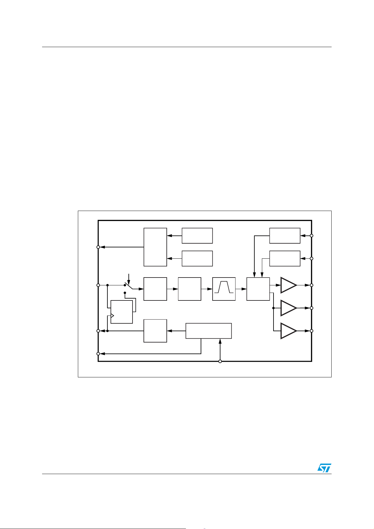
1 Block diagram
Figure 1. Block diagram
CD/PD
RxD
CLR/T
UART/SPI
REG/DATA
RxTx
TxD
REGOK
SERIAL
INTERFACE
XOut WD
XIn
TEST2TEST1AVdd AVss BU
CARRIER
DETECTION
PLL
TIME BASE
TOUT RSTO MCLK ZCout ZCin C_OUT CMINUS CPLUS
DIGITAL
FILTER
CONTROL
REGISTER
FSK
MODULATOR
ZCOSC
FSK
DEMOD
DAC
TEST
OP-AMP
IF
FILTER
TX
FILTER
+
-
BU
FILTER
ALC
VREG
DVdd DVss
AGC
AMPL
CURRENT
CONTROL
VOLTAGE
CONTROL
PLI
RxFo
RAI
FILTER
CL
Vsense
ATO
ATOP1
ATOP2
PAVcc
Vdc
PG
D03IN1407A
4/44
Page 5

ST7538Q Pin settings
2 Pin settings
2.1 Pin connection
Figure 2. Pin Connection (Top view)
N.C.
TEST1
REG_OK
C_MINUS
C_PLUS
N.C.
C_OUT
GND
PG
REG_DATA
N.C.
44 43 42 413940 38 37 36 35 34
CD_PD
DVSS
RXD
RxTx
TXD
GND
TOUT
CLR/T
BU
DVDD
MCLK
1
2
3
4
5
6
7
8
9
10
12 13 14 15 16
171118 19 20 21 22
33
32
31
30
29
28
27
26
25
24
23
VDC
RAI
RXFO
TEST2
VSENSE
AVDD
XIN
XOUT
SGND
ATO
CL
RSTO
WD
UART/SPI
ZCIN
ZCOUT
N.C.
DVSS
ATOP1
PAVSS
ATOP2
PAVCC
D01IN1312
5/44
Page 6

Pin settings ST7538Q
2.2 Pin description
Table 1. Pin description
Pin N° Name Type Description
1 CD_PD Digital/Output Carrier, Preamble or Frame Header Detect Output.
"1" No Carrier, Preamble or Frame Header Detected
"0" Carrier, Preamble or Frame Header Detected
2 DVss Supply Digital Ground
3 RxD Digital/Output RX Data Output.
4 RxTx Digital/Input
with internal pull-up
Rx or Tx mode selection input.
"1" - RX Session
"0" - TX Session
5 TxD Digital/Input
TX Data Input.
with internal pull-down
6 GND Supply Substrate Ground (same function as PIN 41)
7 TOUT Digital/Output TX Time Out Event Detection
"1" - Time Out Event Occurred
"0" - No Time-out Event Occurred
8 CLR/T Digital/Output Synchronous Mains Access Clock or
Control Register Access Clock
9 BU Digital/Output Band in use Output.
"1" Signal within the Programmed Band
"0" No Signal within the Programmed Band
10 DVdd Supply Digital Supply Voltage or 3.3V Voltage Regulator Output
11 MCLK Digital/Output Master Clock Output
12 RSTO Digital/Output Power On or Watchdog Reset Output
13 UART/SPI Digital/Input
with internal pull-down
Interface type:
“0” - Serial Peripheral Interface
“1” - UART Interface
14 WD Digital/Input
with internal pull-up
Watchdog input. The Internal Watchdog Counter is cleared on the
falling edges.
15 ZCOUT Digital/Output Zero Crossing Detection Output
(1)
16
ZCIN
Analog/Input Zero Crossing AC Input.
17 NC Floating Must be connected to DVss.
18 DVss Supply Digital Ground
19 ATOP1 Power/Output Power Line Driver Output
20 PAVss Supply Power Analog Ground
21 ATOP2 Power/Output Power Line Driver Output
22 PAV
23
CL
Supply Power Supply Voltage
CC
(2)
Analog/Input Current Limiting Feedback.
A resistor between CL and AVss sets the PLI Current Limiting Value
An integrated 80pF filtering input capacitance is present on this pin
24 ATO Analog/Output Small Signal Analog Transmit Output
6/44
Page 7

ST7538Q Pin settings
Table 1. Pin description (continued)
Pin N° Name Type Description
25 SGND Supply Analog Signal Ground
26 XOUT Analog Output Crystal Output
27 XIN Analog Input Crystal Oscillator Input - External Clock Input
28 AVdd Supply Analog Power supply.
(3)
29
Vsense
30 TEST2 Analog/Input Test Input must be connected SGND
31 RxFO Analog/Output Receiving Filter Output
32 RAI Analog/Input Receiving Analog Input
33 VDC Power 5V Voltage Regulator Output
34 NC floating Must Be connected to DVss.
35 TEST1 Digital/Input
36 REGOK Digital/Output Security checksum logic output
37
C_MINUS
38
C_PLUS
Analog/Input Output Voltage Sensing input for the voltage control loop
Test input. Must Be connected to DVss.
with internal pull-down
"1" - Stored data Corrupted
"0" - Stored data OK
(4)
Analog/Input Op-amp Inverting Input.
(5)
Analog/Input Op-amp Not Inverting Input.
39 NC floating Must Be connected to DVss
40 C_OUT Analog/Output Op-amp Output
41 GND Supply Substrate Ground (same function as PIN 6)
42 PG Digital/Output Power Good logic Output
"1" - VDC is above 4.5V and DVdd is above 3.125V
"0" - VDC is below 4.25V or DVdd is below 2.875V
43 REG_DATA Digital/Input
with internal pull-down
Mains or Control Register Access Selector
"1" - Control Register Access
"0" - Mains Access
44 NC floating Must be connected to DVss.
1. If not used this pin must be connected to VDC
2. Cannot be left floating
3. Cannot be left floating
4. If not used this pin must be connected to VDC
5. If not used this pin must be tied low (SGND or PAVss or DVss)
7/44
Page 8

Electrical data ST7538Q
3 Electrical data
3.1 Maximum ratings
Table 2. Absolute maximum ratings
Symbol Parameter Value Unit
PAV
AV
DV
AVss/DVss Voltage between AVss and DVss
Power Supply Voltage -0.3 to +14 V
CC
Analog Supply Voltage -0.3 to +5.5 V
dd
Digital Supply Voltage -0.3 to +5.5 V
dd
-0.3 to +0.3 V
V
V
I
V
sense
XIN,
C_MINUS
,C_PLUS,
Digital input Voltage
I
Digital output Voltage
O
Digital Output Current -2 to +2 mA
O
,
Voltage Range at Vsense, XIN, C_MINUS,
C_PLUS, CL Inputs
CL
RAI,
ZCIN
Voltage Range at RAI, ZCIN Inputs
ATO,
RxFO,
C_OUT,
Voltage range at ATO, RxFO, C_OUT, XOUT
Outputs
XOUT
ATOP1,2 Voltage range at Powered ATO Output
ATO P
T
amb
T
CD_PD
Pin
Other
pins
1. This current is intended as not repetitive pulse current
Powered ATO Output Current
Operating ambient Temperature -40 to +85 °C
Storage Temperature -50 to 150 °C
stg
Maximum Withstanding Voltage Range
Test Condition: CDF-AEC-Q100-002- “Human Body
Model”
Acceptance Criteria: “Normal Performance”
(1)
- 0.3 to DVdd +0.3
DV
ss
DV
- 0.3 to DVdd +0.3
ss
- 0.3 to AVdd+0.3
AV
ss
- 0.3 to AVdd +0.3
-AV
dd
AVss - 0.3 to AVdd +0.3
- 0.3 to +PAVcc
AV
ss
+0.3
400 mArms
±1500 V
±2000 V
V
V
V
V
V
V
8/44
Page 9

ST7538Q Electrical characteristics
3.2 Thermal data
Table 3. Thermal data
Symbol Parameter
TQFP44
with slug
Unit
R
thJA1
R
thJA2
1. Mounted on Multilayer PCB with a dissipating surface on the bottom side of the PCB
2. It's the same condition of the point above, without any heatsinking surface on the board.
Maximum Thermal Resistance Junction-Ambient
Steady state
(1)
Maximum Thermal Resistance Junction-Ambient
Steady state
(2)
35 ° C/W
50 ° C/W
4 Electrical characteristics
Table 4. Electrical characteristics
(AVdd = DVdd = +5V, PAVcc =+9 V, PAVss, SGND = DVss = 0V, -40°C ≤ TA ≤ 85°C, TJ < 125 °C, fc = 86kHz,
other control register parameters as default value, unless otherwise specified)
Symbol Parameter Test condition Min Typ Max Unit
, DV
AV
dd
PAVdd - DV
- AV
PAV
CC
PAV
+ DI
AI
dd
Supply voltages 4.75 5 5.25 V
dd
PAVCC and DVdd Relation
during Power-Up
dd
Sequence
DVdd < 4.75V with 5V
Digital supply provided
externally
0.1 1.2 V
PAVCC and AVdd Relation
during Power-Up
dd
AVdd < 4.75V
0.1 1.2 V
Sequence
Power Supply Voltage 7.5 12.5 V
cc
Max allowed slope during
Power-Up
Input Supply Current
dd
Transmission &
Receiving mode
57mA
100 V/ms
I PAV
CC
UVLO
UVLO
HYS
Digital I/O
R
down
R
up
TX mode (no load) 30 50 mArms
Powered Analog Supply
Current
RX mode 500 1000 µA
Maximum total current 370 mArms
Input Under Voltage Lock
Out
3.7 3.9 4.1 V
Threshold on PAVcc
UVLO Hysteresis 340 mV
Pull Down Resistor 100 kΩ
Pull up Resistor 100 kΩ
9/44
Page 10

Electrical characteristics ST7538Q
Table 4. Electrical characteristics (continued)
(AVdd = DVdd = +5V, PAVcc =+9 V, PAVss, SGND = DVss = 0V, -40°C ≤ TA ≤ 85°C, TJ < 125 °C, fc = 86kHz,
other control register parameters as default value, unless otherwise specified)
Symbol Parameter Test condition Min Typ Max Unit
Digital I/O 5V digital supply
V
IH
V
IL
V
OH
V
OL
High Logic Level Input
Voltage
Low Logic Level input
Voltage
High Logic Level Output
Voltage
Low Logic Level Output
Voltage
IOH= -2mA
= 2mA
I
OL
2V
1.2 V
DVd d - 0.75 V
DVss + 0.3 V
Digital I/O 3.3V digital supply
V
IH
V
IL
V
OH
V
OL
High Logic Level Input
Voltage
Low Logic Level input
Voltage
High Logic Level Output
Voltage
Low Logic Level Output
Voltage
IOH= -2mA
= 2mA
I
OL
1.4 V
0.8 V
DVd d - 0.75 V
DVss + 0.4 V
Oscillator
XIN
XIN
SWING
OFFSET
XIN Input Voltage swing External Clock. Figure 19 5V
XIN Input Voltage offset External Clock. Figure 19 2.5 V
DC XTAL Clock Duty Cycle External Clock. Figure 19 40 60 %
Xtal
Crystal Oscillator
frequency
Fundamental 16 MHz
Tclock Oscillator Period (1/Xtal) 62.5 ns
Xtal
Xtal
ESR
External Oscillator Esr
Resistance
External Oscillator
CL
Stabilization Capacitance
40 Ω
16 pF
Transmitter
IATO
V
ATO
V
ATO D C
Output Transmitting
Current on ATO
= 1.75kΩ
Max Carrier Output AC
Voltage
R
CL
Vsense
(AC) = 0V
Output DC Voltage on ATO 1.7 2.1 2.5 V
10/44
1mArms
1.75 2.3 3.5
V
PP
Page 11

ST7538Q Electrical characteristics
Table 4. Electrical characteristics (continued)
(AVdd = DVdd = +5V, PAVcc =+9 V, PAVss, SGND = DVss = 0V, -40°C ≤ TA ≤ 85°C, TJ < 125 °C, fc = 86kHz,
other control register parameters as default value, unless otherwise specified)
Symbol Parameter Test condition Min Typ Max Unit
HD2
HD3
IATOP
V
ATO P ( AC )
V
ATO P ( DC )
HD2
HD3
VATOP
ATO
ATO
ATO P
ATO P
Second Harmonic
Distortion on ATO
Third Harmonic Distortion
on ATO
Output Transmitting
Current in programmable
current limiting
Max Carrier Output AC
Voltage for each ATOP1
and ATOP2 pins
Output DC Voltage on
ATOP1 and ATOP2 pins
Second Harmonic
Distortion on each ATOP1
and ATOP2 pins
Third Harmonic Distortion
on each ATOP1 and
ATOP2 pins
Accuracy with Voltage
Control Loop Active
V
= 2V
ATO
Rcl = 1.85kΩ; R
PP
LOAD
1Ω (as in Figure 14)
R
= 1.t5kΩ
CL
(AC) = 0V
Vsense
ATO P
= 4V
VATOP AC()
----------------------------- ------- 7.5V+≥
2
,
PP
PAVcc
V
PAVCC = 10V
No Load
V
ATO P
= 4V
PP
,
PAVCC = 10V
=50Ω (Differential)
R
LOAD
Carrier Frequency:
132.5KHz
V
ATO P
= 4V
PP
,
PAVCC = 10V
No Load.
V
ATO P
= 4V
PP
,
PAVCC = 10V
=50Ω (Differential)
R
LOAD
Carrier Frequency:
132.5KHz
= 1.75Ω;
R
CL
(AC) = 0V
Vsense
=
-55 -42
-52 -49
dB
dB
c
c
250 310 370 mArms
3.5 4.6 6
V
pp
3.5 4.2 5 V
-55 -42
-65 -53
-56 -49
-65 -52
dB
dB
dB
dB
c
c
c
c
-1 +1 GST
GST
ALC Gain Step Control
loop gain step
0.6 1 1.4 dB
DRNG ALC Dynamic Range 30 dB
Voltage control loop
Vsense
Vsense
V
SENSE(DC)
V
SENSE
reference threshold on
TH
V
pin
sense
Hysteresis on Voltage loop
HYS
reference threshold
Output DC Voltage on
VSENSE
Figure 14 160 180 200
Figure 14 ±18 mV
1.865 V
VSENSE Input Impedance 36 kΩ
11/44
mV
PK
Page 12
Electrical characteristics ST7538Q
Table 4. Electrical characteristics (continued)
(AVdd = DVdd = +5V, PAVcc =+9 V, PAVss, SGND = DVss = 0V, -40°C ≤ TA ≤ 85°C, TJ < 125 °C, fc = 86kHz,
other control register parameters as default value, unless otherwise specified)
Symbol Parameter Test condition Min Typ Max Unit
C
CL
CCL
CCL
HYST
T
RxTx
TA LC
T
ST
Receiver
TH
Input capacitance on CL
pin
Current control loop
reference threshold on C
L
pin
Hysteresis on Current loop
reference threshold
Carrier Activation Time
Carrier Stabilization Time
From STEP 16 to zero or
From step 16 to step 31,
Tstep
80 pF
Figure 14 1.80 1.90 2.00 V
Figure 14 210 250 290 mV
Figure 17 - 600 Baud
Xtal=16MHz
Figure 17- 1200 Baud
Xtal=16MHz
Figure 17- 2400 Baud
Xtal=16MHz
Figure 17- 4800 Baud
Xtal=16MHz
Figure 17
Xtal =16MHz
Figure 17
Xtal =16MHz
0.01 1.6 ms
0.01 800 µs
0.01 400 µs
0.01 200 µs
3.2 ms
200 µs
Input Sensitivity (Normal
V
IN
Mode)
Input Sensitivity (High
Sens.)
V
IN
R
IN
Maximum Input Signal 2
Input Impedance 80 100 140 kΩ
Carrier detection sensitivity
(Normal Mode)
V
CD
V
BU
Carrier detection sensitivity
(High Sensitivity Mode)
Carrier detection sensitivity
(TxD line forced to “1”)
Band in Use Detection
Level
UART/SPI pin
forced to “1”
0.5 2
250
0.5 2
250
V
BU
77 85
mV
rms
µV
rms
V
rms
mV
rms
µV
rms
dB/
µVrms
dB/
µVrms
12/44
Page 13

ST7538Q Electrical characteristics
Table 4. Electrical characteristics (continued)
(AVdd = DVdd = +5V, PAVcc =+9 V, PAVss, SGND = DVss = 0V, -40°C ≤ TA ≤ 85°C, TJ < 125 °C, fc = 86kHz,
other control register parameters as default value, unless otherwise specified)
Symbol Parameter Test condition Min Typ Max Unit
5V voltage regulator
VDC
Linear regulator output
voltage
Power Good Output
PG
VDC
Voltage Threshold on VDC
pin
PG
VDC(HYS
PG on VDC pin Hysteresis 250 mV
)
3.3V voltage regulator
DVdd
Linear Regulator Output
Voltage
Power Good Output
PG
DVd d
Voltage Threshold on DVdd
pin
PG
DVdd
PG on DVdd pin Hysteresis 250 mV
HYS
(
)
Other functions
T
T
T
T
T
T
T
T
RSTO
WD
WM
WO
OUT
OFF
OFFD
CD
Reset Time
Watch-dog Pulse Width See Figure 21 3.5 ms
Watch-dog Pulse Period See Figure 21
Watch-dog Time Out See Figure 21 1.5 s
TX TIME OUT
Time Out OFF Time See Figure 20 125 ms
RxTx 0->1 vs. TOUT Delay See Figure 20 20 µs
Carrier Detection Time
selectable by register
0 < Io < 50mA
7.5V < PAVcc < 12.5V
0 < Io < 50mA
7.5V < PAVcc < 12.5V
See Figure 21;
Xtal = 16MHz
Control Register Bit 7
and Bit 8
See Figure 20
Control Register
bit 9 and bit10
Figure 11
-5% 5.05 +5% V
4.3 4.5 4.7 V
-5% 3.3 +5% V
3.125 V
50 ms
T
+
WD
3.5
1490 ms
1
3
500
1
3
5
s
µs
ms
ms
ms
T
M
B
DCD
CLK
AUD
CD_PD Propagation Delay Figure 11 300 500 µs
fclock
fclock/2
fclock/4
off
600
1200
2400
4800
MHz
Baud
Master Clock Output
Selectable by register
Baud rate
Control Register
bit 15 and bit 16
see Ta b le 1 1
Control Register
bit 3 and bit 4
see Ta b le 1 1
13/44
Page 14
Electrical characteristics ST7538Q
Table 4. Electrical characteristics (continued)
(AVdd = DVdd = +5V, PAVcc =+9 V, PAVss, SGND = DVss = 0V, -40°C ≤ TA ≤ 85°C, TJ < 125 °C, fc = 86kHz,
other control register parameters as default value, unless otherwise specified)
Symbol Parameter Test condition Min Typ Max Unit
T
B
Baud rate Bit Time
BAUD
)
(=1/
Control Register
bit 3 and bit 4
see Ta b le 1 1
1667
833
417
208
Zero crossing detection
Zero Crossing Detection
ZC
DEL
delay (delay between the
Figure 22 1 µs
ZCIN and ZCOUT signals)
ZC
ZC
ZC
(OFFSET)
(LOW)
(HIGH)
Zero Crossing Detection
Low Threshold
Zero Crossing Detection
High Threshold
-45 -5 mV
5+45mV
Zero Crossing Offset -20 +20 mV
Operational amplifier
C
OUT(Sync)
C
OUT(Source)
C
IN(Offset)
Max Sync Current 15 28 45 mA
Max Source Current -30 -20 -10 mA
Input Terminals OFFSET -38 +38 mV
GBWP Gain Bandwidth Product 6 7 9 MHz
Serial interface
µs
Ts Setup Time see Figure 5, 6, 7, 8 & 9 5ns
T
T
T
T
T
T
CRP
H
CR
CC
DS
DH
Hold Time see Figure 5, 6, 7, 8 & 9 2ns
CLR/T vs. REG_DATA or
RxTx
see Figure 5, 6, 7, 8 & 9
CLR/T vs. CLR/T see Figure 5, 6, 7, 8 & 9
Setup Time see Figure 5, 6, 7, 8 & 9
Hold Time see Figure 5, 6, 7, 8 & 9
T
B
/4 TB/2
T
B
/4 TB/2
T
B
T
H
T
B
2*T
TB/2
/4
B
14/44
Page 15
ST7538Q Functional description
5 Functional description
5.1 Carrier frequencies
ST7538Q is a multi frequency device: eight programmable Carrier Frequencies are available
(see Ta bl e 5 ).
Only one Carrier could be used a time. The communication channel could be varied during
the normal working Mode to realize a multifrequency communication.
Selecting the desired frequency in the Control Register the Transmission and Reception
filters are accordingly tuned.
Table 5. ST7538Q Channels List
FCarrier F (KHz)
F0 60
F1 66
F2 72
F3 76
F4 82.05
F5 86
5.2 Baud rates
ST7538Q is a multi Baud rate device: four Baud Rate are available (See Table 6.).
Table 6. ST7538Q mark and space tones frequency distance vs baud rate and deviation
Baud Rate [Baud]
600 600
1200 600
2400
4800 2400
1. Frequency deviation.
2. Deviation = ∆F / (Baud Rate)
3. Deviation 0.5 Not Allowed
4. Default value
F6 110
(1)
F7
(1)
∆F
(Hz)
1200
(4)
1200
2400
4800
(4)
132.5
Deviation
(3)
1
0.5
1
0.5
1
0.5
1
(2)
15/44
Page 16
Functional description ST7538Q
5.3 Mark and space frequencies
Mark and space communication frequencies are defined by the following formula:
F ("0") = FCarrier + [
F ("1") = FCarrier - [
∆F]/2
∆F]/2
∆F is the Frequency Deviation.
With Deviation = “0.5” the difference in terms of frequency between the mark and space
tones is half the Baudrate value (∆F = 0.5*BAudrate). When the Deviation = “1” the
difference is the Baudrate itself (∆F = Baudrate). The minimal Frequency Deviation is
600Hz.
Table 7. ST7538Q synthesized frequencies
Carrier
Frequency
(KHz)
60 600 -- 82.05 600 --
Baud
Deviation
Rate
1 59733 60221 1 81706 82357
1200 0.5 59733 60221 1200 0.5 81706 82357
1 59408 60547 1 81380 82682
2400 0.5 59408 60547 2400 0.5 81380 82682
1 58757 61198 1 80892 83171
4800 0.5 58757 61198 4800 0.5 80892 83171
1 57617 62337 1 79590 84473
Exact
Frequency [Hz]
(Clock=16MHz)
“1” “0” “1” “0”
Carrier
Frequen
cy
(KHz)
Baud
Rate
Deviation
Exact
Frequency [Hz]
(Clock=16MHz)
66 600 -- 86 600 --
1 65755 66243 1 85775 86263
1200 0.5 65755 66243 1200 0.5 85775 86263
1 65430 66569 1 85449 86589
2400 0.5 65430 66569 2400 0.5 85449 86589
1 64779 67220 1 84798 87240
4800 0.5 64779 67220 4800 0.5 84798 87240
1 63639 68359 1 83659 88379
16/44
Page 17
ST7538Q Functional description
Table 7. ST7538Q synthesized frequencies
Carrier
Frequency
(KHz)
72 600 -- 110 600 --
76 600 -- 132.5 600 --
Baud
Deviation
Rate
1 71777 72266 1 109701 110352
1200 0.5 71777 72266 1200 0.5 109701 110352
1 71452 72591 1 109375 110677
2400 0.5 71452 72591 2400 0.5 109375 110677
1 70801 73242 1 108724 111165
4800 0.5 70801 73242 4800 0.5 108724 111165
1 69661 74382 1 107585 112467
1 75684 76335 1 132161 132813
1200 0.5 75684 76335 1200 0.5 132161 132813
1 75358 76660 1 131836 133138
2400 0.5 75358 76660 2400 0.5 131836 133138
1 74870 77148 1 131348 133626
Exact
Frequency [Hz]
(Clock=16MHz)
“1” “0” “1” “0”
Carrier
Frequen
cy
(KHz)
Baud
Rate
Deviation
Exact
Frequency [Hz]
(Clock=16MHz)
4800 0.5 74870 77148 4800 0.5 131348 133626
1 73568 78451 1 130046 134928
5.4 ST7538Q mains access
ST7538Q can access the Mains in two different ways:
● Synchronous access
● Asynchronous access
The choice between the two types of access can be performed by means of Control
Register bit 14 (see Ta b le 1 1) and affects the ST7538Q data flow in Transmission Mode as
in Reception Mode (for how to set the communication Mode, see Section 5.5 on page 18).
In Data Transmission Mode:
– Synchronous Mains access: on clock signal provided by ST7538Q (CLR/T line)
rising edge, data transmission line (TxD line) value is read and sent to the FSK
Modulator. ST7538Q manages the Transmission timing according to the
BaudRate Selected.
– Asynchronous Mains access: data transmission line (TxD line) value enters
directly to the FSK Modulator. The Host Controller manages the Transmission
timing (CLR/T line should be neglected).
17/44
Page 18
Functional description ST7538Q
In Data Reception Mode:
– Synchronous Mains access: on clock signal recovered by a PLL from ST7538Q
(CLR/T line) rising edge, value on FSK Demodulator is read and put to the data
reception line (RxD line). ST7538Q recovers the bit timing according to the
BaudRate Selected.
– Asynchronous Mains access: Value on FSK Demodulator is sent directly to the
data reception line (RxD line). The Host Controller recovers the communication
timing (CLR/T line should be neglected).
5.5 Host processor interface
ST7538Q exchanges data with the host processor through a serial interface.
The data transfer is managed by REG_DATA and RxTx Lines, while data are exchanged
using RxD, TxD and CLR/T lines.
Four are the ST7538Q working modes:
● Data Reception
● Data Transmission
● Control Register Read
● Control Register Write
REG_DATA and RxTx lines are level sensitive inputs.
Table 8. Data and control register access bits configuration
REG_DATA RxTx
Data Transmission 0 0
Data Reception 0 1
Control Register Read 1 1
Control Register Write 1 0
ST7538Q features two type of Host Communication Interfaces:
–SPI
–UART
The selection can be done through the UART/SPI pin. If UART/SPI pin is forced to “0” SPI
interface is selected while if UART/SPI pin is forced to “1” UART interface is selected
(a)
. The
type of interface affects the Data Reception by setting the idle state of RxD line. When
ST7538Q is in Receiving mode (REG_DATA=”0” and RxTx =“1”) and no data are available
on mains (or RxD is forced to an idle state, i.e. with a conditioned Detection Method), the
RxD line is forced to “0” when UART/SPI pin is forced to ”0” or to “1” when UART/SPI pin is
forced to ”1”.
a. UART Interface Mode modifies also Control Register Functions and provides one more level of Rx sensitivity
(see par. 5.11)
18/44
Page 19
ST7538Q Functional description
The UART interface allows to connect an UART compatible device instead SPI interface
allows to connect an SPI compatible device. The allowed combinations of Host
Interface/ST7538Q Mains Access are:
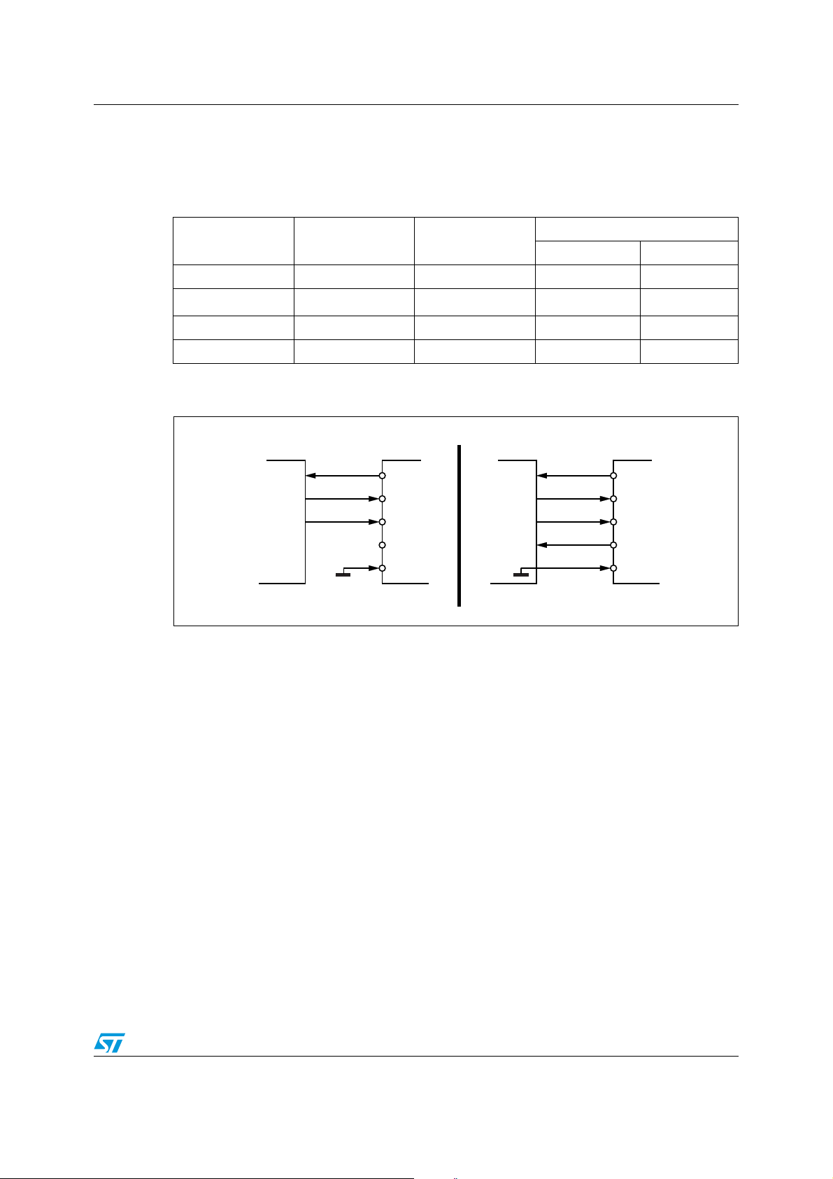
Table 9. Host Interface / ST7538Q mains access combinations
Host Device
interface type
UART/SPI pin
Communication
mode
UART “1” Transmission X
UART “1” Reception X
SPI “0” Transmission X
SPI “0” Reception X
1. Received Data more stable than in Asynchronous Mains Access
Asynchronous Synchronous
Mains access
(1)
X
Figure 3. Synchronous and asynchronous ST7538Q/Host controller interfaces
UART/Asynchronous
Data Interface
RxD
TxD
RxTx
CLR/T
REG_DATA
ST7538QHost Controller
SPI/Synchronous
Data Interface
D03IN1415
RxD
TxD
RxTx
CLR/T
REG_DATA
ST7538QHost Controller
ST7538Q allows to interface the Host Controller using a five line interface (RxD,TxD,RxTx,
CLR/T, & REG_DATA) in case of Synchronous mains access or using a 3 line interface
(RxD,TxD & RxTx) in Asynchronous mains access. Since Control Register is not accessible
in Asynchronous mode, in this case REG_DATA pin can be tied to GND.
19/44
Page 20
Functional description ST7538Q
5.5.1 Communication between host and ST7538Q
The Host can achieve the Mains access by selecting REG_DATA = ”0” and the choice
between Data Transmission or Data Reception is performed by selecting RxTx line
(if RxTx =“1” ST7538Q receives data from mains, if RxTx = ”0” ST7538Q transmits data over
the mains).
Communication between Host and ST7538Q is different in Asynchronous and Synchronous
mode:
● Asynchronous mode
In Asynchronous Mode, data are exchanged without any data Clock reference. The
host controller has to recover the clock reference in receiving Mode and control the Bit
time in transmission mode.
If RxTx line is set to “1” & REG_DATA = ”0” (Data Reception), ST7538Q enters in an
Idle State. After Tcc time the modem starts providing received data on RxD line.
If RxTx line is set to “0” & REG_DATA=”0” (Data Transmission), ST7538Q enters in an
Idle State and transmission circuitry is switched on. After Tcc time the modem starts
transmitting data present on TxD line.
● Synchronous mode
In Synchronous Mode ST7538Q is always the master of the communication and
provides the clock reference on CLR/T line.
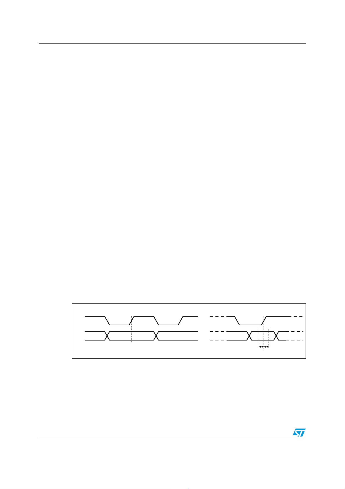
When ST7538Q is in receiving mode an internal PLL recovers the clock reference.
Data on RxD line are stable on CLR/T rising Edge.
When ST7538Q is in transmitting mode the clock reference is internally generated and
TxD line is sampled on CLR/T rising Edge.
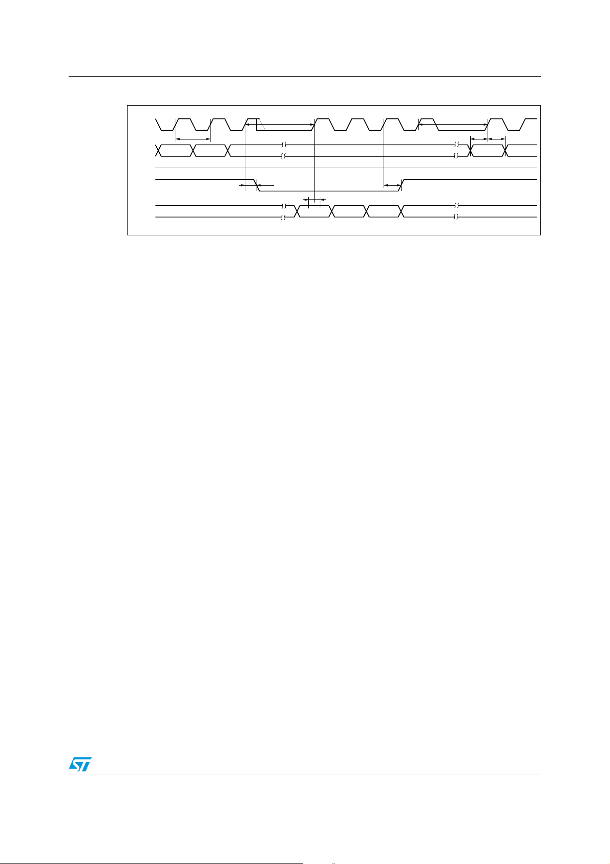
If RxTx line is set to “1” & REG_DATA=”0” (Data Reception), ST7538Q enters in an Idle
State and CLR/T line is forced Low. After Tcc time the modem starts providing received
data on RxD line.
If RxTx line is set to “0” & REG_DATA=”0” (Data Transmission), ST7538Q enters in an
Idle State and transmission circuitry is switched on. After Tcc time the modem starts
transmitting data present on TxD line (Figure 5) .
Figure 4. Receiving and transmitting data/recovered clock timing
Receiving Bit Synchronization
CLR/T
RxD
20/44
D03IN1416
CLR/T
TxD
Transmitting Bit Synchronization
TST
H
Page 21
ST7538Q Functional description
Figure 5. Data reception -> data transmission -> data reception
CLR_T
RxD
REG_DATA
RxTx
TxD
T
B
T
CR
5.6 Control register access
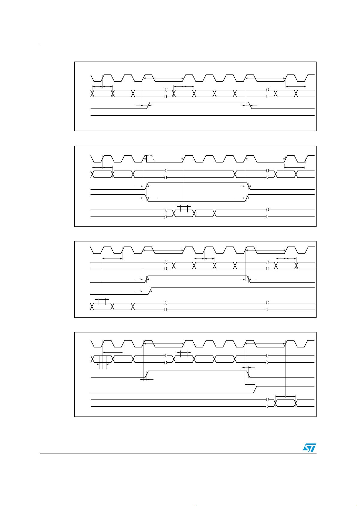
The communication with ST7538Q Control Register is always synchronous. The access is
achieved using the same lines of the Mains interface (RxD, TxD, RxTx and CLR/T) plus
REG_DATA Line.
With REG_DATA = 1 and RxTx = 0, the data present on TxD are loaded into the Control
Register MSB first. The ST7538Q samples the TxD line on CLR/T rising edges. The control
Register content is updated at the end of the register access section (REG_DATA falling
edge).
In Normal Control Register mode (Control Register bit 21=”0”, see Ta bl e 11 ) if more than 24
bits are transferred to ST7538Q only latest 24 bits are stored inside the Control Register. If
less than 24 bits are transferred to ST7538Q the Control Register writing is aborted (in this
case if at least 16 bits are provided REGOK line will be activated).
T
CC
TST
H
BIT23 BIT22
T
CC
T
T
DS
DH
T
CR
D03IN1402
In order to avoid undesired Control Register writings caused by REG_DATA line fluctuations
(for example because of surge or burst on mains), in Extended Control Register mode
(Control Register bit 21=”1” see Tab l e 1 1) exactly 24 or 48 bits must be transferred to
ST7538Q in order to properly write the Control Register, otherwise writing is aborted and if
at least 16 bits are provided REGOK line will be activated. If 24 bits are transferred, only the
first 24 Control Register bits (from 23 to 0) are written.
With REG_DATA = 1 and RxTx = 1, the content of the Control Register is sent on RxD port.
The Data on RxD are stable on CLR/T rising edges MSB First. In Normal Control Register
mode 24 bits are transferred from ST7538Q to the Host. In Extended Control Register mode
24 or 48 bits are transferred from ST7538Q to the Host depending on content of Control
Register bit 18 (with bit 18 = ”0” the first 24 bits are transferred, otherwise all 48 bits are
transferred, see Tab l e 1 1).
21/44
Page 22
Functional description ST7538Q
Figure 6. Data reception -> control register read -> data reception timing diagram
CLR_T
RXD
REG_DATA
RxTx
TDST
T
CC
DH
TDST
DH
BIT23 BIT22
T
CR
T
CC
T
B
T
CR
D03IN1404
Figure 7. Data reception -> control register write -> data reception timing diagram
CLR_T
RxD
REG_DATA
RxTx
TxD
T
CC
T
T
DH
DS
T
CR
T
CR
TST
H
T
CR
BIT23 BIT22
T
CC
T
B
T
CR
D03IN1403
Figure 8. Data transmission -> control reg. read data -> reception timing diagram
CLR_T
RxD
T
CC
T
B
TDST
DH
BIT23 BIT22
T
CC
TDST
DH
T
REG_DATA
RxTx
TST
H
CR
T
CR
TxD
Figure 9. Data transmission -> control reg. write -> data reception timing diagram
T
CLR_T
T
B
TxD
TST
REG_DATA
H
RxTx
RxD
22/44
CC
T
CR
TST
H
BIT23 BIT22
T
CR
D03IN1405
T
CC
T
CR
T
CR
T
T
DS
DH
D03IN1401
Page 23

ST7538Q Functional description
5.7 Receiving mode
The receive section is active when RxTx Pin = ”1” and REG_DATA = 0.
The input signal is read on RAI Pin using SGND as ground reference and then pre-filtered
by a Band pass Filter (62kHz max bandwidth at -3dB). The Pre-Filter can be inserted setting
one bit in the Control Register. The Input Stage features a wide dynamic range to receive
Signal with a Very Low Signal to Noise Ratio. The Amplitude of the applied waveform is
automatically adapted by an Automatic Gain Control block (AGC) and then filtered by a
Narrow Band Band-Pass Filter centered around the Selected Channel Frequency (14kHz
max at -3dB). The resulting signal is down-converted by a mixer using a sinewave generated
by the FSK Modulator. Finally an Intermediate Frequency Band Pass-Filter (IF Filter)
improves the Signal to Noise ration before sending the signal to the FSK demodulator. The
FSK demodulator then send the signal to the RX Logic for final digital filtering. Digital
filtering Removes Noise spikes far from the BAUD rate frequency and Reduces the Signal
Jitter. RxD Line is forced at logic level “0” or “1” (according the UART/SPI pin level) when
neither mark or space frequencies are detected on RAI Pin.
Mark and Space Frequency in Receiving Mode must be distant at least BaudRate/2 to have
a correct demodulation.
While ST7538Q is in Receiving Mode (RxTx pin = ”1”), the transmit circuitry, Power Line
Interface included, is turned off. This allows the device to achieve a very low current
consumption (5mA typ). In Receiving mode ATOP2 pin is internally connected to PAVSS.
5.7.1 High sensitivity mode
It is possible to increase the ST7538Q Receiving Sensitivity setting to ‘1’ the High Sensitivity
Bit of Control Register
when the ST7538Q sensitivity is the limiting factor.
(b)
. This function allows to increase the communication reliability
5.7.2 Synchronization recovery system (PLL)
ST7538Q embeds a Clock Recovery System to feature a Synchronous data exchange with
the Host Controller.
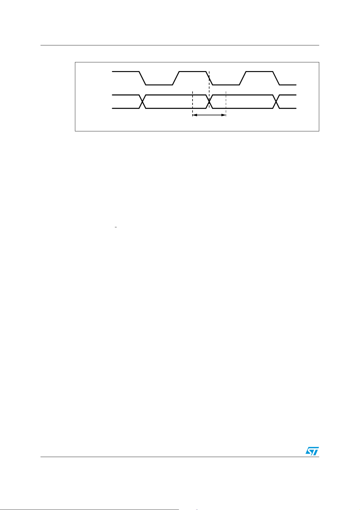
The clock recovery system is realized by means of a second order PLL. Data on the data
line (RxD) are stable on CLR/T line rising edge (CLR/T Falling edge synchronized to RxD
line transitions ± LOCK-IN Range).
The PLL Lock-in and Lock-out Range is ±π/2. When the PLL is in the unlock condition,
CLR/T and RxD lines are forced to a low logic level.
When PLL is in unlock condition it is sensitive to RxD Rising and Falling Edges. The
maximum number of transition required to reach the lock-in condition is 5. When in lock-in
condition the PLL is sensitive only to RxD rising Edges to reduce the CLR/T Jitter.
ST7538Q PLL is forced in the un-lock condition, when more than 32 equal symbols are
received.
Due to the fact that the PLL, in lock-in condition, is sensitive only to RxD rising edge,
sequences equal or longer than 15 equal symbols can put the PLL into the un-lock
condition.
b. A third level of Rx sensitivity can be selected in UART Interface Mode (see par. 5.11)
23/44
Page 24
Functional description ST7538Q
Figure 10. ST7538Q PLL lock-in range
CLR/T
RxD
D03IN1417
LOCK-IN RANGE
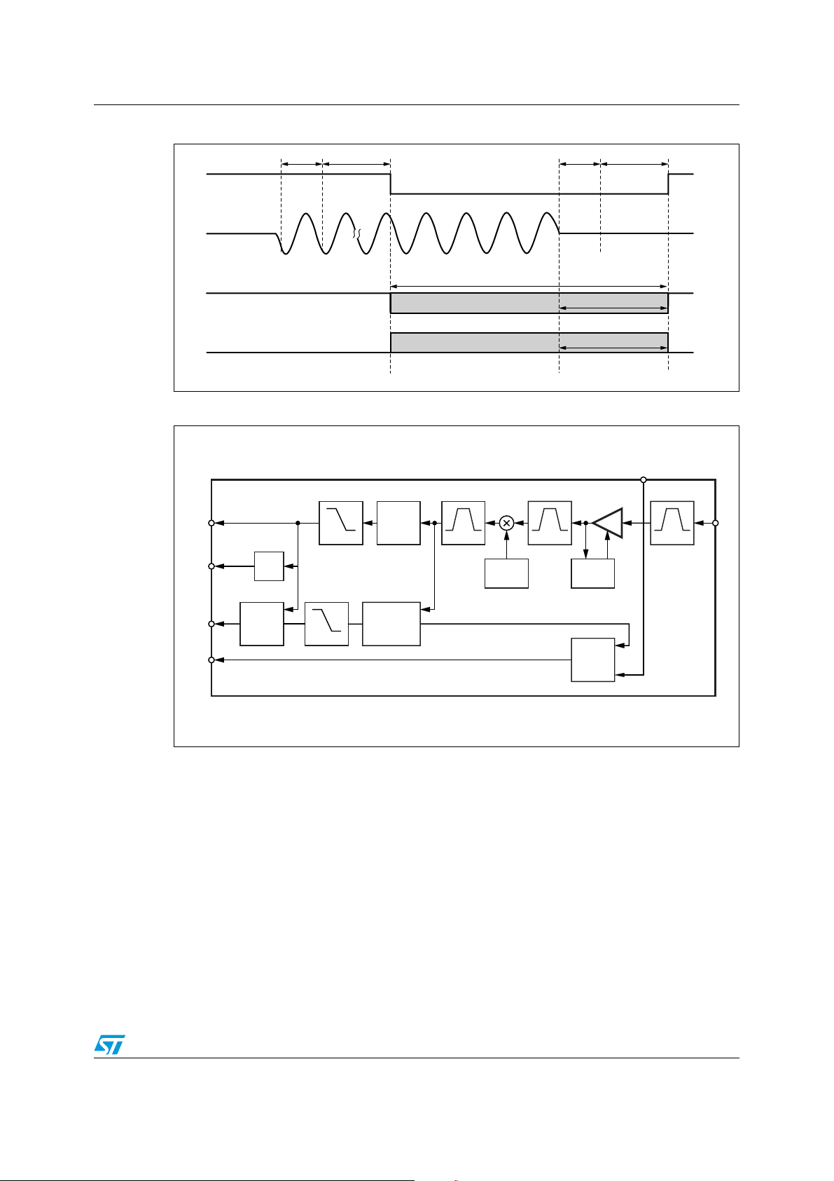
5.7.3 Carrier/preamble detection
The Carrier/Preamble Block is a digital Frequency detector Circuit.
It can be used to manage the MAINS access and to detect an incoming signal.
Two are the possible setting:
● Carrier detection: The Carrier/Preamble detection Block notifies to the host controller
the presence of a Carrier when it detects on the RAI Input a signal with an harmonic
component close to the programmed Carrier Frequency. The CD_PD signal sensitivity
is identical to the data reception sensitivity (0.5mVrms Typ. in Normal Sensitivity
Mode).
The CD_PD line is forced to a logic level low when a Carrier is detected.
● Preamble detection: The Carrier/Preamble detection Block notifies to the host
controller the presence of a Carrier modulated at the Programmed Baud Rate for at
least 4 Consecutive Symbols (“1010” or “0101” are the symbols sequences detected).
CD_PD line is forced low till a Carrier signal is detected and PLL is in the lock-in range.
To reinforce the effectiveness of the information given by CD_PD Block, a digital
filtering is applied on Carrier or Preamble notification signal (See Control Register
Paragraph). The Detection Time Bits in the Control Register define the filter
performance. Increasing the Detection Time reduces the false notifications caused by
noise on main line. The Digital filter adds a delay to CD_PD notification equal to the
programmed Detection Time. When the carrier frequency disappears, CD_PD line is
held low for a period equal to the detection time and then forced high. During this time
the some spurious data caused by noise can be demodulated.
5.7.4 Header recognition
In Extended Control Register Mode (Control Register bit 21 = ”1”, see Ta bl e 1 1 ) the CD_PD
line can be used to recognize if an header has been sent during the transmission. With
Header Recognition function enable (Control Register bit 18 = ”1”, see Ta bl e 11 ), CD_PD
line is forced low when a Frame Header is detected. If Frame Length Count function is
enabled, CD_PD is held low and a number of 16 bit word equal to the Frame Length
selected is sent to the host controller. In this case, CLR/T is forced to “0” and RxD is forced
to “0” or “1” (according the UART/SPI pin level) when Header has not been detected or after
the Frame Length has been reached.
If Frame Length Count function is disabled, an header recognition is signaled by forcing
CD_PD low for one period of CLR/T line. In this case, CLR/T and RxD signal are always
present, even if no header has been recognized.
24/44
Page 25
ST7538Q Functional description
8
Figure 11. CD_PD timing during RX
CD_PD
RAI
RxD (UART/SPI="1")
T
DCD
T
CD
T
DCD
T
CD
demodulation active on RxD pin
noise demodulated
RxD (UART/SPI="0")
Figure 12. Receiving path block diagram
RxD
CLR/T
CD_PD
BU
3
Bits 3-4 &14
8
1
9
PLL
Bits 18-21 & 24-47
HEADER
RECOGN.
Bits 3-4
Low Pass Band Pass
DIGITAL
FILTER
Bits 9-10
Low Pass
Bits 3-4 & 22
FSK
DEMODULATOR
Bits 12-13 & 22
CARRIER/
PREAMBLE
DETECTION
IF FILTER
Bits 0-2
MIXER
Band Pass
CHANNEL
LOCAL
Bits 0 -2
Carrier Detection
FILTER
OSC
noise demodulated
RXFO
31
AGC
GAIN
CONTROL
BAND
IN
USE
D03IN141
Bit 23
Band Pass
PRE-FILTER
D03IN1419
32
RAI
25/44
Page 26
Functional description ST7538Q
5.8 Transmission mode
The transmit mode is set when RxTx Pin = ”0” and REG_DATA Pin = ”0”. In transmitting
mode the FSK Modulator and the Power Line Interface are turned ON. The transmit Data
(TXD) enter synchronously or asynchronously to the FSK modulator.
● Host Controller Synchronous Communication Mode: on CLR/T rising edge, TXD Line
Value is read and sent to the FSK Modulator. ST7538Q Manages the Transmission
timing according to the BaudRate Selected
● Host Controller Asynchronous Communication Mode: TXD data enter directly to the
FSK Modulator.The Host Controller Manages the Transmission timing
In both conditions no Protocol Bits are added by ST7538Q.
The FSK frequencies are synthesized in the FSK modulator from a 16MHz crystal oscillator
by direct digital synthesis technique. The frequencies Table in different Configuration is
reported in Ta bl e 7. The frequencies precision is same as external crystal one’s.
In the analog domain, the signal is filtered in order to reduce the output signal spectrum and
to reduce the harmonic distortion. The transition between a symbol and the following is done
at the end of the on-going half FSK sinewave cycle.
Figure 13. Transmitting path block diagram
TOUT
TxD
ZCOUT
Bit 7 & 8
TIMER
7
THERMAL
SENSOR
Bit 14
5
D-TYPE
FLIP
FLOP
8
15
Bit 0-5
DAC
FSK
MODULATOR
ZERO CROSSING
CLR/T GENERATOR
Bit 0-2
ALC
Band Pass
TRANSMISSION
FILTER
16
ZCIN
Bits 17 & 21
VOLTAGE
LOOP
CURRENT
LOOP
PLI
PLI
D03IN1420
29
Vsense
23
CL
19
ATOP1
21
ATOP2
24
ATOCLR/T
26/44
Page 27
ST7538Q Functional description
5.8.1 Automatic Level Control (ALC)
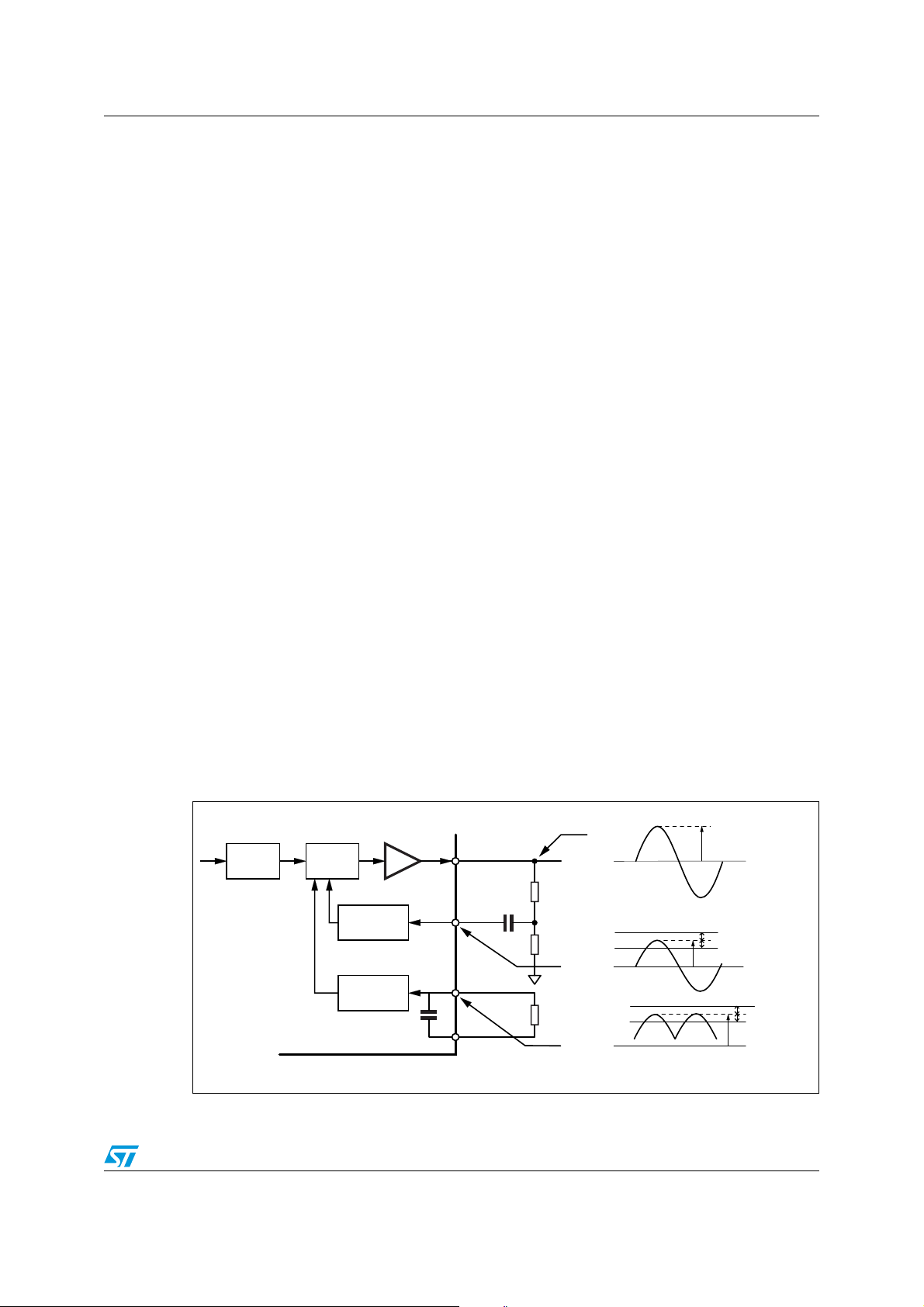
The Automatic Level Control Block (ALC) is a variable gain amplifier (with 32 non linear
discrete steps) controlled by two analog feed backs acting at the same time. The ALC gain
range is 0dB to 30 dB and the gain change is clocked at 5KHz. Each step increases or
reduces the voltage of 1dB (Typ).
Two are the control loops acting to define the ALC gain:
● The Voltage control loop acts to keep the Peak-to-Peak Voltage constant on Vsense.
The gain adjustment is related to the result of a peak detection between the Voltage
waveform on Vsense and two internal Voltage references. It is possible to protect the
Voltage Control Loop against noise by freezing the output level (see Section 6.6:
Output voltage level freeze on page 38).
If Vsense < VCL
If VCL
TH
- VCL
If Vsense > VCL
● The Current control loop acts to limit the maximum Peak Output current inside
- VCL
TH
HYST
TH
HYST
< Vsense < VCLTH + VCL
+ VLC
The next gain level is decreased by 1 step
HYST
The next gain level is increased by 1 step
HYST
No Gain Change
ATOP1 and ATOP2.
The current control loop acts through the voltage control loop decreasing the Output
Peak-to-Peak Amplitude to reduce the Current inside the Power Line Interface.
The current sensing is done by mirroring the current in the High side MOS of the Power
Amplifier (not dissipating current Sensing). The Output Current Limit (up to
400mApeak), is set by means of an external resistor (R
) connected between CL and
CL
PAVss. The resistor converts the current sensed into a voltage signal. The Peak current
sensing block works as the Output Voltage sensing Block:
If V(CL) < CCL
If CCL
TH
- CCL
If V(CL) > CCL
- CCL
TH
HYST
TH
HYST
< V(CL) < CCLTH + CCL
+ CLC
HYST
Voltage Control Loop Acting
HYST
No Gain Change
The next gain level is decreased by 1 step
Figure 14 shows the typical connection of Current an Voltage control loops.
Figure 14. Voltage and current feedback external interconnection example
VR
PK
ALC
ATOP/ATO
Vout
VOLTAGE
LOOP
CURRENT
LOOP
80 pF
D03IN1421
R1
Vsense
VCL
VCL
TH
HYST
1.865V (Typ)
CCL
CCL
TH
HYST
CL
AVss
5.6nF
RCL
R2
27/44
Page 28
Functional description ST7538Q
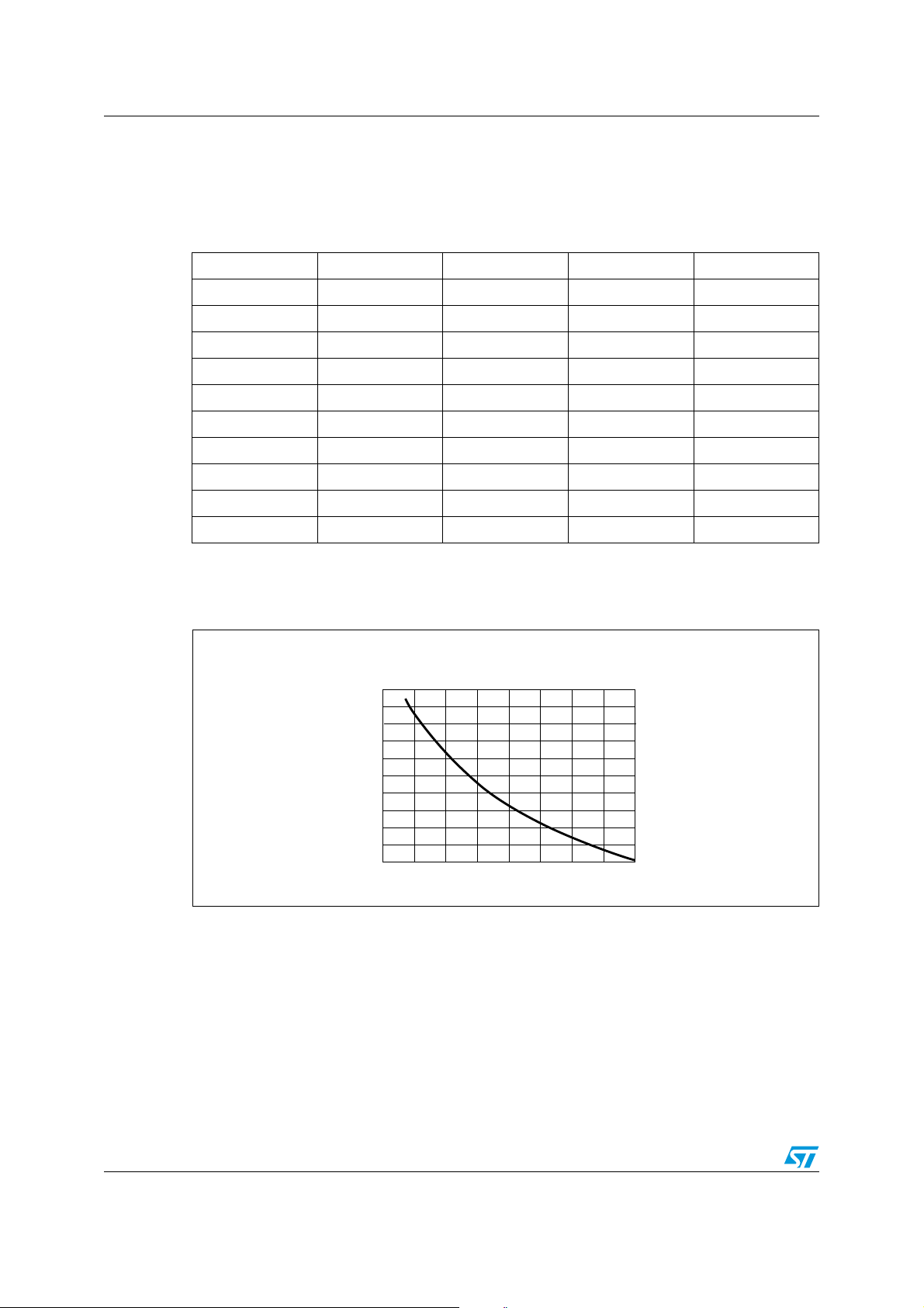
Voltage control loop formula
R1R2+
PK
--------------------
R
2
VCL
TH
±()⋅≅
VCL
HYST
VR
Table 10. Vout vs R1 & R2 resistors value
Vout (V r m s ) Vout ( d B µV) (R1+R2)/R2 R2 (KΩ) R1 (KΩ)
0.150 103.5 1.1 7.5 1.0
0.250 108.0 1.9 5.1 3.9
0.350 110.9 2.7 3.6 5.6
0.500 114.0 3.7 3.3 8.2
0.625 115.9 4.7 3.3 11.0
0.750 117.5 5.8 2.7 12.0
0.875 118.8 6.6 2.0 11.0
1.000 120.0 7.6 1.6 10.0
1.250 121.9 9.5 1.6 13.0
1.500 123.5 10.8 1.6 15.0
Note: The rate of R2 takes in account the input resistance on the SENSE pin (36 K
5.6nF capacitor effect has been neglected.
Figure 15. Typical output current vs rcl
Irms
(mA)
325
300
275
250
225
200
175
150
125
100
2 2.5 3 3.5
4 4.5 5
D01IN1311
Rcl(KΩ)
Ω
).
28/44
Page 29
ST7538Q Functional description
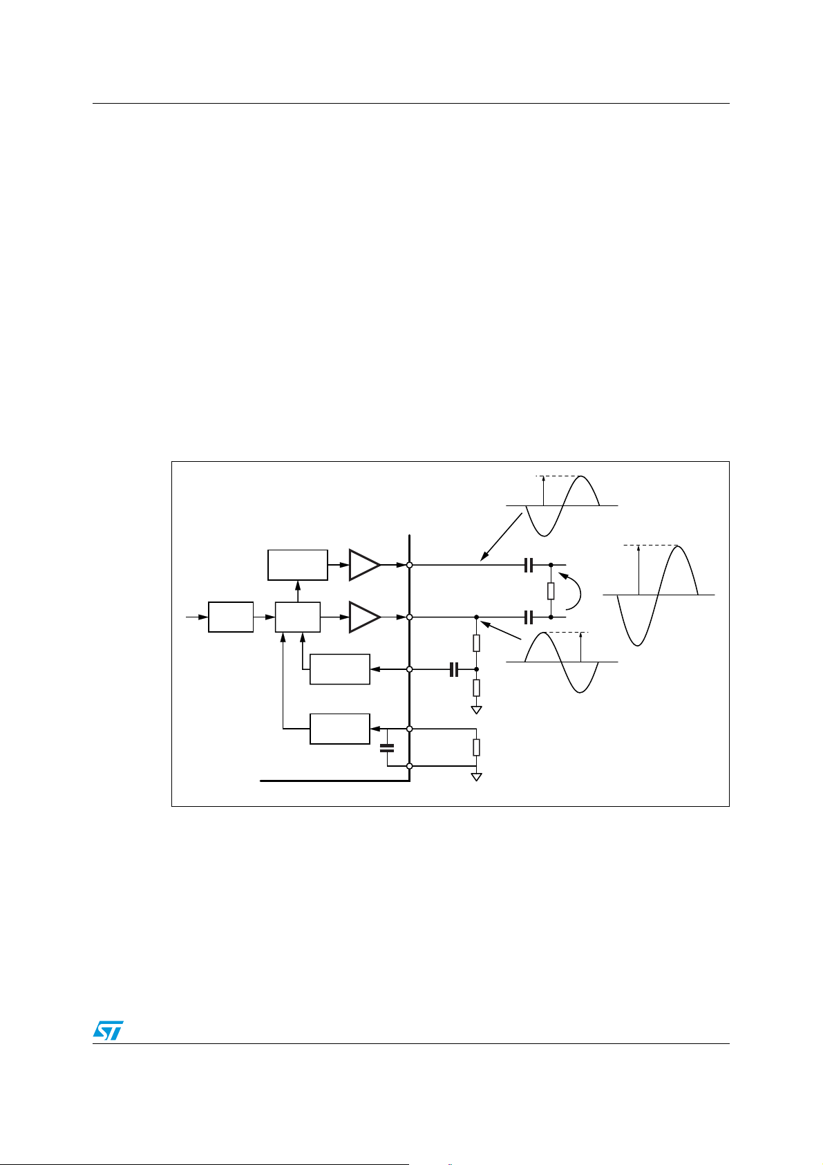
● Integrated Power Line Interface (PLI)
The Power Line Interface (PLI) is a double CMOS AB Class Power Amplifier with the
two outputs (ATOP1 and ATOP2) in opposition of phase.
Two are the possible configuration:
- Single Ended Output (ATOP1).
- Bridge Connection
The Bridge connection guarantee a Differential Output Voltage to the load with twice
the swing of each individual Output. This topology virtually eliminates the even
harmonics generation.
The PLI requires, to ensure a proper operation, a regulated and well filtered Supply
Voltage. PAVcc Voltage must fulfil the following formula to work without clipping
phenomena:
PAVcc
VATOP AC()
------------------------------- ---- - 7.5V+≥
2
To allow the driving of an external Power Line Interface, the output of the ALC is
available even on ATO pin. ATO output has a current capability much lower than ATOP1
and ATOP2.
Figure 16. PLI bridge topology
VR
PK
INVERTER
ALC
VOLTAGE
LOOP
CURRENT
LOOP
80 pF
D03IN1422
ATOP2
ATOP1
Vsense
CL
PAVss
5.6nF
RCL
R1
R2
Vout
LOAD
VR
2*VR
PK
PK
29/44
Page 30
Functional description ST7538Q
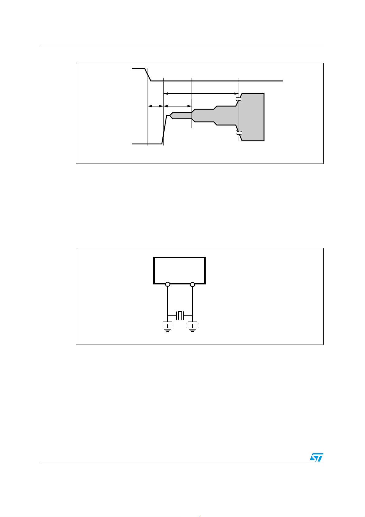
Figure 17. PLI startup timing diagram
RX/TX
T
ALC
ATOP2
5.9 Crystal oscillator
ST7538Q integrates a inverter driver circuit to realize a 16MHz crystal oscillator.
This circuit is able to drive a maximum load capacitance of 16pF with typical quartz ESR of
40Ω.
If the internal driver circuit is used, only one external crystal quartz and two external load
capacitors (C
Figure 18. Typical crystal configuration if internal crystal driver circuit is used
and C2) are needed to realize the oscillator function (Figure 18).
1
4V
0V
T
ST
D03IN1408
T
RXTX
STEP NUMBER 16 17 18 31
XOUT XIN
C
1
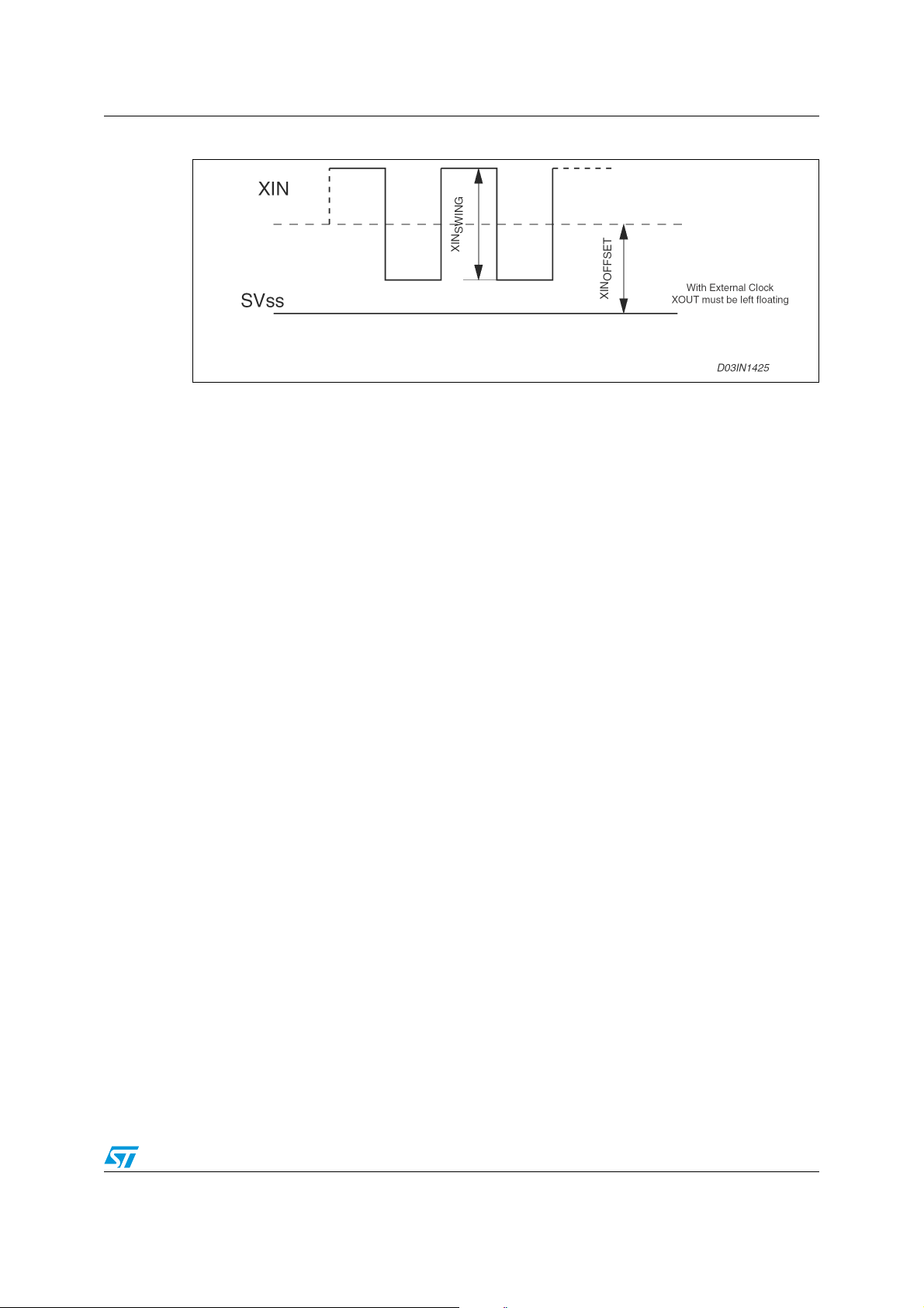
If an external oscillator is used, XOUT must be disconnected, while XIN must satisfies the
specifications given in Ta bl e 4 (see Figure 19).
30/44
C
2
D03IN1425A
Page 31
ST7538Q Functional description
Figure 19. XIN waveform if an external oscillator is used
5.10 Control register
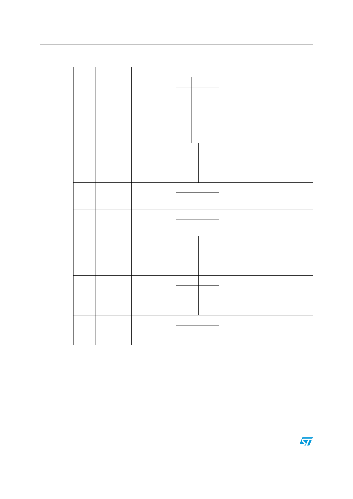
The ST7538Q is a multi-channel and multifunction transceiver. An internal 24 or 48 Bits (in
Extended mode) Control Register allows to manage all the programmable parameters
(Ta bl e 11 ).
The programmable functions are:
● Channel Frequency
● Baud Rate
● Deviation
● Watchdog
● Transmission Timeout
● Frequency Detection Time
● Detection Method
● Mains Interfacing Mode
● Output Clock
● Sensitivity Mode
● Input Pre-Filter
In addition to these functions the Extended mode provides 24 additional bits and others
functions:
● Output Level Freeze
● Frame Header Recognizer (one 16 bits header of or two 8 bits headers) with support to
Frame Length Bit count
31/44
Page 32
Functional description ST7538Q
Table 11. Control register functions
Bits Function Value Selection Note Default
Bit2 Bit1 Bit0
0 to 2 Frequencies
3 to 4 Baud Rate
5Deviation
6 Watchdog
7 to 8
9 to 10
Transmission
Time Out
Frequency
detection
time
60 KHz
66 KHz
72 KHz
76 KHz
82.05 KHz
86 KHz
110 KHz
132.5 KHz
600
1,200
2,400
4,800
0.5
1
Disabled
Enabled (1.5 s)
Disabled
1 s
3 s
Not Used
500 µs
1 ms
3 ms
5 ms
0
0
0
0
0
1
0
1
1
0
1
0
1
1
1
1
Bit 4 Bit 3
0
0
1
1
Bit 8 Bit 7
0
0
1
1
Bit 10 Bit 9
0
0
1
1
0
1
0
1
Bit 5
0
1
Bit 6
0
1
0
1
0
1
0
1
0
1
0
1
0
1
0
1
0
1
132.5 kHz
2400
0.5
Enabled
1 sec
1 ms
Zero
11
32/44
Crossing
Synchronizati
on
Disabled
Enabled
Bit 11
0
1
Disabled
Page 33
ST7538Q Functional description
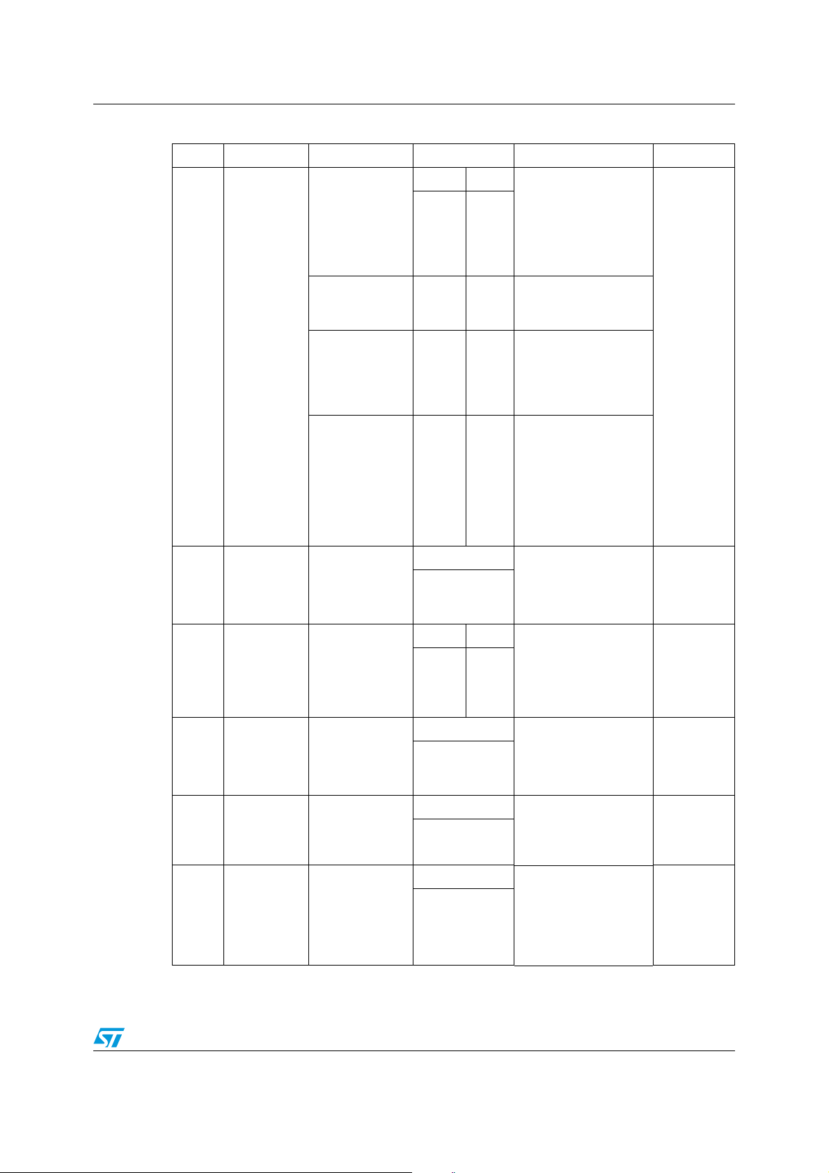
Table 11. Control register functions (continued)
Function Value Selection Note Default
Bit 13 Bit 12
Carrier Detection
Carrier detection
without
conditioning
00
Notification on CD_PD
Line
CLR/T and RxD signal
always Present
12 to
13
14
15 to
16
17
Detection
(1)
Method
Mains
Interfacing
Mode
Output Clock
Output
Voltage Level
Freeze
Carrier detection
with conditioning
Preamble
detection
without
conditioning
Preamble
detection
with conditioning
Synchronous
Asynchronous
16 MHz
8 MHz
4 MHz
Clock OFF
Enabled
Disabled
01
10
11
Bit 14
0
1
Bit 16 Bit 15
0
0
1
1
0
1
0
1
Bit 17
0
1
CLR/T and RxD lines
are forced to “0” when
Carrier is not detected
Preamble Detection
Notification on CD_PD
Line
CLR/T and RxD signal
always Present
Preamble Detection
Notification on CD_PD
Line
CLR/T and RxD lines
are forced to “0” when
Preamble has not been
detected or PLL is in
Unlock condition
Active only if Extended
Control Register is
enable (Bit 21=”1”)
Preamble
detection
without
conditioning
Asynchronou
s
4 MHz
Disabled
18
19
Header
Recognition
Frame
Length Count
Disabled
Enabled
Disabled
Enabled
Bit 18
0
1
Bit 19 Active only if Header
0
1
33/44
Active only if Extended
Control Register is
enable (Bit 21=”1”)
Recognition Function
(Bit 18=”1”) and
Extended Control
Register (Bit 21=”1”)
are enable
Disabled
Disabled
Page 34
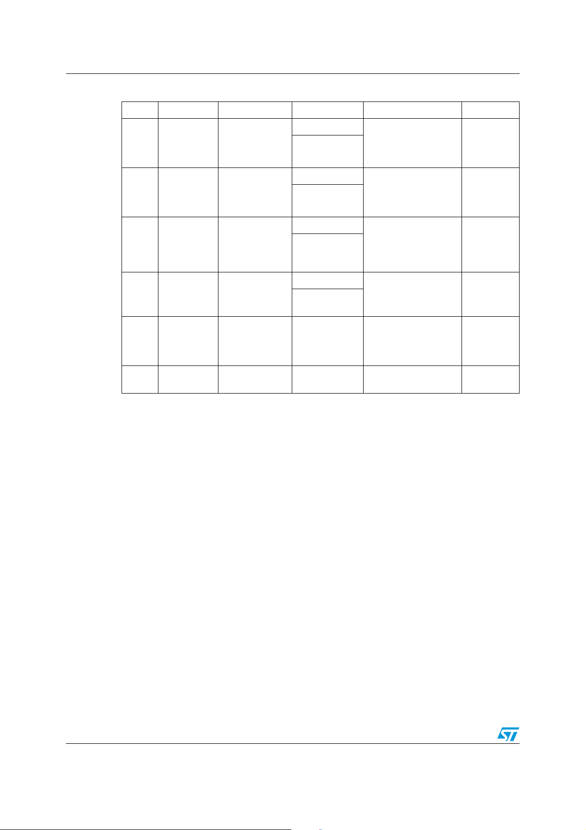
Functional description ST7538Q
Table 11. Control register functions (continued)
Function Value Selection Note Default
Bit 20
Active only if Extended
Control Register is
enable (Bit 21=”1”)
Extended Register
enables Functions on
Bit 17, 18,19 and 20
16 bits
Disabled
(24 bits)
20
21
Header
Length
Extended
Register
8 bits
16 bits
Disable (24 bits)
Enabled (48 bits)
0
1
Bit 21
0
1
Bit 22
Normal
Sensitivity
High Sensitivity
0
1
Normal
22
Sensitivity
Mode
Bit 23
23 Input Filter
Disabled
Enabled
0
Disabled
1
One 16 bits Header or
24 to
39
Frame
Header
from 0000h to
FFFFh
two 8 bits Headers
(MSB first) depending
9B58h
on Bit 17
40 to
47
1. The Detection method bit meaning differs depending on UART/SPI pin value. In this table is listed the SPI
mode (UART/SPI=”0”). For Detection method bit meaning in UART mode (UART/SPI=”1”) please see
Table 12.
Frame
Length
from 01h to FFh
Number of 16 bits
words expected
08h
34/44
Page 35
ST7538Q Functional description
5.11 Detection method and Rx Sensitivity in UART mode
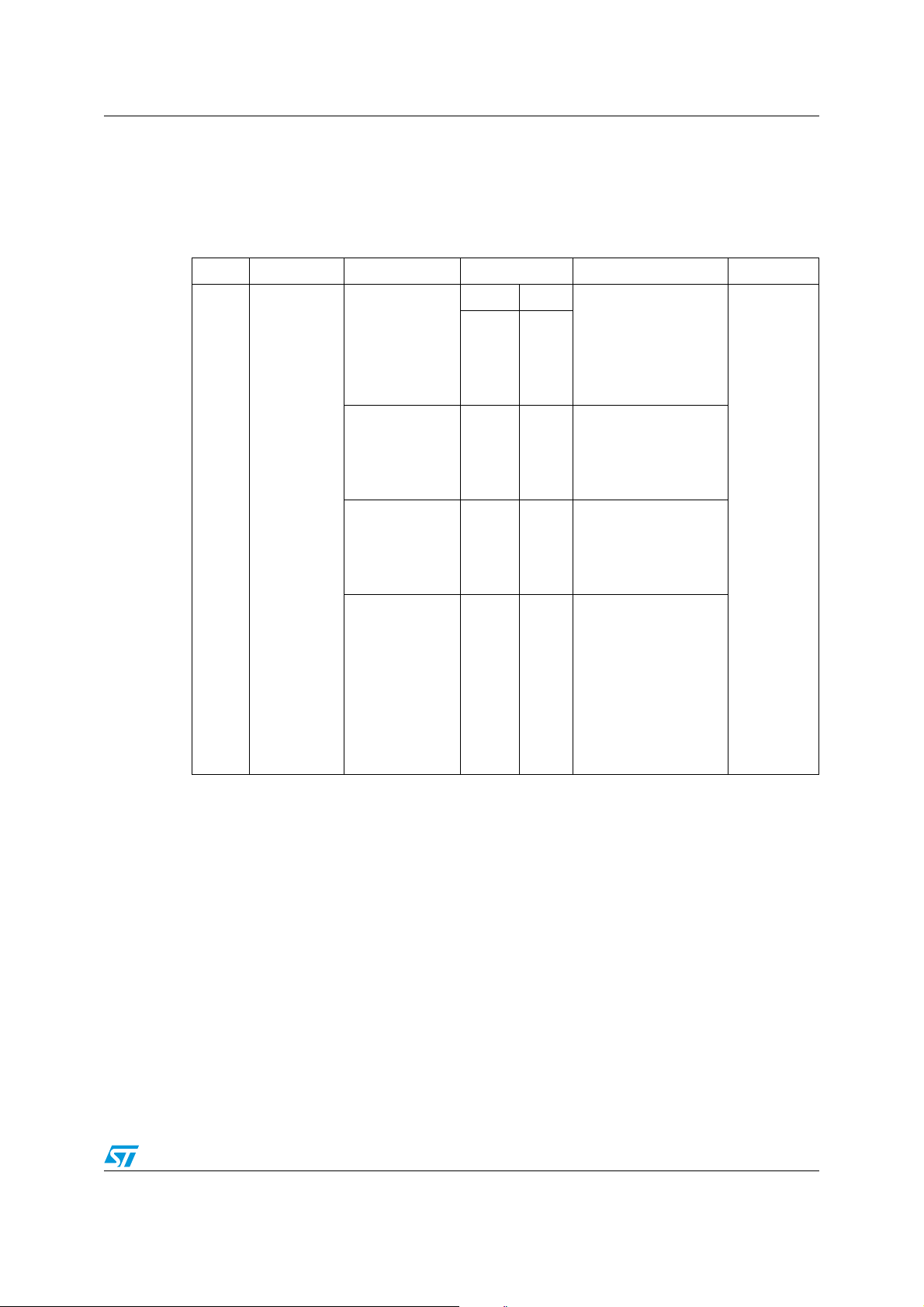
When ST7538Q is running in UART mode (by forcing UART/SPI pin to “1”) the Control
Register Function “Detection method” differs from SPI mode as indicated in the Tab le 1 2:
Table 12. Control register functions in UART mode
Function Value Selection Note Default
Bit 13 Bit 12
This configuration
should be avoided
Not Allowed 0 0
Not Allowed 0 1
because it could cause
an unpredictable
behavior of the device
This configuration
should be avoided
because it could cause
an unpredictable
behavior of the device
12 to 13Detection
Method
Carrier detection
without
conditioning
Carrier detection
with conditioning
Notification on CD_PD
10
CLR/T and RxD signal
Notification on CD_PD
CLR/T Line is forced to
11
Carrier Detection
Line
always Present
Carrier Detection
Line
“0” and RxD Line is
forced to “0” or “1”
(according the
UART/SPI pin level)
when Carrier is not
detected
Carrier
detection
without
conditioning
UART mode provides also a third level of Receiving sensitivity in addition to two levels select
able by Control Register (see Tab le 1 1). By setting to “1” the TxD pin during a receiving
session the sensitivity is forced to BU threshold (this condition suppresses the Control
Register setting).
35/44
Page 36
Auxiliary analog and digital functions ST7538Q
6 Auxiliary analog and digital functions
6.1 Band in use
The Band in Use Block has a Carrier Detection like function but with a different Input
Sensibility (77dBµV Typ.)
and with a different BandPass filter Selectivity (40dB/Dec).
BU line is forced High when a signal in band is detected.
To prevent BU line false transition, BU signal is conditioned to Carrier Detection Internal
Signal.
6.2 Time out
Time Out Function is a protection against a too long data transmission. When Time Out
function is enabled after 1 or 3 second of continuos transmission the transceiver is forced in
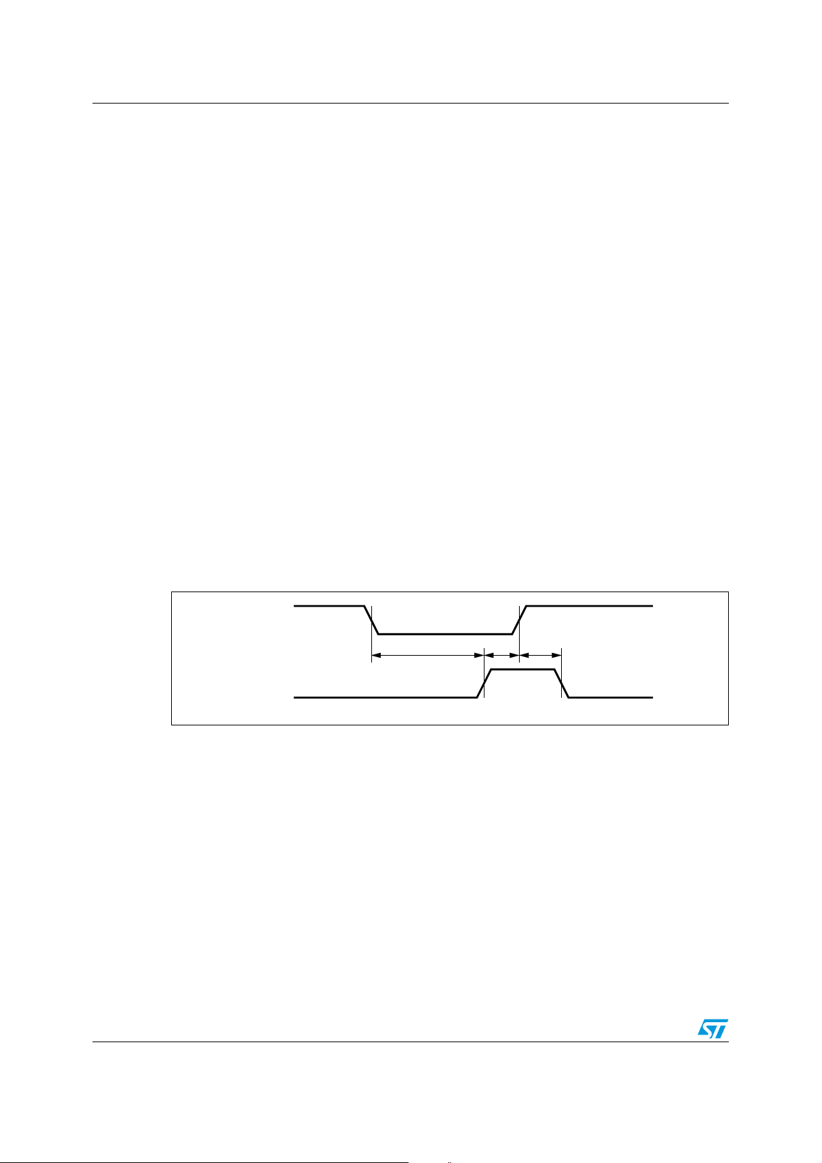
receiving mode. This function allows ST7538Q to automatically manage the CENELEC
Medium Access specification. When a time-out event occur, TOUT is forced high, and is
held high for at least 125 ms. To Unlock the Time Out condition RxTx should be forced High.
During the time out period only register access or reception mode are enabled.
During Reset sequence if RxTx line =”0” & REG_DATA line =”0”, TIMEOUT protection is
suddendly enabled and ST7538Q must be configured in data reception after the reset event
before starting a new data transmission.
Time Out time is programmable using Control Register bits 7 and 8 (Ta b le 1 1).
Figure 20. Time-out timing and unlock sequence
RxTx
Time Out function
6.3 Reset & watchdog
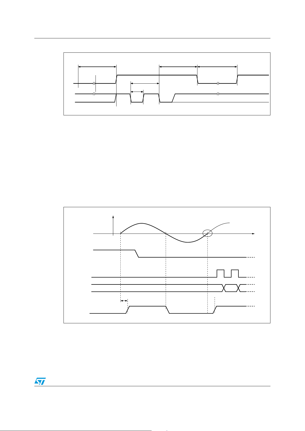
RSTO Output is a reset generator for the application circuitry. During the ST7538Q startup
sequence is forced low. RSTO becomes high after a T
startup sequence.
Inside ST7538Q is also embedded a watchdog function. The watchdog function is used to
detect the occurrence of a software fault of the Host Controller. The watchdog circuitry
generates an internal and external reset (RSTO low for T
watchdog timer. The watchdog timer reset can be achieved applying a negative pulse on
WD pin (Figure 21).
T
OUT
T
OFFTOFFD
delay from the end of oscillator
RSTO
RSTO
D03IN1409
time) on expiry of the internal
36/44
Page 37
ST7538Q Auxiliary analog and digital functions
Figure 21. Reset and watchdog timing
T
RSTO
RSTO
T
WD
WD
6.4 Zero crossing detection
The Mains Voltage Zero Crossing can be detected, through a proper connection of ZCIN to
the Mains. ZCIN comparator has a threshold fixed at SGND. ZCOUT is a TTL Output forced
High after a positive zero-crossing transition, and low after a negative one.
Setting the Bit 11 inside the Control Register to “1” the transmission is automatically
synchronized to the mains positive zero-crossing transition. This function is achieved turning
on the PLI when RX/TX is low and delaying the CLR/T first transition until the first zerocrossing event. The automatic synchronization procedure can work only if the synchronous
interface is programmed. If asynchronous interface is in use the Zero Crossing
synchronization can be achieved managing the ZCOUT line.
Figure 22. Synchronous zero-crossing transmission
T
WO
T
WM
T
RSTO
D03IN1410
ZCIN
RxTx
CLR/T
TxD
ZCOUT
t
ZC
DEL
D03IN1423
37/44
Page 38

Auxiliary analog and digital functions ST7538Q
6.5 Output clock
MCLK is the master clock output. The clock frequency sourced can be programed through
the control register to be a ratio of the crystal oscillator frequency (Fosc, Fosc/2 Fosc/4) or
can be disabled (off). The transition between one frequency and another is done only at the
end of the ongoing cycle.
6.6 Output voltage level freeze
The Output Level Freeze function, when enabled, turns off the Voltage Control Loop once
the ALC stays in a stable condition for about 3 periods of control loop, and maintains a
constant gain until the end of transmission. Output Level Freeze can be enabled using
Control Register bit 17 (Ta bl e 1 1). This function is available only using the Extended Control
Register (Control Register bit 21 = ”1”).
6.7 Extended control register
When Extended Control Register function is enabled, all the 48 bits of Control Register are
programmable. Otherwise, only the first 24 bits of Control Register are programmable. The
functions Header Recognition, Frame Bit Count and Output Voltage Freeze are available
only if Extended Control Register function is enabled. Extended Control Register can be
enabled setting the Control Register bit 21(Ta bl e 11 ).
6.8 Reg OK
REGOK allows to detect an incomplete writing of the Control Register content (see
Section 5.6: Control register access on page 21) or an accidental corruption of the Control
Register content. In these cases REGOK goes to “1” until a new Control Register writing
session is performed.
6.9 Under voltage lock out
The UVLO function turns off the device if the PAVcc voltage falls under 4V. Hysteresis is
340mV typically.
6.10 Thermal shutdown
The ST7538Q is provided of a thermal protection which turn off the PLI when the junction
temperature exceeds 170°C ± 10% . Hysteresis is around 30°C.
When shutdown threshold is overcome, PLI interface is switched OFF.
Thermal Shutdown event is notified to the HOST controller using TIMEOUT line. When
TIMEOUT line is High, ST7538Q junction temperature exceed the shutdown threshold (Not
Leached).
38/44
Page 39
ST7538Q Auxiliary analog and digital functions
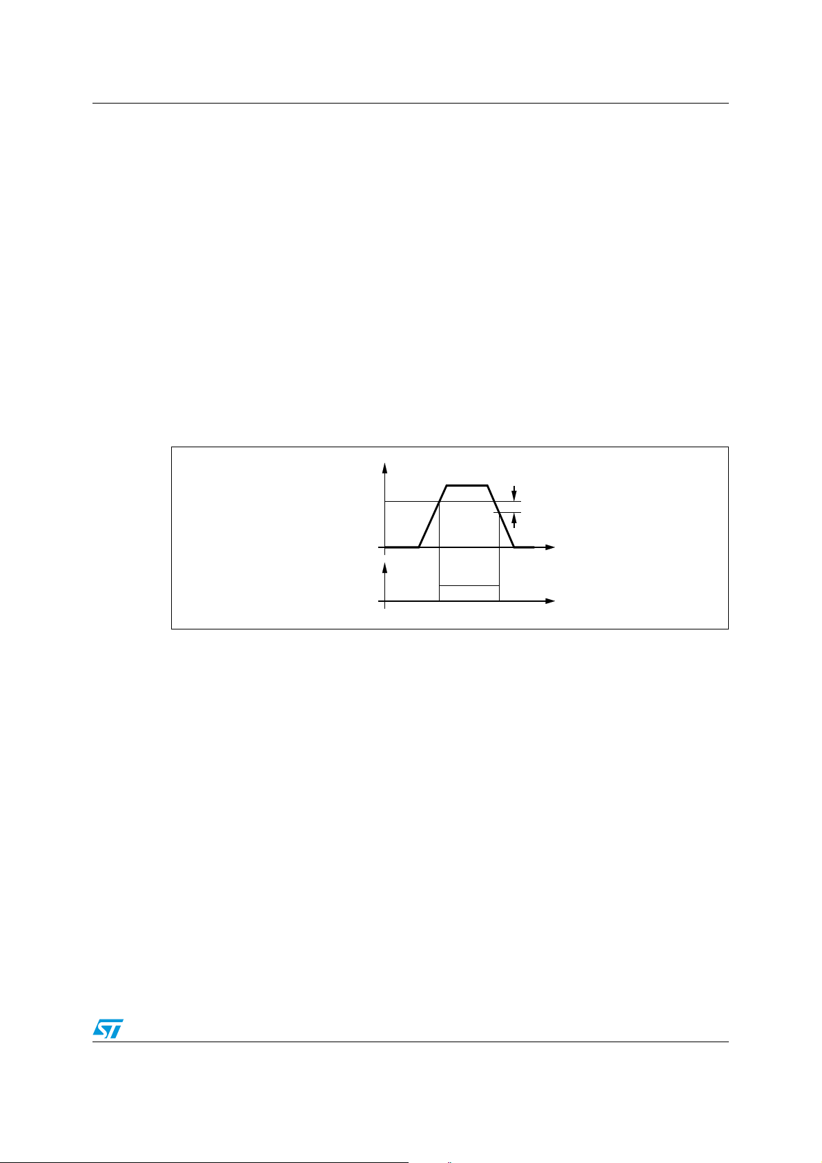
6.11 5V and 3.3V voltage regulators and power good function
ST7538Q has an embedded 5V linear regulator externally available to supply the application
circuitry.
The linear regulator has a very low quiescent current (50µA) and a current capability of
50mA. The regulator is protected against short circuitry events.
The DVdd pin can act either as 3.3V Voltage Output or as Input Digital Supply. When the
DVdd pin is externally forced to 5V all the Digital I/Os operate at 5V, otherwise all the Digital
I/Os are internally supplied at 3.3V. The DVdd pin can also source 3.3V voltage to supply
external components. The 3.3V linear regulator has a very low quiescent current (50µA) and
a current capability of 50mA. The regulator is protected against short circuitry events.
If AVdd and DVdd pins are connected to VDC pin, the 5V regulator maximum current
capability rises to 100mA
When the regulator Voltages are above of the power good thresholds V
(see Ta bl e 4 ),
PG
Power Good line is forced high, while is forced low at startup and when VDC or DVdd falls
below V
PG
- V
PGHYS
Voltage.
Figure 23. Power good function
VDC/DV
DD
4.5V/3.125V
250mV
Time
PG
PG OK
D03IN1411
Time
39/44
Page 40
Auxiliary analog and digital functions ST7538Q
6.12 Power-up procedure
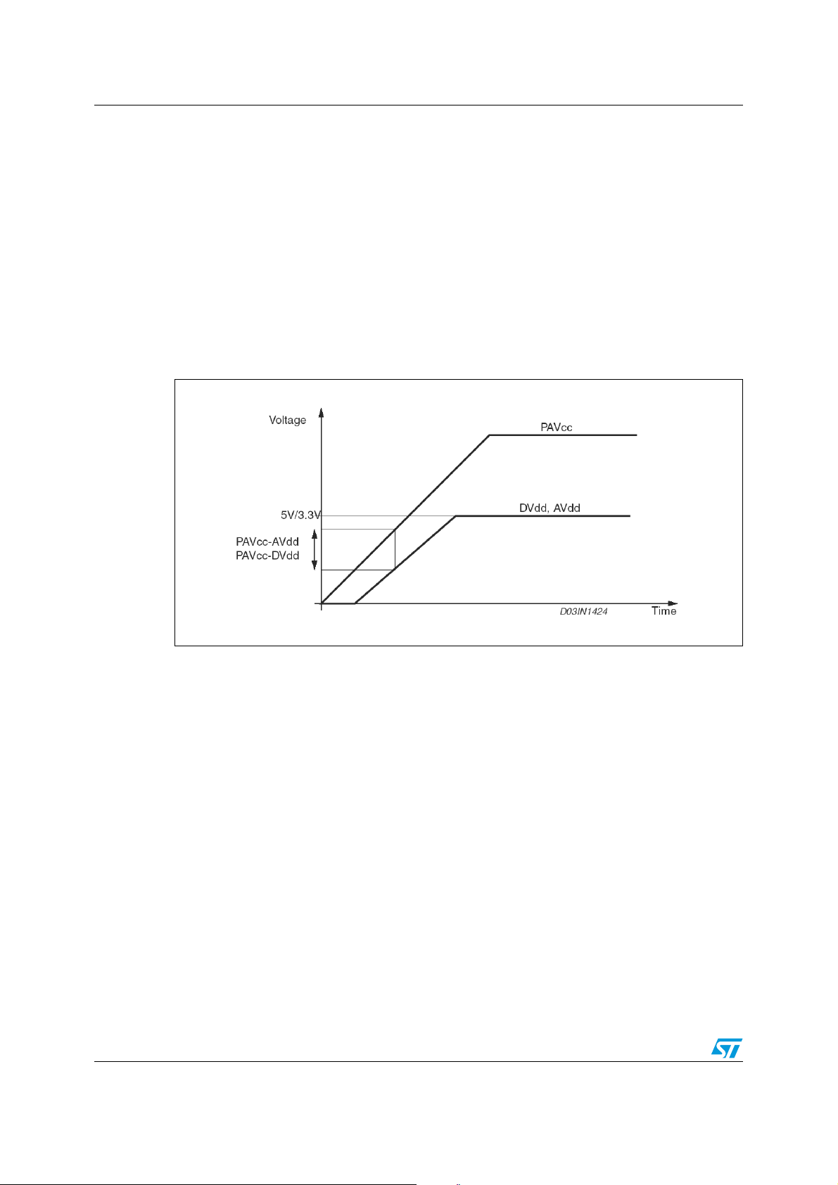
To ensure ST7538Q proper power-Up sequence, PAVcc, AVdd and DVdd Supply has to fulfil
the following rules:
PAVcc rising slope must not exceed 100V/ms.
When DVdd is below 5V/3.3V and AVdd is below 5V: 100mV < PAVcc-AVdd , PAVcc-DVdd <
1.2V.
When AVdd and DVdd supplies are connected to VDC the above mentioned relation is
guarantied if VDC load < 100mA and if the filtering capacitor on VDC < 100uF.
If DVdd is not forced to 5V, the Digital I/Os are internally supplied at 3.3 V and if DVdd load <
50mA and the filtering capacitor on DVdd < 100uF the second relation can be ignored .
Figure 24. Power-UP sequence
40/44
Page 41
ST7538Q Auxiliary analog and digital functions
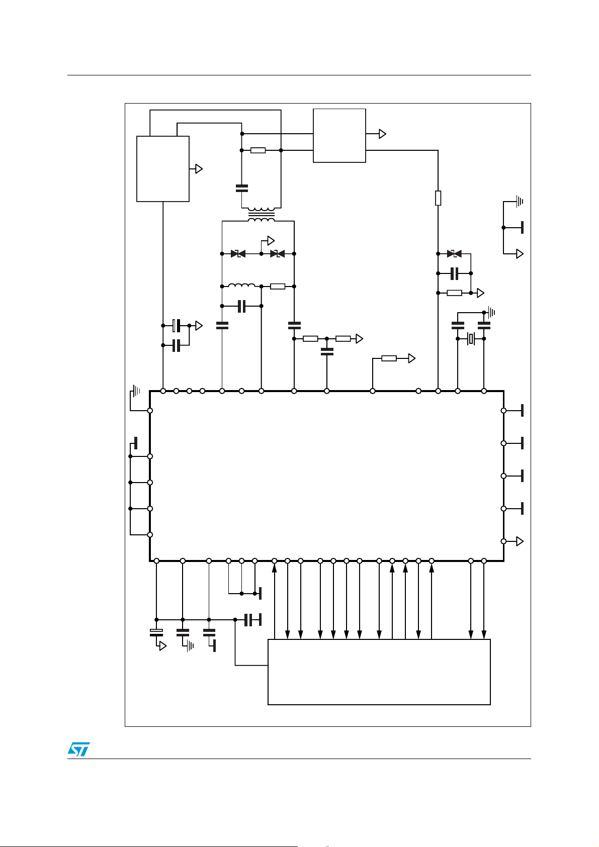
Figure 25. Application schematic example with coupling tranformer.
circuit
Mains
Coupling
reference
AC/DC
Converter
SINGLE SUPPY
PAVCC
22
25
SGND
17
N.C.
34
N.C.
39
N.C.
44
33
N.C.
VDC
C_OUT40
AVdd
C_PLUS38C_MINUS37
28
No External Components
for POWER LINE DRIVER
ATOP2
ATO24
21
10
13
30
DVdd
TEST235TEST1
UART/SPI
RAI
32
AC LINE
LOAD
WD
ATOP1
143642
PG
R1
19
REGOK
Voltage
R2
C1
Vsense
29
ST7538Q
789
15
BU
TOUT
ZCOUT
&
Current
Protection
Regulation
CL
23
1
345
RxD
CD/PD
RCL
TxD
CLR/T
RX/TX
RxFO31
REG/DATA
Transmission
Zero Crossing
XIN27XOUT
ZCIN
16
43
5 Lines
Serial Interface
Synchronization
26
41
6
2
1820
11
12
RSTO
MCLK
Host Controller
Clock & Reset for
D03IN1412A
GND
DVSS GND
DVSS
PAVSS
5V Supply
for Host Controller
HOST
CONTROLLER
41/44
Page 42
Package mechanical data ST7538Q
3
7 Package mechanical data
In order to meet environmental requirements, ST offers these devices in ECOPACK®
packages. These packages have a Lead-free second level interconnect . The category of
second level interconnect is marked on the package and on the inner box label, in
compliance with JEDEC Standard JESD97. The maximum ratings related to soldering
conditions are also marked on the inner box label. ECOPACK is an ST trademark.
ECOPACK specifications are available at: www.st.com
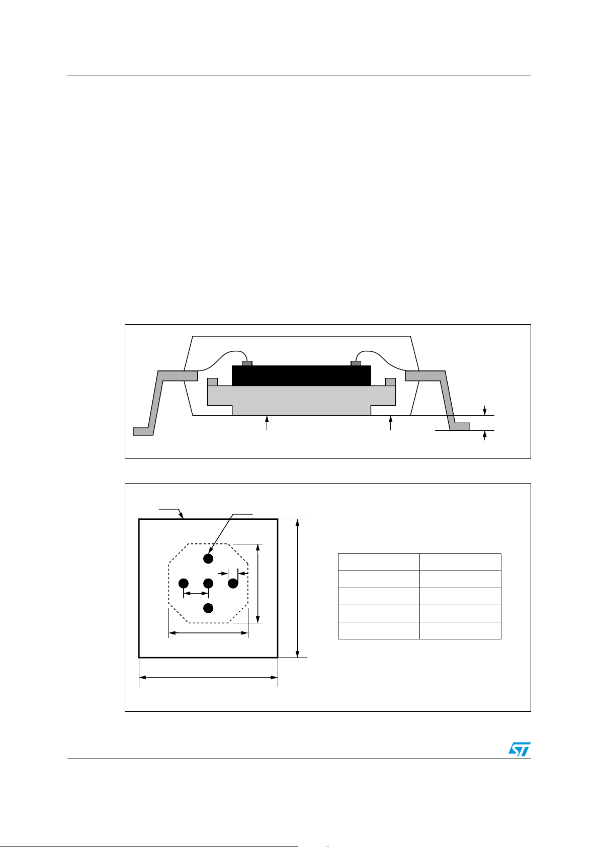
Best thermal performance is achieved when slug is soldered to PCB.
It is recommended to have five solder dots (See Figure 27) without resist to connect the
Copper slug to the ground layer on the soldering side. Moreover it is recommitted to connect
the ground layer on the soldering side to another ground layer on the opposite side with 15
to 20 vias.
It is suggested to not use the PCB surface below the slug area to interconnect any pin
except ground pins.
Figure 26. ST7538Q slug drawing
Copper Slug
Solder plated
Figure 27. Soldering information
Cu plate
A
Solder dots
B
L
L
L1
L1
D03IN141
0.10mm ±0.05
Lead frame
D03IN1414
Package Sizes 10x10x1.4mm
A 2.00 mm
B 1.00 mm
L 6.00 mm
L1 (Copper plate) 10.00 mm
If PCB with ground layer, connect
copper plate with 15 to 20 vias
42/44
Page 43
ST7538Q Revision history
8 Revision history
Table 13. Revision history
Date Revision Changes
12-Jul-2006 1 Initial release.
43/44
Page 44

ST7538Q
Please Read Carefully:
Information in this document is provided solely in connection with ST products. STMicroelectronics NV and its subsidiaries (“ST”) reserve the
right to make changes, corrections, modifications or improvements, to this document, and the products and services described herein at any
time, without notice.
All ST products are sold pursuant to ST’s terms and conditions of sale.
Purchasers are solely responsible for the choice, selection and use of the ST products and services described herein, and ST assumes no
liability whatsoever relating to the choice, selection or use of the ST products and services described herein.
No license, express or implied, by estoppel or otherwise, to any intellectual property rights is granted under this document. If any part of this
document refers to any third party products or services it shall not be deemed a license grant by ST for the use of such third party products
or services, or any intellectual property contained therein or considered as a warranty covering the use in any manner whatsoever of such
third party products or services or any intellectual property contained therein.
UNLESS OTHERWISE SET FORTH IN ST’S TERMS AND CONDITIONS OF SALE ST DISCLAIMS ANY EXPRESS OR IMPLIED
WARRANTY WITH RESPECT TO THE USE AND/OR SALE OF ST PRODUCTS INCLUDING WITHOUT LIMITATION IMPLIED
WARRANTIES OF MERCHANTABILITY, FITNESS FOR A PARTICULAR PURPOSE (AND THEIR EQUIVALENTS UNDER THE LAWS
OF ANY JURISDICTION), OR INFRINGEMENT OF ANY PATENT, COPYRIGHT OR OTHER INTELLECTUAL PROPERTY RIGHT.
UNLESS EXPRESSLY APPROVED IN WRITING BY AN AUTHORIZED ST REPRESENTATIVE, ST PRODUCTS ARE NOT
RECOMMENDED, AUTHORIZED OR WARRANTED FOR USE IN MILITARY, AIR CRAFT, SPACE, LIFE SAVING, OR LIFE SUSTAINING
APPLICATIONS, NOR IN PRODUCTS OR SYSTEMS WHERE FAILURE OR MALFUNCTION MAY RESULT IN PERSONAL INJURY,
DEATH, OR SEVERE PROPERTY OR ENVIRONMENTAL DAMAGE. ST PRODUCTS WHICH ARE NOT SPECIFIED AS "AUTOMOTIVE
GRADE" MAY ONLY BE USED IN AUTOMOTIVE APPLICATIONS AT USER’S OWN RISK.
Resale of ST products with provisions different from the statements and/or technical features set forth in this document shall immediately void
any warranty granted by ST for the ST product or service described herein and shall not create or extend in any manner whatsoever, any
liability of ST.
ST and the ST logo are trademarks or registered trademarks of ST in various countries.
Information in this document supersedes and replaces all information previously supplied.
The ST logo is a registered trademark of STMicroelectronics. All other names are the property of their respective owners.
© 2006 STMicroelectronics - All rights reserved
STMicroelectronics group of companies
Australia - Belgium - Brazil - Canada - China - Czech Republic - Finland - France - Germany - Hong Kong - India - Israel - Italy - Japan -
Malaysia - Malta - Morocco - Singapore - Spain - Sweden - Switzerland - United Kingdom - United States of America
www.st.com
44/44
 Loading...