

Page 1
Rev. 1.4
January 2000 1/71
ST72411R
8-BIT MCU WITH SMARTCARD INTERFACE, LCD DRIVER,
8-BIT TIMER, SAFE RESET AND SUPPLY MONITORING
PRODUCT PREVIEW
■ Memories
– 4K Program memory
(ROM/FLASH) with read-out protection
– In-Situ Programming (remote ISP) for FLASH
devices using Smartcard orstandard I/O lines
– 256-bytes RAM
■ Clock, Reset and Supply Management
– Power-on supply at Smartcard insertion
– Low supply voltage detection for battery
monitoring
– Smart Card withdrawal detection
– On-chip main clock source
– 3 Power saving modes
– Clock-out capability for synchronous and
asynchronous Smartcards
■ Smartcard Interface
– Smart Card Supply Supervisor with: 3V or 5V
voltage regulator and current overload protec-
tion
■ 15 I/O Ports
– 15 multifunctional bidirectional I/O lines with:
external interrupt capability (2 vectors), 2 al-
ternate function lines, 5 I/Os for ISO7816-3
Smartcard interface, 1 I/O for Smartcard with-
drawal detection
■ Display Driver
– LCD driver with 32 segment outputs and 4
backplane outputs able to drive up to 32x4
LCD displays
■ Timer
– One 8-bit timer with: 9-bit prescaler, selecta-
ble input frequency with external clock input
option and event output signal generation ca-
pability
■ Instruction Set
– 8-bit Data Manipulation
– 63 Basic Instructions
– 17 main Addressing Modes
– 8 x 8 Unsigned Multiply Instruction
– True Bit Manipulation
■ Development Tools
– Full hardware/software development package
Device Summary
TQFP64
14 x 14
Features ST72411R
Program memory - bytes 4K
RAM (stack) - bytes 256 (64)
Peripherals Smart Card supply interface, LCD Driver, 8-bit Timer
Operating Supply 4V to 6.6V (5.5V min. for 5V Smartcard power supply output)
CPU Frequency 3.58 MHz (7.16 MHz internal oscillator)
Temperature Range 0°C to +70°C
Packages TQFP64 or Die Form
Development device ST72C411R
1
Page 2

Table of Contents
71
2/71
2
1 GENERAL DESCRIPTION . . . . . . ................................................ 4
1.1 INTRODUCTION . . . . . .. . . . . . ............................................. 4
1.2 PIN DESCRIPTION . . ..................................................... 5
1.3 REGISTER & MEMORY MAP . . . ............................................ 8
1.4 FLASH PROGRAM MEMORY . . . . . . . . . . . . .................................. 10
1.4.1 Introduction . . . .................................................... 10
1.4.2 Main features . . . . . . . . . . . . . . . . . . . . . .. . . . . . . . . . . . . . . . . . . . . . . . . . . . . . . . 10
1.4.3 Structural organisation . . . . . . . . . . . . . . ................................. 10
1.4.4 In-Situ Programming(ISP) modes . . . . . . . . . . . . . . . . . . .................... 10
1.5 PROGRAM MEMORY READ-OUT PROTECTION . . . . . . . . . . . . . . . . . . . ...........11
2 CENTRAL PROCESSING UNIT . . ............................................... 12
2.1 INTRODUCTION . . . . . .. . . . . . ............................................12
2.2 MAIN FEATURES . . . . . . . . . . . . . . . . . . . . . . . . . .............................. 12
2.3 CPU REGISTERS . . . .................................................... 12
3 SUPPLY, RESET AND CLOCK MANAGEMENT . . . . ................................ 15
3.1 LOW VOLTAGE DETECTOR AND SUPERVISOR (LVDS) . . . . . . . . . . . . . . . . . . . . . . . 15
3.1.1 Low Voltage Detector . . . . . ........................................... 15
3.1.2 Open Power Supply Detection (OPSD) . ................................. 15
3.1.3 Power Supply Supervisor (PSS) . . . .................................... 15
3.2 RESET SEQUENCE MANAGER . . . . . . . . . . . . . . . . . . . . . . . . . . . . . . . . . . . . . . . . . . . . 18
3.3 MAIN CLOCK CONTROLLER SYSTEM (MCC) . . . ............................. 21
4 INTERRUPTS . . ............................................................. 22
4.1 NON MASKABLE SOFTWARE INTERRUPT .................................. 22
4.2 EXTERNAL INTERRUPTS . . . . . . . . . . .. . . . . . ............................... 22
4.3 PERIPHERAL INTERRUPTS ............................................... 22
4.4 POWER SAVING MODES . . . . . . . . . . . . . . . . . . . . . . . . . . . . . . . . . . . . . . . . . ........ 25
4.4.1 Introduction . . . .................................................... 25
4.4.2 Slow Mode . . . . . . . . . . . . . . . . . . . . . . . ................................. 25
4.4.3 Wait Mode . . . . . . . . . . . . . . . . ........................................ 25
4.4.4 Halt Mode . . . . . .................................................... 26
5 ON-CHIP PERIPHERALS . . . . . . . . . . . ...........................................27
5.1 I/O PORTS . . . . . . . . . . . . . . . . . . ...........................................27
5.1.1 Introduction . . . .................................................... 27
5.1.2 Functional Description . . . . ........................................... 27
5.1.3 I/O Port Implementation . . . . . . . . . . . . . . . . . . . ........................... 29
5.1.4 Register Description . . . . . . ........................................... 30
5.2 MISCELLANEOUS REGISTER . . . . . . . . . . . .................................. 32
5.2.1 I/O Port Interrupt Sensitivity Description . . . . . . . . . . . . . . . . . . . . . . . . . . . .. . . . . 32
5.2.2 Slow modeand VDD Supply Monitoring .................................32
5.3 8-BIT TIMER (TIM8) . . . . . . . . . . . . . . . . . . . . . ................................. 34
5.3.1 Introduction . . . .................................................... 34
5.3.2 Main Features . . . . . . ...............................................34
5.3.3 Counter/Prescaler Description . . . . . . . . . . . . . . . . . . . . . . . . . . . . . . . . . ........ 35
5.3.4 Functional description . . . . . . . . . . . . . . . . . . . . ........................... 36
5.3.5 Register Description . . . . . . ........................................... 38
Page 3

Table of Contents
3/71
3
5.4 32 X 4 LCD DRIVER . . . . . . . . . . ........................................... 40
5.4.1 Introduction . . . .................................................... 40
5.4.2 Segment and Common signals . . . . . . . . . . . . . . . . . . . . . . . . . . . . . . . . ........ 41
5.4.3 Reference Voltages . . . . . . . . . . . . . . . . ................................. 41
5.4.4 Display Example . . . . . . . . . . . ........................................ 41
5.4.5 Clock generation . . . . . . . . . . . . . . . . . . . . . . . . . .. . . . . . . . . . . . . . . . . . . . . . . . . 43
5.4.6 Register Description . . . . . . ........................................... 44
5.4.7 LCD RAM Description . .. . . . . . . . . . . . . . . . . . . . . . . . . . . . . . . . . . . . . . . . . . . . . 44
5.5 SMARTCARD SUPPLY SUPERVISOR (SSS) ................................. 46
5.5.1 Introduction . . . .................................................... 46
5.5.2 Main Features . . . . . . ...............................................46
5.5.3 General description . . . . . .. . . . . . . . . . . . . . . . . . . . . . . . . . . . . . . . . . . . . . . . . . . 46
5.5.4 Functional Description . . . . ........................................... 47
5.5.5 Register Description . . . . . . ........................................... 48
6 INSTRUCTION SET . . . . . . . . . . . . . . . . . . ........................................ 50
6.1 ST7 ADDRESSING MODES . . . . . . . . . . . . . . . . . . . . . . . . . . . . . . . . . . . . . . . . . . . . . . . 50
6.1.1 Inherent . . . . . . . . . . . ...............................................51
6.1.2 Immediate . . . . . . . . . . . . . . . . . . . . . . . . . . . . . . . . . . . . . . . . . . . . . . . . . . . . . . . . 51
6.1.3 Direct . ........................................................... 51
6.1.4 Indexed (No Offset, Short, Long) . . . . . . . . . . . . ........................... 51
6.1.5 Indirect (Short, Long) . . . . .. . . . . . . . . . . . . . . . . . . . . . . . . . . . . . . . . . . . . . . . . . . 51
6.1.6 Indirect Indexed (Short, Long) . ........................................ 52
6.1.7 Relative mode (Direct, Indirect) . . . . . . . . . . . . . . . . . . . . . . . . . . . . . . . . . . . . . . . . 52
6.2 INSTRUCTION GROUPS . . . . . . . . . . . . . . . . .................................53
7 ELECTRICAL CHARACTERISTICS . . . . . . . . . . . . . . . . .............................. 56
7.1 ABSOLUTE MAXIMUM RATINGS . . . ........................................ 56
7.2 RECOMMENDED OPERATING CONDITIONS . . . . . . . . . . . . . . . . . . . . . . . . . . . . . . . . 57
7.3 SUPPLY, RESET AND CLOCK CHARACTERISTICS . . . . . .. . . . . . . . . . . . . . . . . .... 60
7.4 TIMING CHARACTERISTICS . . ...........................................60
7.5 MEMORY CHARACTERISTICS . . . . . . . . . . . . . . . . . . . . . . . . . . . . . . . . . . . . . . . . . . . . 61
7.5.1 RAM and Hardware Registers . . . . . . . . . . . . . . . . . . . . . . . . . . . . . . . . ........ 61
7.5.2 FLASH Program Memory . ...........................................61
7.6 LCD ELECTRICAL CHARACTERISTICS . . . . . . . . . . . . . . . . . . . . . . ............... 61
7.7 SMARTCARD SUPPLY SUPERVISOR ELECTRICAL CHARACTERISTICS . . . . . . . . . . 62
8 DEVICE CONFIGURATION . . . . . ............................................... 64
8.1 OPTION BYTE . . . . . . . ................................................... 64
9 GENERAL INFORMATION . . . . . . . . . . ...........................................65
9.1 PACKAGE MECHANICAL DATA . . . . . . .. . . . . . . . . . ........................... 65
9.2 ADAPTOR / SOCKET PROPOSAL . . . . . . . . . . . . . . . . . . . . . . . . . . . . . . . . . . ........ 66
9.3 DEVELOPMENT TOOLS . . . . . . . . . . . . . . . . . . . . . . . . . . . . . . . . . . . . . . . . . . ........ 67
9.4 ST7 APPLICATION NOTES . . . . . . . ........................................ 68
9.5 TO GET MORE INFORMATION . . . . . . . . .................................... 68
10 SUMMARY OF CHANGES . ................................................... 69
10.1DEVICE CONFIGURATION AND ORDERING INFORMATION . . . . . ............... 70
10.1.1Transfer Of Customer Code . . . . . . . ....................................70
Page 4
ST72411R
4/71
1 GENERAL DESCRIPTION
1.1 INTRODUCTION
The ST72411R devices are members of the ST7
microcontroller family. They are designed for
Smartcard reader applications.
All ST72411R family devices are based on a common industry-standard 8-bit core, featuring an enhanced instruction set.
The ST72C411R devices feature single-voltage
FLASH memory with byte-by-byte In-Situ Programming (ISP) capability.
Under software control, all devices can be placed
in WAIT, SLOW, or HALT mode, reducing power
consumption when the application is in idle or
standby state.
The enhanced instruction set and addressing
modes of the ST7 offer both power and flexibilityto
software developers, enabling the design ofhighly
efficient andcompact application code.In addition
to standard 8-bit data management, all ST7 microcontrollers feature true bit manipulation, 8x8 unsigned multiplication and indirect addressing
modes.
Figure 1. Device Block Diagram
8-BIT CORE
ALU
ADDRESS AND DATA BUS
OSC_SEL
CONTROL
PROGRAM
(4K Bytes)
V
SS
RESET
RAM
(256 Bytes)
PORT A
PA7:0
(8 bits)
8-BIT TIMER
PORT B
PB6:0
(7 bits)
V
DD
OSCIN
INTEGRATED
LVDS
MEMORY
7.16 MHZ
OSCILLATOR
SC SUPPLY
SUPERVISOR
SC_PWR
LCD DRIVER
+
LCD RAM (32x4)
SEG31:0
(32 segments)
COM3:0
(4 coms)
V
REF
(SSS)
4
Page 5
ST72411R
5/71
1.2 PIN DESCRIPTION
Figure 2. 64-Pin TQFP Package Pinout
(SC) PB4
(SC) PB3
ISPCLK1 / (SC_CK) PB2
ISPDATA1 / (SC_DATA) PB1
(SC_RESET) PB0
SC_PWR
V
DDA
V
DD
V
SSA
V
SS
OSCIN
NC
NC
V
REF
PB6
PB5
64 63 62 61 60 59 58 57 56 55 54 53 52 51 50 49
48
47
46
45
44
43
42
41
40
39
38
37
36
35
34
33
17 18 19 20 21 22 23 24 29 30 31 3225 26 27 28
1
2
3
4
5
6
7
8
9
10
11
12
13
14
15
16
EI0
RESET
ISP_SEL / OSC_SEL
PA7
NC
PA6
NC
PA5
PA4
PA3
ISPCLK2 / PA2
ISPDATA2 / PA1
TIMIO / PA0
SEG28
SEG29
SEG30
SEG31
SEG7
SEG6
SEG5
SEG4
SEG3
SEG2
SEG1
SEG0
COM3
COM2
COM1
COM0
SEG11
SEG10
SEG9
SEG8
SEG23
SEG22
SEG21
SEG20
SEG19
SEG18
SEG17
SEG16
SEG15
SEG14
SEG13
SEG12
SEG27
SEG26
SEG25
SEG24
EI1
EI0
EI0
5
Page 6
ST72411R
6/71
PIN DESCRIPTION (Cont’d)
Legend / Abbreviations:
Type: I = input, O = output, S = supply
Output level: SC = powered by V
SC_PWR
smartcard power, HS = high sink (on N-buffer only)
Input level: C = CMOS : 0.3VDD/0.7VDD, SC = CMOS : 0.3V
SC_PWR
/ 0.7V
SC_PWR
Port configuration capabilities:
– Input:float = floating, wpu = weak pull-up, int = interrupt, wpd = weak pull-down
– Output: OD = open drain, T = true open drain, PP = push-pull
Note: Reset configuration of each pin is bold.
Table 1. Device Pin Description
Pin n°
Pin Name
Type
Level Port
Main
function
(after
reset)
Alternate function
TQFP64
Input
Output
Input Output
float
wpu
int
wpd
OD
PP
1 ... 4 S28 ... S31 O LCD Segment outputs
5 RESET I/O Top priority non maskable interrupt.
6 OSC_SEL / ISP_SEL I
This pin acts as the Remote ISP mode and
oscillator selection.
7 PA7 I/O C X EI0 X X Port A7
8 NC Not Connected
9 PA6 I/O C X EI0 X X Port A6
10 NC Not Connected
11 PA5 I/O C X EI0 X X Port A5
12 PA4 I/O C X EI0 X X Port A4
13 PA3 I/O C X EI0 X X Port A3
14 PA2 / ISPCLK2 I/O C X EI0 X X Port A2 ISP Clock line 2
15 PA1 / ISPDATA2 I/O C X EI0 X X Port A1 ISP Data line 2
16 PA0 / TIMIO I/O C X EI0 X X Port A0 8-bit Timer I/O
17 NC Not Connected
18 V
REF
1)
I Analog input for battery power monitoring
19 PB6 I/O C X EI1 X X Port B6
20 PB5 I/O C X EI1 X X Port B5
21 PB4(SC) I/O SC SC X EI1 X X Port B4 (Smartcard)
22 PB3(SC) I/O SC SC X EI1 X X Port B3 (Smartcard)
23
PB2(SC_CK) /
ISPCLK1
I/O SC SC X EI1 X X
Port B2 (Smartcard
clock)
ISP Clock line 1
24
PB1(SC_DATA) /
ISPDATA1
I/O SC SC
X
XX
Port B1 (Smartcard
Data)
ISP Data line 1
EI1
25 PB0(SC) I/O SC SC X EI1 X X Port B0 (Smartcard)
26 SC_PWR O Smartcard Regulated Supply Output
27 V
DDA
S Analog Power Supply Voltage
28 V
DD
S Digital Main Supply Voltage
Page 7
ST72411R
7/71
Note:
1) There is no protection diode referenced to VDDon the V
REF
pad. If the microcontroller is not poweredon atthe main VDDsupply, it is possible tohave nopower consumption (other thanleakage currents -see
electrical parameters), while applying power to V
REF
.
29 V
SSA
S Analog Ground Voltage
30 V
SS
S Digital Ground Voltage
31 OSCIN I External main clock source
32 NC Not Connected
33 ... 36 COM0 ... COM3 O LCD Common outputs
37 ... 64 SEG0 ... SEG27 O LCD Segment outputs
Pin n°
Pin Name
Type
Level Port
Main
function
(after
reset)
Alternate function
TQFP64
Input
Output
Input Output
float
wpu
int
wpd
OD
PP
Page 8
ST72411R
8/71
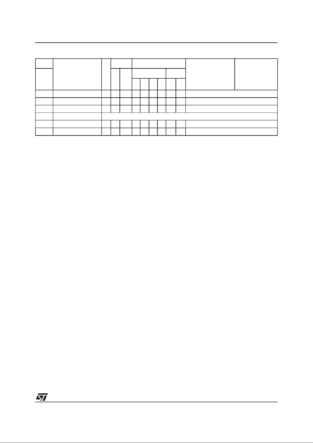
1.3 REGISTER & MEMORY MAP
As shown in Figure 3, the MCU is capable of
adressing 64K bytes of memories and I/O registers.
The available memory locations consist of 64
bytes of register locations, up to 256 bytes of
RAM, 16 bytes of LCD RAM and 4Kbytes of user
program memory. The RAM space includes up to
64 bytes for the stack from 0100h to 013Fh.
The highest address bytes contain the user reset
and interrupt vectors.
Figure 3. Memory Map
0000h
RAM
Program Memory
(4K = 4096 Bytes)
Interrupt & Reset Vectors
HW Registers
014Fh
0040h
003Fh
0150h
EFFFh
Reserved
(see Table 2)
F000h
FFDFh
FFE0h
FFFFh
(see Table 4)
0140h
LCD RAM (16 Bytes)
013Fh
Short Addressing
RAM (zero page)
Stack
(64 Bytes)
0100h
013Fh
0040h
00FFh
(256 Bytes)
Page 9
ST72411R
9/71
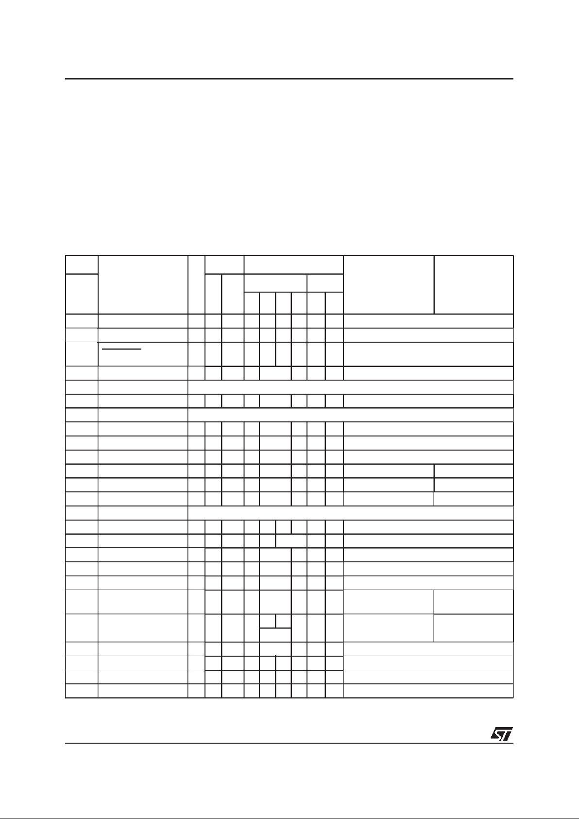
Table 2. Hardware Register Map
Address Block
Register
Label
Register Name
Reset
Status
Remarks
0000h
0001h
0002h
Port A
PADR
PADDR
PAOR
Port A Data Register
Port A Data Direction Register
Port A Option Register
00h
00h
00h
R/W
R/W
R/W
0003h Reserved Area (1 Byte)
0004h
0005h
0006h
Port B
PBDR
PBDDR
PBOR
Port B Data Register
Port B Data Direction Register
Port B Option Register
00h
00h
00h
R/W
R/W
R/W
0007h
to
001Fh
Reserved Area (25 Bytes)
0020h MISCR Miscellaneous Register x0h R/W
0021h
0022h
0023h
Reserved Area (3 Bytes)
0024h LCD LCDCR LCD Control Register 00h R/W
0025h SSS SSSCR
Smartcard Supply Supervisor Control Status
Register
00h R/W
0026h
to
0030h
Reserved Area (11 Bytes)
0031h
0032h
0033h
TIMER
PSCR
TCR
TSCR
Timer Prescaler register
Timer Counter Register
Timer Status Register
FFh
FFh
50h
Read Only
R/W
R/W
0034h
to
003Fh
Reserved Area (12 Bytes)
Page 10
ST72411R
10/71
1.4 FLASH PROGRAM MEMORY
1.4.1 Introduction
Flash devices have a single voltage non-volatile
FLASH memory that may be programmed in-situ
(or plugged in a programming tool) on a byte-bybyte basis.
1.4.2 Main features
■ Remote In-Situ Programming (ISP) mode
■ Up to 16 bytes programmedin the same cycle
■ MTP memory (Multiple Time Programmable)
■ Read-out memory protection against piracy
1.4.3 Structural organisation
The FLASH program memory is organised in a
single 8-bit wide memory block which can be used
for storing both code and data constants.
The FLASH program memory is mappedin the upper part of the ST7 addressing space (F000hFFFFh) and includes the reset and interrupt user
vector area.
1.4.4 In-Situ Programming (ISP) modes
The FLASH program memory canbe programmed
using two Remote ISP modes. These ISP modes
allow the contents of the ST7 program memory to
be updated using a standard ST7 programming
tool after the device is mounted on the application
board. This feature can be implemented with a
minimum numberof addedcomponents and board
area impact.
Examples of Remote ISP hardware interfaces to
the standard ST7 programming tool are described
below. For more details on ISP programming,refer
to the ST7 Programming Specification.
Remote ISP Overview
The Remote ISP modes are initiated by a specific
sequence on the dedicated ISPSEL pin.
The Remote ISP is performedin three steps:
– Selection of the RAM execution mode
– Download of Remote ISP code in RAM
– Execution ofRemote ISP code in RAM to pro-
gram the user program into the FLASH
Remote ISP hardware configuration
Remote ISP mode works using either the internal
oscillator (no external clock is necessary), or an
external square wave clock. The selection of the
oscillator (internal or external) depends on the
ISP_SEL pin during the rising edge of RESET pin
(see “MAIN CLOCK CONTROLLER SYSTEM
(MCC)” on page 21).
Two ISP modes exist:
■ ISP1: ISP signals mapped onsmartcard I/O pins
■ ISP2: ISP signal mapped on general purpose
I/O pins
ISP1 Mode
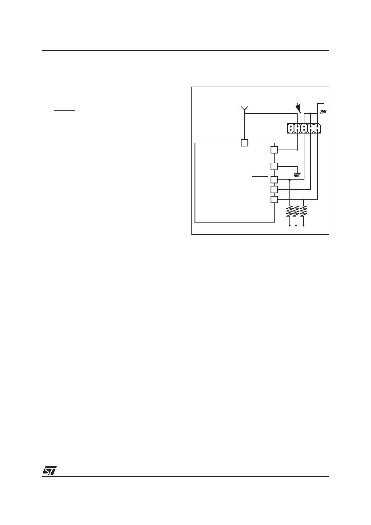
In ISP1 mode, it is possible to re-program the microcontroller using a ISO7816 smartcard connector as shown in Figure 3.
This mode requires five signals (plus the SC_PWR
signal if necessary) to be connected to the programming tool. These signals are:
– RESET: device reset
–VSS: device ground power supply
– ISPCLK1: ISP output serial clock pin
– ISPDATA1: ISP input serial data pin
– ISPSEL: Remote ISP modeselection. Thispin
has an internal pulldown and mustbe left high
impedance if the internal oscillator is selected.
Otherwise an appropriate pull-up is needed
(see Electrical Characteristics).
Note: The RESET and ISPSEL pins are not part of
the ISO7816 interface. Consequently, two additional contacts on the smartcard connector are
necessary.
Table 3. ISP1 (Smartcard) interface
ISPSEL
V
SS
RESET
ISPCLK1
ISPDATA1
ST72411
SMARTCARD
FOR ISP
SMARTCARD
CONNECTOR
SC_PWR
V
DD
ISO7816
Page 11
ST72411R
11/71
FLASH PROGRAM MEMORY (Cont’d)
ISP2 Mode
This mode requires five signals (plus the VDDsignal if necessary) to be connected to the programming tool. These signals are:
– RESET: device reset
–VSS: device groundpower supply
– ISPCLK2: ISP output serial clock pin
– ISPDATA2: ISP input serial data pin
– ISPSEL: Remote ISP mode selection. Thispin
must be left high impedance (internal pull
down on pin ISPSEL) if the internal oscillator
is selected. Otherwise an appropriate pull-up
is needed (see Electrical Characteristics).
If anyof these pins are used for other purposes on
the application, a serial resistor has to be implemented toavoid a conflict if the otherdevice forces
the signal level.
Figure 4 shows a typical hardware interface to a
standard ST7 programming tool. For more details
on the pin locations, refer to the device pinout description.
Figure 4. Typical Remote ISP2 Interface
1.5 Program Memory Read-out Protection
The read-out protection is enabled through an option bit.
For FLASH devices, when this option is selected,
the program and data stored in the FLASH memory are protected against read-out piracy (including
a re-write protection). When this protection option
is removed the entire FLASH program memory is
automatically erased.
ISPSEL
V
SS
RESET
ISPCLK2
ISPDATA2
V
DD
ST7
HE10 CONNECTOR TYPE
TO PROGRAMMING TOOL
APPLICATION
4.7kΩ
1
Page 12
ST72411R
12/71
2 CENTRAL PROCESSING UNIT
2.1 INTRODUCTION
This CPU has a full 8-bit architecture and contains
six internal registers allowing efficient 8-bit data
manipulation.
2.2 MAIN FEATURES
■ 63 basic instructions
■ Fast 8-bit by 8-bit multiply
■ 17 main addressing modes
■ Two 8-bit index registers
■ 16-bit stack pointer
■ Low power modes
■ Maskable hardware interrupts
■ Non-maskable software interrupt
2.3 CPU REGISTERS
The 6 CPU registers shown in Figure 13 are not
present in the memory mapping andare accessed
by specific instructions.
Accumulator (A)
The Accumulator is an 8-bit general purpose register used to hold operands and the results of the
arithmetic and logic calculations and to manipulate
data.
Index Registers (X and Y)
In indexed addressing modes, these 8-bit registers
are used to create either effective addresses or
temporary storage areas for data manipulation.
(The Cross-Assembler generates a precede instruction (PRE) to indicate that the following instruction refers to the Y register.)
The Y registeris not affected by the interrupt automatic procedures (notpushed to and popped from
the stack).
Program Counter (PC)
The program counter is a 16-bit register containing
the address of the next instruction to be executed
by the CPU. It is made of two 8-bit registers PCL
(Program Counter Low which is the LSB) and PCH
(Program CounterHigh which is the MSB).
Figure 5. CPU Registers
ACCUMULATOR
X INDEX REGISTER
Y INDEX REGISTER
STACK POINTER
CONDITION CODE REGISTER
PROGRAM COUNTER
70
1C11HI NZ
RESET VALUE = RESET VECTOR @ FFFEh-FFFFh
70
70
70
0
7
15 8
PCH
PCL
15
87 0
RESET VALUE = STACKHIGHER ADDRESS
RESET VALUE =
1X11X1XX
RESET VALUE = XXh
RESET VALUE = XXh
RESET VALUE = XXh
X = Undefined Value
Page 13

ST72411R
13/71
CPU REGISTERS (Cont’d)
CONDITION CODE REGISTER (CC)
Read/Write
Reset Value: 111x1xxx
The 8-bit Condition Code register contains the interrupt mask and four flags representative of the
result ofthe instruction just executed. Thisregister
can also be handled by the PUSH and POP instructions.
These bits can be individually tested and/or controlled by specific instructions.
Bit 4 = H
Half carry
.
This bit is set by hardware whena carry occurs between bits 3 and 4 of the ALU during an ADD or
ADC instruction. It is reset by hardware during the
same instructions.
0: No half carry has occurred.
1: A half carry has occurred.
This bit is tested using the JRH or JRNH instruction. The H bit is useful in BCD arithmetic subroutines.
Bit 3 = I
Interrupt mask
.
This bit is set by hardware when entering in interrupt or by software to disable all interrupts except
the TRAP software interrupt. This bit is cleared by
software.
0: Interrupts are enabled.
1: Interrupts are disabled.
This bit is controlledby the RIM, SIM and IRET instructions and is tested by the JRM and JRNM instructions.
Note: Interrupts requested while I is set are
latched and can be processed when I is cleared.
By default an interrupt routine is not interruptable
because the I bit is set by hardware when you en-
ter it and reset by the IRET instruction at the end of
the interrupt routine. If the I bit is cleared by software in the interrupt routine, pending interrupts are
serviced regardless of the priority level of the current interrupt routine.
Bit 2 = N
Negative
.
This bit is set and cleared by hardware. It is representative of the result sign of the last arithmetic,
logical or data manipulation. It is a copy of the 7
th
bit of the result.
0:Theresultof the lastoperationis positive or null.
1: The result of the last operation is negative
(i.e. the most significant bit is a logic 1).
This bit isaccessed by the JRMI andJRPL instructions.
Bit 1 = Z
Zero
.
This bit is set and cleared by hardware. This bit indicates thatthe result of the last arithmetic, logical
or data manipulation is zero.
0: The result of the last operation is different from
zero.
1: The result of the last operation is zero.
This bit is accessed by the JREQ and JRNE test
instructions.
Bit 0 = C
Carry/borrow.
This bit is set and cleared by hardware and software. It indicates an overflow or an underflow has
occurred during the last arithmetic operation.
0: No overflow or underflow has occurred.
1: An overflow or underflow hasoccurred.
This bit is driven by the SCF and RCF instructions
and tested by the JRC and JRNC instructions. It is
also affected by the “bit test and branch”, shift and
rotate instructions.
70
111HINZC
Page 14
ST72411R
14/71
CENTRAL PROCESSING UNIT (Cont’d)
STACK POINTER (SP)
Read/Write
Reset Value: 013Fh
The Stack Pointer is a 16-bit register which is always pointingto the next free location in the stack.
It isthen decremented after data has been pushed
onto the stack and incremented before data is
popped from the stack (see Figure 6).
Since the stack is 64 bytes deep, the 10 most significant bits are forced by hardware. Following an
MCU Reset, orafter a Reset Stack Pointer instruction (RSP),the Stack Pointer contains its resetvalue (the SP5 to SP0 bitsare set) whichis the stack
higher address.
The least significant byte of the Stack Pointer
(called S) can be directly accessed by a LD instruction.
Note: When the lower limit is exceeded, the Stack
Pointer wraps around to the stackupper limit, without indicating the stack overflow. The previously
stored information is then overwritten and therefore lost. The stack also wrapsin caseof anunderflow.
The stack is used to save the return address during a subroutine call and the CPU context during
an interrupt. The user may also directly manipulate
the stack by meansof the PUSH and POP instructions. In the case of an interrupt, the PCL is stored
at the first location pointed to by the SP. Then the
other registers are stored in the next locations as
shown in Figure 6.
– When an interrupt is received, the SP is decre-
mented and the context is pushed on the stack.
– On return from interrupt, the SP is incremented
and the context is popped from thestack.
A subroutine call occupies twolocations and an interrupt five locations in the stack area.
Figure 6. Stack Manipulation Example
15 8
00000001
70
0 0 SP5 SP4 SP3 SP2 SP1 SP0
PCH
PCL
SP
PCH
PCL
SP
PCL
PCH
X
A
CC
PCH
PCL
SP
PCL
PCH
X
A
CC
PCH
PCL
SP
PCL
PCH
X
A
CC
PCH
PCL
SP
SP
Y
CALL
Subroutine
Interrupt
Event
PUSH Y POP Y IRET
RET
or RSP
@ 013Fh
@ 0100h
Stack Higher Address = 013Fh
Stack Lower Address =
0100h
Page 15

ST72411R
15/71
3 SUPPLY, RESET AND CLOCK MANAGEMENT
The ST72411 microcontroller includes a range of
utility features for securing the application in critical situations (for example in case of a power
brown-out), and reducing the number of external
components.
Main Features
■ V
DD
Low Voltage Detection and Supervisor
(LVDS)
■ Reset Sequence Manager
■ Main Clock Controller System (MCC)
3.1 LOW VOLTAGE DETECTOR AND
SUPERVISOR (LVDS)
The LVDS consists of three main blocks:
– Low Voltage Detector (LVD)
– Open Power Supply Detection (OPSD)
– Power Supply Supervisor (PSS)
If the internal oscillator is selected (OSC_SEL pin
is tied to VSS), the LVDS, OPSD and PSS functions are always enabled.
If an external clock is selected (OSC_SEL tied to
VDD), the LVDS, OPSD and PSS are disabled
while the external RESET is low and during the
first 260 clock cycles (f
CPU
). They become enabled after this period. Refer to Figure 13. This
means an external reset circuit must be provided.
However, afterthis periodthe LVDS may generate
a reset if a power voltage drop occurs.
3.1.1 Low Voltage Detector
To allow the integration of power management
features in the application, the Low Voltage Detector function (LVD) generates a static reset when
the VDDsupply voltage is below a V
IT+
reference
value (positive-going input thresholdvoltage). This
means that it secures the power-up as well as the
power-down by keeping the ST7 in reset state.
The V
IT-
reference value (negative-going input
threshold voltage) for a voltage drop is lower than
the V
IT+
reference value for power-on in order to
avoid a parasitic reset when the MCU starts running and sinks current on the supply(hysteresis).
The LVD Reset circuitry generates a reset when
VDDis below:
–V
IT+
when VDDis rising
–V
IT-
when VDDis falling
The LVD function is illustrated in Figure 7.
Provided the minimum VDDvalue (guaranteed for
the oscillator frequency) is below V
IT-
, the MCU
can only be in one of two modes:
– Under full software control
– In static safe reset
In this condition, secure operation is always ensured for the application without the need for external reset hardware.
The LVD filters spikes on VDDlarger than t
g(VDD)
to
avoid parasitic resets.
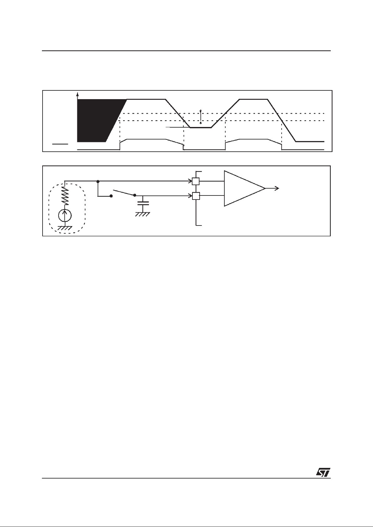
3.1.2 Open Power Supply Detection (OPSD)
The purpose of the Open Power Supply Detection
function is to detect if the VDDpower circuit is
open.
It detects if the microcontroller is about to be powered down, to allow software to shutdown the application properly before the Power Down Reset
generate by the LVDS.
The system is based on a comparison between
V
REF
andVDD.V
REF
is an analog input which is intended to be directly connected to the power
source (see Figure 8).
The detection is not dependent on the MCU consumption (not dependent on the voltage drop due
to the internal resistor of the power source).
To avoid spurious setting of the Power Down Flag
due to possible noise (PDF bit in the MISCR register), a margin M is factored into the comparison.
The detectionis done if:
(V
REF-VDD
)>M
The PDF flag can be used to monitor the main
supply supervisor function as shown in Figure 9.
When (V
REF-VDD
) > M, the PDFflag is set and an
interrupt is generated if the PDIE bit in the MISCR
register is set. This feature allows the user program to detect and manage the VDDdrop according to the application before the reset generated
by the LVDS (See Figure 9).
See the Miscellaneous register chapter for more
details on the PDF and PDIE bits.
3.1.3 Power Supply Supervisor (PSS)
The Power Supply Supervisor function compares
the Power Supply to a fixed analog reference voltage (V
PSS
) (see Figure 10). The output of this
comparator is directly connected to the PSSF bitin
the MISCR register (read only bit).
This feature can be used to monitor the power
supply.
Page 16
ST72411R
16/71
LOW VOLTAGE DETECTOR AND SUPERVISOR (Cont’d)
Figure 7. Low Voltage Detector vs Reset
Figure 8. Open Power Supply Detection: V
REF
Connections
V
DD
V
IT+
RESET
V
IT-
HYSTERESIS
V
hys
V
DD
V
REF
R
S
Power
V
E
+
-
C
Power Down Flag
Source
(PDF)generation
SW1
if (V
REF-VDD
)>M
Page 17
ST72411R
17/71
LOW VOLTAGE DETECTOR AND SUPERVISOR (Cont’d)
Figure 9. Open Power Supply Detection (OPSD)
Figure 10. Power Supply Supervisor system (PSS)
V
’’
RESET
V
IT+
V
IT-
HYSTERESIS
V
hys
PDF
Internal RESET
RUN
Open V
DD
detection
V
5()
V
5()
V
’’
DV = RS.I
RUN
V
E
V
DDRUN
V
DDRUN
0V
+V
E
RESET
SW1 OPEN SW1 CLOSED SW1 OPEN
0V
0V
V
5( )
V
’’
M
(CAPACITOR
DISCHARGED)
Page 18
ST72411R
18/71
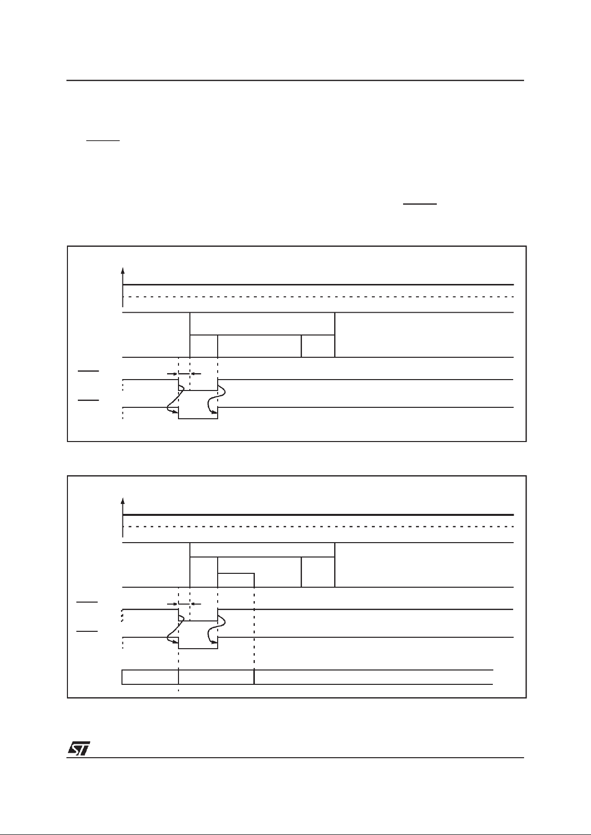
3.2 RESET SEQUENCE MANAGER
The RESET sequence manager includes two reset sources as shown in Figure 11:
■ External RESET source pulse
■ Internal LVDS RESET (Low Voltage Detection)
These sources act on the RESET PIN and it is always kept low during the delay phase.
The RESET service routine vector is fixed at addresses FFFEh-FFFFh in the ST7 memory map.
A 4096 CPUclock cycle delay allows the oscillator
to stabilise and to ensure that recovery has taken
place from the Reset state.
The RESET vector fetch phase duration is 2 clock
cycles.
Figure 11. Reset Block Diagram
f
CPU
COUNTER
RESET
R
ON
V
DD
LVD RESET
INTERNAL
RESET
Page 19
ST72411R
19/71
RESET MANAGER (Cont’d)
([WHUQD O 5(6( 7 SLQ
The RESETpin is both an input andan open-drain
output with integrated RONweak pull-up resistor
(see Figure11). This pull-up has nofixed value but
varies in accordance with the input voltage. It can
be pulled low by external circuitry to reset the device.
A RESET signal coming from an external source
must have a duration of at least t
PULSE
in order to
be recognized. Two RESET sequences can be associated with this RESET source as shown in Figure 12.
When the RESET is generated by an internal
source, during the two first phases of the RESET
sequence, the device RESET pin acts as an output that is pulled low.
Figure 12. External RESET Sequence with internal Clock Selected (OSC_SEL pin tied to VSS)
Figure 13. External RESET Sequence with External Clock Selected (OSC_SEL pin tied to VDD)
5(6(7
581
INTERNAL RESET
4096 CLOCK CYCLES
FETCH
VECTOR
581
t
PULSE
9
’’
V
IT+
V
DD nominal
DELAY
RESET PIN
EXTERNAL
RESET SOURCE
5(6(7
581
INTERNAL RESET
260 CLOCK
FETCH
VECTOR
581
t
PULSE
9
’’
V
IT+
V
DD nominal
DELAY
LVDS,
ONOFF
OPSD,
PSS
4096 CLOCK CYCLES
CYCLES
ON
RESET PIN
EXTERNAL
RESET SOURCE
Page 20
ST72411R
20/71
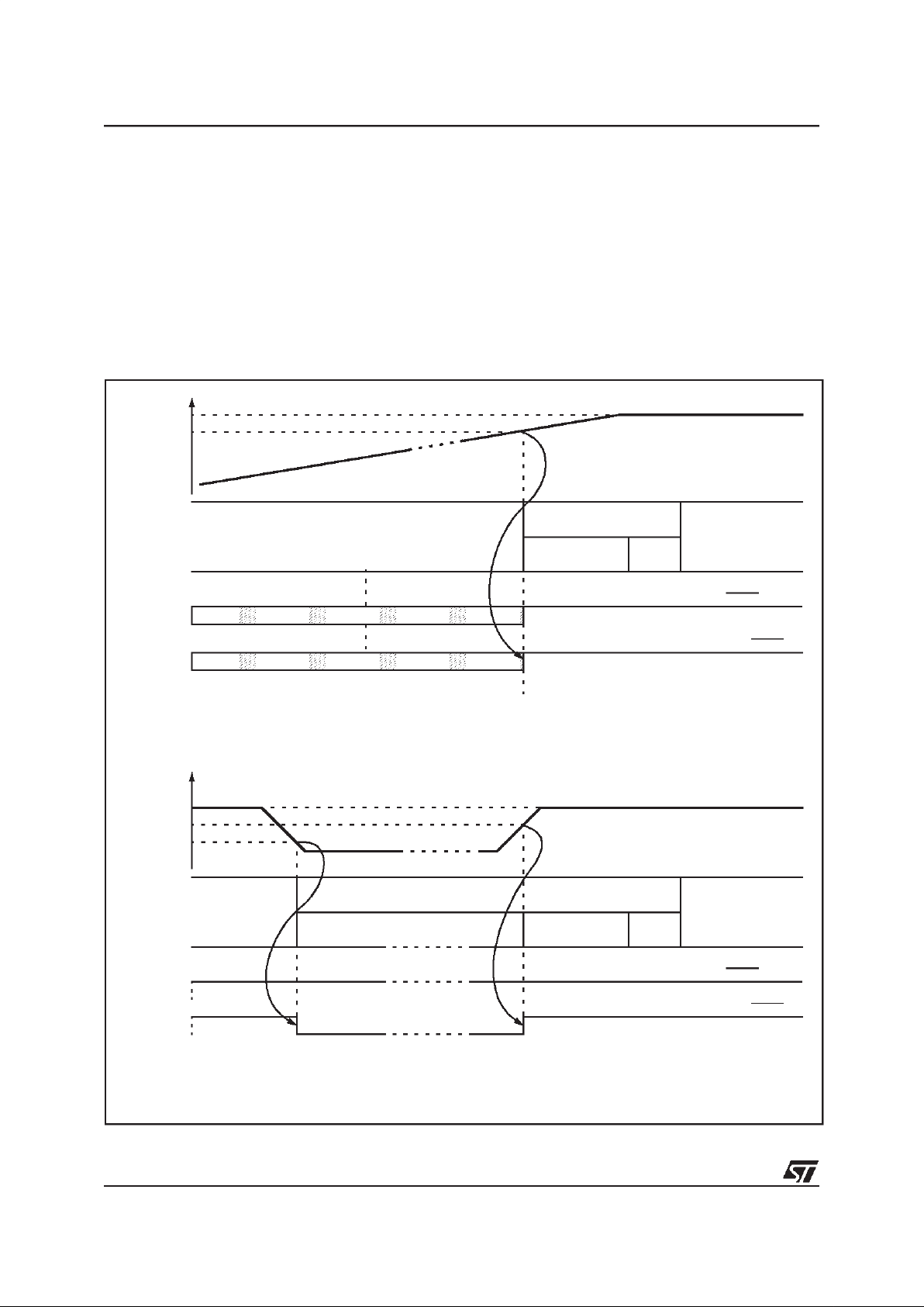
RESET MANAGER (Cont’d)
,QWHUQD O /RZ 9ROWDJ H ’HWHFWL RQ 5 ( 6 ( 7
Two different RESET sequences caused bythe internal LVD circuitry can be distinguished:
- LVD Power-On RESET
- Voltage Drop RESET
In the second sequence, a “delay” phase is used
to keep the device in RESET state until VDDrises
up to V
IT+
(see Figure 14).
Important: if OSC_SEL pin is HIGH (external
clock selected), the LVD Power-On and the Voltage Drop featuresare disabled during the first 260
clock cycles (f
CPU
) after reset. This means that an
external reset circuitry must be provided to reset
the microcontroller.
Figure 14. LVD RESET Sequences when the OSC_SEL pin is tied to GND
5( 6( 7
581
INTERNAL RESET
4096 CLOCK CYCLES
FETCH
VECTOR
32 : ( 5
RESET PIN
EXTERNAL RESET SOURCE
5(6(7
581
INTERNAL RESET
4096 CLOCK CYCLES
FETCH
VECTOR
581
RESET PIN
EXTERNAL RESET SOURCE
9
’’
V
DDnominal
DELAY
V
IT+
V
IT-
9
’’
V
DDnominal
V
IT+
/
9
’
3
2
:
(
5
2
1
5
(
6
(
7
9
2
/
7
$
*
(
’
5
2
3
5
(
6
(
7
2))
7KH 2 6 &B6( / SLQ LV WLHG WR 9
66
LQWHU QD O FORFN VHOHFWHG / 9 ’ 6 D OZD\V DFWLYDWHG
7KH 2 6&B6( / SLQ LV WLHG WR * 1 ’
LQWHU QDO FORFN
V
HOHFWHG / 9 ’ 6 DOZD\V DFWLYDWHG
Page 21
ST72411R
21/71
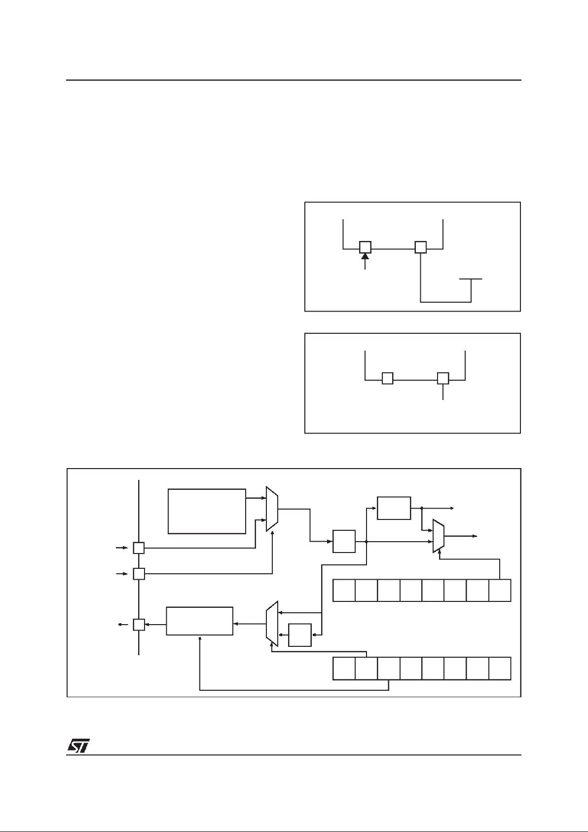
3.3 MAIN CLOCK CONTROLLER SYSTEM (MCC)
The MCC block supplies the clock for the ST7
CPU and its internal peripherals. It allows to manage the SLOW power saving mode acting on the
SMS bit of the Miscellaneous register (MISCR)
and the Main clock-out capability acting on the
CKD and CKAFOEN bits of the Smartcard Supply
Supervisor ControlRegister (SSSCR).
The main clock of the ST7 can be generated by
two different sources (see Figure 17):
■ an external source
■ an internal RC oscillator
The device is normally operated using anintegrated 7.16MHz oscillator, meaning 3.58MHz operating frequency. However, an external clock can be
applied, up to 8MHz (4MHz operating frequency).
The clock source is selected through the
OSC_SEL pin status.
([WHUQD O &ORFN 6RXUFH
The OSC_SEL pin status selects the External
Clock capability when it is tied to VDD. In this
mode, a clock signal with ~50% duty cycle has to
drive the OSCIN pin (see Figure 15).
,QWHUQD O 5& 2VFLOODWRU 6RXUFH
The OSC_SEL pin status selects the Internal RC
clock source capability when it is tied to VSS(see
Figure 16).
Note that OSC_SEL pin contains a pull-down
which allows to leave OSC_SEL in high impedance in the applicationwhen the internal oscillator
is selected. This is mandatory for using the Remote In Situ Programming feature.
Figure 15. External Clock
Figure 16. Internal RC Oscillator
Figure 17. Main Clock Controller (MCC) Block Diagram
OSCIN OSC_SEL
EXTERNAL
ST7
SOURCE
V
DD
OSCIN OSC_SEL
ST7
highZ
(internal pulldown is present)
DIV 2
SMS--
MISCR
f
OSC
f
CPU
OSCIN
-----
INTERNAL
RC OSCILLATOR
7.16 MHz
OSC_SEL
DIV 16
SMARTCARD
interface
LCD and TIMER
---
SSSR
CK_A
--CKD-
FOEN
DIV 2
I/O ALTERNATE
FUNCTION
SC_CK
Page 22

ST72411R
22/71
4 INTERRUPTS
The ST7 core may be interruptedby one of two different methods: maskable hardware interrupts as
listed in the Interrupt Mapping Table and a nonmaskable software interrupt (TRAP). The Interrupt
processing flowchart is shown in Figure 1.
The maskableinterrupts must be enabled clearing
the I bit in order to be serviced. However, disabled
interrupts may be latched and processed when
they are enabled (see external interrupts subsection).
When an interrupt has to be serviced:
– Normal processing is suspended at the end of
the current instruction execution.
– The PC, X, A and CC registers are saved onto
the stack.
– The I bit of the CC register is set to prevent addi-
tional interrupts.
– ThePC is then loaded withtheinterrupt vector of
the interruptto service and the first instruction of
the interrupt service routine is fetched (refer to
the Interrupt Mapping Table for vector addresses).
The interrupt service routine should finish with the
IRET instruction which causes the contents of the
saved registers to be recovered from thestack.
Note: As a consequence of the IRET instruction,
the I bit will be cleared and the main program will
resume.
Priority management
By default, a servicing interrupt cannot be interrupted because the I bit is set by hardware entering in interrupt routine.
In the case when several interrupts are simultaneously pending, an hardware priority defines which
one will be serviced first (see the Interrupt Mapping Table).
Interrupts and Low power mode
All interrupts allow the processor to leave the
WAIT low power mode. Only external and specifically mentioned interrupts allow the processor to
leave the HALT low power mode (refer to the “Exit
from HALT“ column in the Interrupt Mapping Table).
4.1 NON MASKABLE SOFTWARE INTERRUPT
This interrupt is entered when the TRAP instruction is executed regardless of the state of the I bit.
It will be serviced according to the flowchart on
Figure 1.
4.2 EXTERNAL INTERRUPTS
External interrupt vectors can be loaded into the
PC register if the corresponding external interrupt
occurred and if the I bit is cleared.These interrupts
allow the processor to leave the Halt low power
mode.
The external interrupt polarity is selected through
the miscellaneous register or interrupt register (if
available).
An external interrupt triggered on edge will be
latched and the interrupt request automatically
cleared upon entering the interrupt serviceroutine.
If several input pins, connected to the same interrupt vector, are configured as interrupts, their signals are logically ANDed before entering the edge/
level detection block.
Caution:The type of sensitivity defined inthe Miscellaneous or Interrupt register (if available) applies to the ei source. In case of an ANDedsource
(as described on the I/O ports section), a lowlevel
on an I/O pin configured as input with interrupt,
masks the interrupt requesteven in case of risingedge sensitivity.
4.3 PERIPHERAL INTERRUPTS
Different peripheral interrupt flags in the status
register are able to cause an interrupt when they
are active if both:
– The I bit of the CC register is cleared.
– Thecorrespondingenablebit isset in the control
register.
If any of these two conditions is false, the interrupt
is latched and thus remains pending.
Clearing an interrupt request is done by:
– Writing “0”to the corresponding bit in the status
register or
– Access tothe status registerwhile the flag is set
followed by a read or write of an associated register.
Note: the clearing sequence resets the internal
latch. A pending interrupt (i.e. waiting for being enabled) will therefore be lost ifthe clear sequence is
executed.
Page 23

ST72411R
23/71
INTERRUPTS (Cont’d)
Figure 18. Interrupt Processing Flowchart
I BIT SET?
Y
N
IRET?
Y
N
FROM RESET
LOAD PC FROM INTERRUPT VECTOR
STACK PC, X, A, CC
SET I BIT
FETCH NEXT INSTRUCTION
EXECUTE INSTRUCTION
THIS CLEARS I BIT BY DEFAULT
RESTORE PC, X, A, CC FROM STACK
INTERRUPT
Y
N
PENDING?
Page 24

ST72411R
24/71
INTERRUPTS (Cont’d)
Table 4. Interrupt Mapping
N°
Source
Block
Description
Register
Label
Priority
Order
Exit
from
HALT
Address
Vector
RESET Reset
N/A
Highest
Priority
Lowest
Priority
yes FFFEh-FFFFh
TRAP Software Interrupt no FFFCh-FFFDh
0 Not used
-
FFFAh-FFFBh
1 Not used FFF8h-FFF9h
2 EI0 External Interrupt Port A7..0
N/A yes
FFF6h-FFF7h
3 EI1 External Interrupt Port B6..0 FFF4h-FFF5h
4 Not used
-
FFF2h-FFF3h
5 Not used FFF0h-FFF1h
6 Not used FFEEh-FFEFh
7 Not used FFECh-FFEDh
8 TIMER Timer Underflow Interrupt TSCR yes FFEAh-FFEBh
9 Not used FFE8h-FFE9h
10 Not used FFE6h-FFE7h
11 Not used FFE4h-FFE5h
12 SSS Smartcard Current Overload Interrupt SSSR no FFE2h-FFE3h
13 LVDS Power Down Interrupt MISCR no FFE0h-FFE1h
Page 25

ST72411R
25/71
4.4 POWER SAVING MODES
4.4.1 Introduction
There are three Power Saving modes. Slow Mode
is selected by setting the relevant bits in the Miscellaneous register. Wait and Halt modes may be
entered using the WFI and HALT instructions.
Table 5. Power Saving Modes
1
Except with external timer clock.
2
If the LVD bit in the MISCR register is reset
Note: To reduce power consumption (in Run or
Wait modes), the smartcard supply supervisor
(SSS) and the LCD can be disabled by software.
4.4.2 Slow Mode
In Slow mode, the oscillator frequency can be divided by a value defined in the Miscellaneous
Register. The CPU and peripherals are clocked at
this lower frequency except theLCD driver and the
8-bit Timerwhich have a fixed clock. Slow modeis
used to reduce power consumption, and enables
the user to adapt the clock frequency to the available supply voltage.
4.4.3 Wait Mode
Wait mode places the MCU in a low power consumption mode by stopping the CPU. The peripherals remain active. During Wait mode, the I bit
(CC Register) is cleared, so as to enable all interrupts. All other registers and memory remain unchanged. The MCU will remain in Wait mode until
an Interruptor Resetoccurs, the Program Counter
then branches to the starting address of the Interrupt or Reset Service Routine.
The MCUwill remainin Wait mode until aReset or
an Interrupt occurs, causing it to wake up.
Refer to Figure 19.
Figure 19. Wait Mode Flow Chart
Mode f
CPU
CPU
Peripherals
switched off.
Wake up
Slow f
OSC
/32 ON None -
Wait
f
OSC
/2
or
f
OSC
/32
OFF None
- External I/O
- Timer
- LVDS (PDF Flag).
- Reset
Halt OFF OFF
- SSS
- TIMER
1
- LVDS
2
- LCD
- External I/O
- Timer
- Reset
WFI INSTRUCTION
RESET
INTERRUPT
Y
N
N
Y
CPU CLOCK
OSCILLATOR
PERIPH. CLOCK
I-BIT
ON
ON
CLEARED
OFF
CPU CLOCK
OSCILLATOR
PERIPH. CLOCK
I-BIT
ON
ON
SET
ON
FETCH RESET VECTOR
OR SERVICE INTERRUPT
4096 CPU CLOCK
CYCLES DELAY
IF RESET
Note: Before servicing an interrupt, the CC register is
pushed on the stack. The I-Bit is set during the interrupt routine and cleared when the CC register is
popped.
Page 26

ST72411R
26/71
POWER SAVING MODES (Cont’d)
4.4.4 Halt Mode
The Halt mode is the lowest power consumption
mode of the MCU. Halt modeis entered byexecuting the HALT instruction. The internal oscillator is
then turned off, causing all internal processing to
be stopped, including the operation of the on-chip
peripherals.
When entering Halt mode, the I bit in the CC Register is cleared so as to enable External Interrupts.
If an interrupt occurs, the CPU becomes active.
The MCU can exit Halt modeon reception of an interrupt or a reset. Refer to the Interrupt Mapping
Table. The oscillator is then turned onand a stabilization time is provided before releasing CPU operation. The stabilization time is 4096 CPU clock
cycles.
After the start up delay, the CPU continues operation by servicing the interrupt which wakes it up
or by fetching the reset vector if a reset wakes it
up.
Note: If the LVD bit in the MISCR register is set,
the LVDS is not disabled when entering Halt
mode.
Figure 20. HALT Flow Chart
N
N
EXTERNAL
INTERRUPT*
RESET
HALT INSTRUCTION
4096 CPU CLOCK
FETCH RESET VECTOR
OR SERVICE INTERRUPT
CYCLES DELAY
CPU CLOCK
OSCILLATOR
PERIPH. CLOCK
I-BIT
ON
ON
SET
ON
CPU CLOCK
OSCILLATOR
PERIPH. CLOCK
I-BIT
OFF
OFF
CLEARED
OFF
Y
Y
* or some specific interrupts
Note: Before servicing an interrupt, the CC register is
pushed on the stack. The I-Bit is set during the interrupt routine and cleared when the CC register is
popped.
Page 27

ST72411R
27/71
5 ON-CHIP PERIPHERALS
5.1 I/O PORTS
5.1.1 Introduction
The I/O ports offer different functional modes:
– transferof data through digitalinputs and outputs
and for specific pins:
– external interrupt generation
– alternate signal input/output for the on-chip pe-
ripherals.
An I/O port contains up to 8 pins. Each pin can be
programmed independently as digital input (with or
without interrupt generation)or digital output.
5.1.2 Functional Description
Each port is associated to 2 main registers:
– Data Register (DR)
– Data Direction Register (DDR)
and one optional register:
– Option Register (OR)
Each I/Opin may beprogrammed using the corre-
sponding registerbits in DDR and ORregisters: bit
X corresponding to pinX of the port. The samecorrespondence is used for the DR register.
The following description takes into account the
OR register, for specific port which do not provide
this register refer to the I/O Port Implementation
section. The generic I/O block diagram is shown
on Figure 21.
Input Modes
The input configuration is selected by clearing the
corresponding DDR register bit.
In this case, reading the DR register returns the
digital value applied to the external I/O pin.
Different input modes can beselected by software
through the OR register.
Note1: Writing the DR register modifies the latch
value but does not affect the pin status.
Note2: When switching from input to output mode,
the DR register has to be written first to drive the
correct levelon the pinas soon as the ports is configured as an output.
External interrupt function
When an I/O is configured in Input with Interrupt,
an event on this I/O can generate an external Interrupt request to the CPU.
Each pin can independently generate an Interrupt
request. The interrupt sensitivity is given independently according to the description mentioned
in the Miscellaneous register.
Each external interrupt vector is linked to a dedicated group of I/O port pins (see Interrupt section).
If more than one input pins are selected simultaneously as interrupt source, these are logically ANDed. For this reason if one of the interrupt pins is
tied low, it masks the other ones.
In case of a floating input with interrupt configuration, special cares mentioned in the IO port implementation section have to betaken.
Output Mode
The output configuration is selected by setting the
corresponding DDR register bit.
In this case, writing the DR register applies this
digital value to the I/O pin through the latch. Then
reading the DR register returns the previously
stored value.
Two different output modes can be selected by
software through the OR register: Output push-pull
and open-drain.
DR register value and output pin status:
Note: In this mode, interrupt function is disabled.
Alternate function
When an on-chip peripheral is configured to use a
pin, the alternate function is automatically selected. This alternate function takes priority over the
standard I/O programming.
When the signal is coming froman on-chip peripheral, the I/O pin is automatically configured in output mode (push-pull or open drain according to the
peripheral).
When the signal is going to an on-chip peripheral,
the I/O pin has to be configured in input mode. In
this case, the pin’s state is also digitally readable
by addressing the DR register.
Note: Input pull-up configuration can cause unexpected value atthe input of the alternate peripheral
input. Whenan on chip peripheral use a pin as input and output, this pin has to be configured in input floating mode.
WARNING: The alternate function mustnot be activated as long as the pin is configured as input
with interrupt,in order toavoid generating spurious
interrupts.
DR Push-pull Open-drain
0V
SS
Vss
1V
DD
or V
SC_PWR
Floating
Page 28

ST72411R
28/71
I/O PORTS (Cont’d)
Smartcard versus Standard I/Os
The SmartcardI/O ports differfrom thestandard I/
O ports in that they have a different power supply:
the output buffers and the input Schmitt trigger are
supplied by V
SC_PWR
for the Smartcard I/Os and
by VDDfor the Standard I/Os.For Smartcard I/Os,
the Schmitttrigger is designed to guarantee output
levels compatible with VDDfor V
SC_PWR
=5V or
3V.
Caution: When the SSS regulator is deactivated
(bit SSSEN=0), the Smartcard I/O ports cannot be
used correctly (VSC_PWR=VSS). In this case,
special care is required when manipulating external interrupts: As Smartcard I/Os are always tied
to ground, they may mask interrupts on other I/O
lines of the same port.
Figure 21. I/O Block Diagram
Table 6. Port Mode Options
NI - not implemented
Off - implemented not activated
On - implemented and activated
DR
DDR
OR
DATA BUS
PAD
V
DD
or V
SC_PWR
ALTERNATE
ENABLE
ALTERNATE
OUTPUT
1
0
OR SEL
DDR SEL
DR SEL
INTERRUPT
PULL-UP
CONDITION
P-BUFFER
(OPTION*)
N-BUFFER
PULL-UP
(OPTION*)
1
0
* SEE TABLE BELOW
ANALOG
INPUT
If implemented
ALTERNATE
INPUT
V
DD
or V
SC_PWR
DIODES
(OPTION*)
V
DD
or V
SC_PWR
PULL-DOWN
CONDITION
Configuration Mode Pull-Up P-Buffer Diodes
Input
Floating Off
Off
On
Pull-up with Interrupt On
Output
Push-pull
Off
On
Open Drain (logic level) Off
Push-pull with pull-up
On
On
Open Drain (logic level) with pull-up Off
True Open Drain NI
Page 29

ST72411R
29/71
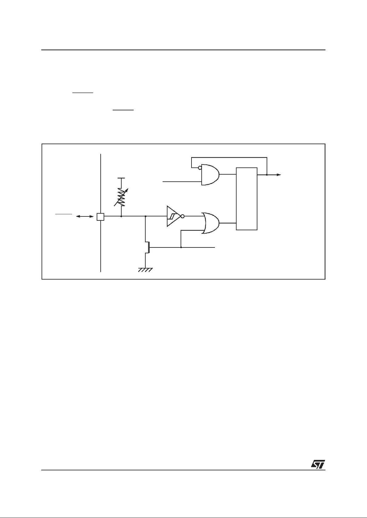
I/O PORTS (Cont’d)
5.1.3 I/O Port Implementation
The I/O port register configurations are summarised as follows.
Standard Ports
PA0:7, PB5 (supplied by VDD)
PB6 (supplied by VDD)
PB0, 2, 3, 4 (supplied by V
SC_PWR
)
PB1 (Smartcard Data supplied by V
SC_PWR
)
Switching these I/O ports from one state to another should be done in a sequence that prevents unwanted side effects. Recommended safe transitions are illustrated in Figure 22 Other transitions
are potentially risky and should be avoided, since
they are likely to present unwanted side-effects
such as spurious interrupt generation.
Figure 22. Interrupt I/O Port State Transition
Table 7. Port Configuration
* Note: Smartcard I/Os supplied by V
SC_PWR
.
MODE DDR OR
floating input 0 0
pull-up input with interrupt 0 1
open drain output 1 0
push-pull output 1 1
MODE DDR OR
floating input 0 0
pull-down input with interrupt 0 1
open drain output 1 0
push-pull output 1 1
MODE DDR OR
floating input 0 0
pull-up input with interrupt 0 1
open drain output 1 0
push-pull output 1 1
MODE DDR OR
pull-up input 0 0
pull-up input with interrupt 0 1
open drain output with pull-up 1 0
push-pull output with pull-up 1 1
01
pull-up
interrupt
INPUT
00
floating
(reset state)
INPUT
10
open-drain
OUTPUT
11
push-pull
OUTPUT
XX
= DDR, OR
Port Pin name
Input Output
OR = 0 OR = 1 OR = 0 OR = 1
Port A PA7:0 floating pull-up interrupt open drain push-pull
Port B
PB6 floating pull-down interrupt open drain push-pull
PB5 floating pull-up interrupt open drain push-pull
PB4:2 (SC*) floating pull-up interrupt open drain push-pull
PB1 (SC*) pull-up pull-up interrupt pull-up open drain pull-up push-pull
PB0 (SC*) floating pull-up interrupt open drain push-pull
Page 30

ST72411R
30/71
I/O PORTS (Cont’d)
5.1.4 Register Description
’ $7$ 5(*,67(5 ’ 5
Port x Data Register
PxDR with x = A or B.
Note: In Port B, PB[7] is unused.
Read/Write
Reset Value: 0000 0000 (00h)
Bit 7:0 = D[7:0]
Data register 8 bits.
The DR register has a specific behaviour according to the selectedinput/output configuration. Writing the DR register is always taken into account
even ifthe pin is configuredas aninput; this allows
to always have the expected level on the pin when
toggling to output mode. Reading the DR register
returns either the DR register latch content (pin
configured asoutput) or the digitalvalue applied to
the I/O pin (pin configured as input).
DATA DIRECTION REGISTER (DDR)
Port x Data Direction Register
PxDDR with x = A or B.
Read/Write
Reset Value: 0000 0000 (00h)
Bit 7:0 = DD[7:0]
Data direction register 8 bits.
The DDR register gives the input/output direction
configuration of the pins. Each bits is set and
cleared by software.
0: Input mode
1: Output mode
237,2 1 5(*,67(5 25
Port x Option Register
PxOR with x = A or B.
Read/Write
Reset Value: 0000 0000 (00h)
Bit 7:0 = OR[7:0]
Option register 8 bits.
For specific I/O pins, this register is not implemented. In this case the DDR register is enough to select the I/O pin configuration.
The OR register allows to distinguish: in input
mode if the pull-up (or pull-down for PB6) with interrupt capability or the floating (pull-up for PB1)
configuration is selected, in output mode if the
push-pull or open drain configuration is selected.
Each bit is set and cleared by software.
70
D7 D6 D5 D4 D3 D2 D1 D0
70
DD7 DD6 DD5 DD4 DD3 DD2 DD1 DD0
70
O7 O6 O5 O4 O3 O2 O1 O0
Page 31

ST72411R
31/71
I/O PORTS (Cont’d)
Table 8. I/O Port Register Map and Reset Values
Address
(Hex.)
Register
Label
76543210
Reset Value
of all IO port registers
00000000
0000h PADR
MSB LSB0001h PADDR
0002h PAOR
0004h PBDR
- MSB LSB0005h PBDDR
0006h PBOR
Page 32

ST72411R
32/71
5.2 MISCELLANEOUS REGISTER
The miscellaneous register allows control over
several features such as the external interrupts or
the I/O alternate functions.
5.2.1 I/O Port Interrupt Sensitivity Description
The external interrupt sensitivity is controlled by
the IPBand IS[1:0]bits ofthe Miscellaneous register (Figure 23). Up to 2 fully independent external
interrupt source sensitivities are allowed.
Each external interrupt source can be triggered by
four different events on the pin:
■ Falling edge
■ Rising edge
■ Falling and rising edge
■ Falling edge and low level
To guarantee the functionality, a modification of
the sensitivity in the MISC register can be done
only when the I bit of the CC register is set to 1 (interrupt masked). See I/O port register and Miscellaneous register descriptions for more details on
programming.
Caution: Take care when changing the value of
the IPB bit as, in some cases, an interrupt will be
generated by the edge resulting from the change.
5.2.2 Slowmode and VDDSupply Monitoring
The MISCRregister manages SLOW mode selection and the LVDSVDDmonitoring interrupt. Refer
to the register description.
Figure 23. External Interrupt Sources vs MISCR
EI1
INTERRUPT
SOURCE
EI0
INTERRUPT
SOURCE
IS0IS1
MISCR
SENSITIVITY
CONTROL
PB6
IPB
PB0
SOURCES
PA7
PA0
SOURCES
Page 33

ST72411R
33/71
MISCELLANEOUS REGISTER (Cont’d)
0,6&(//$1(286 5(*,67(5 0 ,6&5
Read/Write
Reset Value: x000 0000 (x0h)
(for bit 7, the reset value depends on VDD)
Bit 7 = PSSF
Power Supply Supervisor Flag
This bit is set and cleared by hardware.
0: VDDis greater than V
PSS
.
1: VDDis less than V
PSS
.
Bit 6= LVD
LVD ON during HALT mode
This bit is set and cleared by software.
This bit is used to keep the LVD active during
HALT mode.
0: LVD switched off in HALT mode (reset state).
1: LVD active in HALT mode.
Bit 5 = IPB
Interrupt polarity for port B
This bit is used to reverse the external interrupt
sensitivity polarity of the port B[6:0] pins. It is set
and cleared by software.
0: Standard sensitivity polarity
1: Reversed sensitivity polarity
Note: See IS[1:0] bit description for more details.
This bit canbe written onlywhen the I bit of theCC
register is set to 1(if interrupts are masked).
Bit 4:3 = IS[1:0]
EI0 and EI1 sensitivity
These bits are used to program the interrupt sensitivity of the following external interrupts:
- EI1 (port B[6:0])
- EI0 (port A[7:0])
These 2 bits can be written only when the I bit of
the CC register is set to 1 (interrupt masked).
Bit 2 = PDIE
Power Down Interrupt Enable
This bit is set andcleared by software.
0: Power down interrupt disabled
1: Power down interrupt enabled
Bit 1 = PDF
Power Down Flag
This bit is set and cleared by software or set by
hardware if(V
REF-VDD
) > M. If the PDIEbit is set,
an interrupt is generated when PDF is set (sensitivity is high level). It can be cleared only by software writing zero. It can also be set by software,
generating an interrupt if PDIE is enabled.
0: (V
REF-VDD
) < M: No open VDDcircuit detected
1: (V
REF-VDD
) > M : Open VDDcircuit detected.
Bit 0 = SMS
Slow mode select
This bit is set andcleared by software.
0: Normal mode. f
CPU
= f
OSC
/2
1: Slow mode. f
CPU
= f
OSC
/32
See low power mode and MCC chapters for more
details.
76543210
PSSF LVD IPB IS1 IS0 PDIE PDF SMS
IS1 IS0
External Interrupt Sensitivity
MISCR.IPB=0 MISCR.IPB=1
00
Falling edge &
low level
Rising edge
& high level
0 1 Rising edge only Falling edge only
1 0 Falling edge only Rising edge only
1 1 Rising and falling edge
IS1 IS0 External Interrupt Sensitivity
0 0 Falling edge & low level
0 1 Rising edge only
1 0 Falling edge only
1 1 Rising and falling edge
Page 34

ST72411R
34/71
5.3 8-BIT TIMER (TIM8)
5.3.1 Introduction
The 8-Bit Timer on-chip peripheral (TIM8) is a free
running downcounter based on an 8-bit downcounter with a 9-bit programmable prescaler.
5.3.2 Main Features
■ Timeout downcounting mode with up to 16-bit
accuracy
■ External counter clock source (valid also in
HALT mode)
■ Interrupt capability on counter underflow
■ Output signal generation
■ External pulse length measurement
■ Time base interrupt
The timer can be used in WAIT and HALT modes
and to wake upthe MCU.
Figure 24. Timer Block Diagram
f
TIMER
/8
f
TIMER
/64
f
TIMER
/512
UDF INTERRUPT
OEN TOUT DOUT UDF ETI PSE PS1 PS0
TSCR
PROGRAMMABLE PRESCALER
PSCR7 PSCR6 PSCR5 PSCR4 PSCR3 PSCR2 PSCR1 PSCR0
PSCR
0
PSCR8
852
70
TCR7 TCR6 TCR5 TCR4 TCR3 TCR2 TCR1 TCR0
TCR
70
UNDERFLOW
RELOAD
8-BIT COUNTER
ALTERNATE
FUNCTION
TIMIO
f
TIMER
f
TIMER
f
COUNTER
f
EXT
DIV16
DIV2
f
CPU
f
OSC
LATCH
Page 35

ST72411R
35/71
8-BIT TIMER (Cont’d)
5.3.3 Counter/Prescaler Description
Counter
The free running 8-bit downcounter is fed by the
output of the programmable prescaler, and is decremented on every rising edge of the f
COUNTER
clock signal.
It is possible to read or write the contents of the
counter on the fly, by reading or writing the timer
counter register (TCR).
When a counter underflow occurs, the counter is
automatically reloaded with the value FFh.
Counter clock and prescaler
The counter clock frequency is given by:
f
COUNTER=fTIMER
/8
PS[1:0]
where f
TIMER
can be:
–f
CPU
/16
–f
EXT
(input on TIMIO pin)
–f
CPU
/16 gated by TIMIO pin
Table 13 lists the values that f
COUNTER
can take if
f
TIMER
is f
CPU
/16.
Table 9. f
counter
values for a f
cpu
=3.58MHz
The timer input clock (f
TIMER
) feeds the 9-bit programmable prescaler. The prescaler output can be
programmed by selecting one of the 4 available
prescaler taps using the PS[1:0] bits in the Status/
Control Register (TSCR). Thus the division factor
of the prescaler can be set to 8n(where nequals 0,
1, 2 or 3). See Figure 38.
The clock input is enabled by the PSE (Prescaler
Enable) bit in the TSCR register. When PSE is reset, the counter is frozen andthe prescaler is loaded with the value 1FFh. When PSE is set, the
prescaler and thecounter run at the rate of the selected clock source.
Counter and Prescaler Initialization
After RESET, the counterand theprescaler are initialized to FFh and 1FFh respectively.
The 9-bit prescaler can be initialized separately to
1FFh by clearing the PSE bit. Direct write access
to the prescaler is not possible.
The 8-bit counter can be initialized separately by
writing to the TCR register.
f
counter
PS0 PS1
224 kHz 0 0
28 kHz 1 0
3.5 kHz 0 1
437 Hz 1 1
Page 36

ST72411R
36/71
8-BIT TIMER (Cont’d)
5.3.4 Functional description
5.3.4.1 8-bit counting and interrupt capability
on counter underflow
Whatever the division factor defined for the prescaler, the Timer Counter works as an 8-bit downcounter. The inputclock frequency is user selectable using the PS0 and PS1 bits.
When the downcounter underflows (transition from
00h to FFh), the UDF (Timer Underflow) bit in the
TSCR is set. If the ETI (Enable Timer Interrupt) bit
in the TSCR is also set, an interrupt request is
generated.
The Timer interrupt can be used to exit the MCU
from WAIT or HALT mode.
The TCR can be written at any time by softwareto
define a time period endingwith a UDF event, and
therefore manage delay or timer functions.
UDF is set when the counter underflows (clock
pulse creating the transition from 00h to FFh);
however, it may also be set by setting bit 4 of the
TSCR register. The UDF bit must be cleared by
user software when servicing the timer interrupt to
avoid undesired interrupts when leaving the interrupt service routine. After reset, the 8-bit counter
register is loaded with 0FFh, while the 9-bit prescaler is loaded with 1FFh, and the TSCR register
is loaded with 050h. This means that the Timer is
stopped (PSE=“0”) and the timer interrupt is disabled.
Note: A write to the TCR register will predominate
over the 8-bit counter decrement to 00h function,
i.e. if a write and a TCR register decrement to 00h
occur simultaneously, the write will take precedence, and the UDF bit is not set until the 8-bit
counter underflows again.
Application Notes
– Atimebase interrupt can becreated by using the
UDF interrupt to generate interrupts at regular
time intervals.
With the maximum prescaler ratio set, the maximum period between two UDF flags is:
512/f
TIMER
If we consider the previous example:
(f
TIMER=fCPU
/16)
we have
(512*16) / f
CPU
(2.3 ms for a f
CPU
of 3.58MHz).
With the minimum prescaler ratio set, the minimum step of the 8-bit downcounter, i.e the res-
olution, is 1/f
TIMER
, that means16 / f
CPU
(4.5 µs
for a f
CPU
=3.58MHz)
.
– When the maximum divisionfactor (512) is set,
the input clock tothe 8-bit downcounter is the9th
and last bit of the prescaler. This means, the 9bit prescaler and the 8-bit counter are serialized
and canbe considered as a 16-bit counterwith a
frequency of f
TIMER
/512.
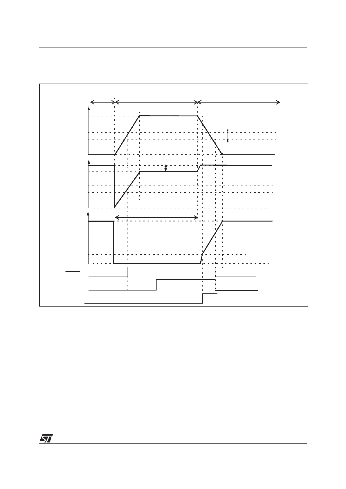
5.3.4.2 Gated mode
(TOUT = “0”, DOUT = “1”)
Figure 25. f
TIMER
Clock in Gated Mode
In this mode, the prescaler is decremented by the
Timer clock input, but only when the signal on the
TIMIO pin is held high (f
CPU
/16 gated by TIMIO).
See Figure 39 and Figure 40.
This mode is selected by clearing the TOUT bit in
the TSCR register (i.e. as input) and setting the
DOUT bit.
Figure 26. .Gated Mode Operation
f
TIMER
TIMIO
f
CPU
/16
f
EXT
xx1
1
Counter Value
TIMIO Pin
Timer Clock
Value 1
Value 2
Pulse Length
xx2
Page 37

ST72411R
37/71
8-BIT TIMER (Cont’d)
5.3.4.3 Event counter mode
(TOUT = “0”, DOUT = “0”)
Figure 27. f
TIMER
Clock in Event Counter Mode
In this mode, theTIMIO pin is the input clockof the
Timer prescaler which is decremented on every
rising edge of the input clock (allowing event
count). See Figure 41 and Figure 42.
This mode is selected by clearing the TOUT bit in
the TSCR register (i.e. as input) and clearing the
DOUT bit.
Figure 28. Event Counter Mode Operation
5.3.4.4 Output mode
(TOUT = “1”, DOUT = “data out”)
Figure 29. Output Mode Control
In Output mode, theTIMIO pin is connected to the
DOUT latch, hence the Timer prescaler isclocked
by the prescaler clock input (f
CPU
/16). See Figure
43.
The user can select the desired prescaler division
ratio through the PS1 and PS0 bits of the TSCR
register. When the TCR count underflows, it sets
the UDF bit in the TSCR. TheUDF bit can be tested under program control to perform a timer function whenever it goes high and has to be cleared
by the user. The low-to-high UDF bit transition is
used to latch the DOUT bit ofthe TSCR and, if the
OEN bit is set, DOUT is transferred to the TIMIO
pin. This operating mode allows external signal
generation on the TIMIO pin. See Figure 44.
This mode is selected by setting the TOUT bit in
the TSCR register (i.e. as output) and setting the
DOUT bit to output a high level or clearing the
DOUT bit to output a low level
Figure 30. Output Mode Operation
f
TIMER
TIMIO
xx1
Counter Value
TIMIO Pin
Value 1
Value 2
xx2
TIMIO
OEN DOUT UDF
LATCH
ALTERNATE
FUNCTION
TOUT DOUT
Timer
Function
Application
00
Event Counter
(input)
External counter clock
source
01
Gated input
(input)
External Pulse length
measurement
10
Output “0”
(output) Output signal
11
Output “1”
(output)
generation
FFh
1
Counter
TIMIO Pin
1
st
downcount :
Default output value is 0
At each underflow
DOUT has to be
copied to the TIMIO
pin
Page 38

ST72411R
38/71
8-BIT TIMER (Cont’d)
5.3.5 Register Description
PRESCALER COUNTER REGISTER (PSCR)
Read only
Reset Value: 1111 1111 (FFh)
Bit 7:0 = PSCR[8:1]
Prescaler MSB.
TIMER COUNTER REGISTER (TCR)
Read / Write
Reset Value: 1111 1111 (FFh)
Bit 7:0 = TCR[7:0]
Timer counter bits.
TIMER STATUS CONTROL REGISTER (TSCR)
Read/Write
Reset Value: 0101 0000 (50h)
Bit 7 = OEN
Output Enable.
In output mode, this bit allows DOUT to be send to
the timer output. It has no effects in INPUT mode.
0: Output disabled (reset state)
1: Output enabled
Bit 6 = TOUT
Timer Output Control.
When low, this bit selects the input mode for the
TIMER pin. When high the output mode is selected.
0: Input mode
1: Output mode (reset state)
Bit 5 = DOUT
Data Output.
Data sent to the timer output when UDF is set high
(output mode only). Input mode selection (input
mode only).
Bit 4 = UDF:
Timer Underflow.
A low-to-high transition indicates that the timer
count register has underflowed. It means that the
TCR value has changed from 00h to FFh.
This bit must be cleared by user software.
0: Counter has not underflowed
1: Counter underflow occurred (reset state)
Bit 3 = ETI:
Enable Timer Interrupt.
When set, enables the timer interrupt request. If
ETI=0 the timer interrupt is disabled. If ETI=1 and
UDF=1 an interrupt request is generated.
0: Interrupt disabled (reset state)
1: Interrupt enabled
Bit 2 = PSE:
Prescaler Enable.
Used to initialize the prescalerand inhibit itscounting. When PSE=“0” the prescaler is set to 1FFh
and the counter is inhibited. When PSE=“1” the
prescaler is enabled to count downwards. As long
as PSE=“0” both counter and prescaler are not
running
0: Counting disabled (reset state)
1: Counting enabled
Bit 1:0 = PS1:0
Prescaler Mux. Select.
These bits select the division ratio of the prescaler
register.
70
PSCR8 PSCR7 PSCR6 PSCR5 PSCR4 PSCR3 PSCR2 PSCR1
70
TCR7 TCR6 TCR5 TCR4 TCR3 TCR2 TCR1 TCR0
70
OEN TOUT DOUT UDF ETI PSE PS1 PS0
f
TIMER
divided by PS1 PS0
100
801
64 1 0
512 1 1
Page 39

ST72411R
39/71
8-BIT TIMER (Cont’d)
Table 10. 8-Bit Timer Register Map and Reset Values
Address
(Hex.)
Register Label 76543210
0031h
PSCR
Reset Value
PSCR81PSCR71PSCR61PSCR51PSCR41PSCR31PSCR21PSCR1
1
0032h
TCR
Reset Value
TCR71TCR61TCR51TCR41TCR31TCR21TCR11TCR0
1
0033h
TSCR
Reset Value
OEN
0
TOUT1DOUT0UDF
1
ETI
0
PSE
0
PS1
0
PS0
0
Page 40

ST72411R
40/71
5.4 32 x 4 LCD DRIVER
5.4.1 Introduction
The LCD driver controls up to 32 segments and 4
backplanes for driving up to 32x4 (128) LCD segments.
The LCD input clock can be divided by a selected
ratio depending on the required frame frequency.
The parameters todisplay arestored in a 16-bytes
LCD dual port RAM.
The peripheral can be switched off by software to
reduce power consumption when not in use.
No external capacitor/resistor network is required
as it is integrated on the chip.
Figure 31. LCD Driver Block Diagram
f
osc
/2
f
LCD
COM2
LCD RAM
32x4 bits
COM
MUX 128 to 32
f
LCD
COM[3:0]
DRIVERS
COM3
COM1
COM0
...
SEG
DRIVERS
SEG31
SEG0
f
LCD
COM[3:0]
Address Bus
Data Bus
V
DD
V
SS
SEG[31:0]
FREQUENCY
SELECTION
RING
COUNTER
REFERENCE VOLTAGE
GENERATOR
To COM and SEG Drivers
4
V
ss
2VDD/3V
DD
VDD/3
32
Page 41

ST72411R
41/71
LCD DRIVER (Cont’d)
5.4.2 Segment and Common signals
Each picture element of the LCD panel is turned
on when the differential voltage between the segment signal and the common signal rises above a
certain threshold voltage. It is turned off when the
voltage is below the threshold voltage.
Common signals determine the select timing within a frame cycle. The common signals have identical waveforms, but different phases. Each common signal has the highest amplitude only in the
corresponding phase ofa frame cycle. Atthe other
phases, the signal amplitude is lower (2/3 - 1/3). A
picture element can only be turned on with high
signal amplitude.
The LCD driver has 32x4 bits of display memory.
The corresponding address locations are read out
automatically in synchronisation with the select
timing of COM0, COM1, COM2and COM3.
Figure 32. Waveforms of LCD Outputs
5.4.3 Reference Voltages
The display voltage levels are supplied by aninternal resistor divider network as shown in Figure 47
This LCD driver generates 4 reference voltages
from VSSand VDDthrough an internal RC divider
network.
In order to increase current during transitions and
to reduce consumption in static state, tworesistive
networks are used. The high resistive divider is
permanently switched on during the LCD operation. The low resistive divider is only switched on
for a short period of time when the levels of common and segmentlines change. This method combines low source impedance for fast switching of
the LCD with high source impedance for low power consumption. When the LCD is disabled (bit
LCDEN=0), the internal resitive network is also
switched off for minimum power consumption.
Figure 33. LCD Reference Voltage generation
5.4.4 Display Example
The example in Figure 48 shows a sequence of
two identical frames containing the waveforms displaying a “4” in a seven-segment display.
In each T
FRAME
period, the LCD driver automatically switches on each of the fourCOM signalsfor
one T
LCD
period. COM0 is on in the first period,
COM1 in the second period and so on. To switch
them on,the waveform goes above and below the
threshold voltages. When the waveform is within
the thresholds, the COM is off.
The SEG signals are controlled by software by
programming the display memory.
– SEG 0 is off during the firstperiod and on for the
remaining three periods.
– SEG 1 is off duringT
LCD
periods 1, 2, and 4 and
on forT
LCD
period 3.
To program the display memory for this example,
software must write 00h in locations 0140h-0143h
and 01h in locations 144h through 0147h (refer to
Section 5.4.7)
V
DD
2/3
1/3
GND
COM ON
LCD clock
COM
i
COM OFF
V
DD
2/3
1/3
GND
SEG ON
SEG
i
SEG OFF
R
L
C
C
R
L
R
L
2VDD/3
V
DD
V
SS
R
H
R
H
R
H
RLON
LC DE
V
DD
V
SS
VDD/3
C
Page 42

ST72411R
42/71
LCD DRIVER (Cont’d)
Figure 34. Mux Waveforms Example
f
LCD
COM
0
V
DD
2/3
1/3
GND
COM
2
COM
3
SEG
1
T
FRAME
=4T
LCD
2/3
1/3
GND
COM0-SEG
0
V
DD
-2/3
-1/3
-V
DD
COM
1
2/3
1/3
GND
V
DD
-2/3
-1/3
-V
DD
COM1-SEG
0
COM ON
SEG OFF
COM OFF
SEG ON
COM OFF
SEG ON
COM OFF
SEGON
COM ON
SEG OFF
COM OFF
SEGON
COM OFF
SEG ON
COM OFF
SEG ON
COM OFF
SEG OFF
COMON
SEGON
COM OFF
SEG ON
COM OFF
SEGON
COM OFF
SEG OFF
COM ON
SEGON
COM OFF
SEG ON
COM OFF
SEGON
COM3
COM3
COM2
COM2
COM0
COM1
COM1
SEG0
SEG0
SEG0
SEG0
SEG1
SEG1
SEG1
Frame 1
Frame 2
SEG
0
V
DD
2/3
1/3
GND
V
DD
2/3
1/3
GND
V
DD
2/3
1/3
GND
V
DD
2/3
1/3
GND
V
DD
2/3
1/3
GND
Page 43

ST72411R
43/71
LCD DRIVER (Cont’d)
5.4.5 Clock generation
Figure 35. LCD Clock Generation Diagram
The frequency divider (FS[2:0]) should be chosen
according to the input frequency and the required
frame frequency,
A compromise should be found between a sufficient frame frequency display on the LCD for correct visualisation and a low frame frequency for
low consumption.
Below are the approximate LCD and frame frequencies resulting from the input frequencies selected using the FS[2:0] bits.
Note: The LCD frequency (f
LCD
) must not exceed
2kHz.
f
OSC
/2
3.58MHz
FS2 FS1 FS0 Ratio f
LCD
f
frame
1 1 1 16384 213.5Hz 53Hz
1 1 0 8192 427Hz 109Hz
1 0 1 4096 874Hz 218.5Hz
1 0 0 2048 1.748kHz 437Hz
f
OSC
/2
4MHz
FS2 FS1 FS0 Ratio f
LCD
f
frame
1 1 1 16384 244Hz 61Hz
1 1 0 8192 488Hz 122Hz
1 0 1 4096 977Hz 244Hz
1 0 0 2048 1.953kHz 488Hz
f
OSC
/2
----FS2FS1FS0LCDE
LCDCR
RATIO
DIVIDER
FS2 FS1 FS0
f
LCD
f
OSC
/2
2MHz
FS2 FS1 FS0 Ratio f
LCD
f
frame
1 1 0 8192 244Hz 61Hz
1 0 1 4096 488Hz 122Hz
1 0 0 2048 977Hz 244Hz
0 1 1 1024 1.953kHz 488Hz
f
OSC
/2
1MHz
FS2 FS1 FS0 Ratio f
LCD
f
frame
1 0 1 4096 244Hz 61Hz
1 0 0 2048 488Hz 122Hz
0 1 1 1024 977Hz 244Hz
0 1 0 512 1.953kHz 488Hz
f
OSC
/2
500kHz
FS2 FS1 FS0 Ratio f
LCD
f
frame
1 0 0 2048 244Hz 61Hz
0 1 1 1024 488Hz 122Hz
0 1 0 512 977Hz 244Hz
0 0 1 256 1.953kHz 488Hz
f
OSC
/2
225kHz
FS2 FS1 FS0 Ratio f
LCD
f
frame
0 1 1 1024 244Hz 61Hz
0 1 0 512 488Hz 122Hz
0 0 1 256 977Hz 244Hz
0 0 0 128 1.953kHz 488Hz
Page 44

ST72411R
44/71
LCD DRIVER (Cont’d)
5.4.6 Register Description
CONTROL REGISTER (CR)
Read/Write
Reset Value: 0000 0000 (00h)
Bit 7:4 = Reserved,
Must always be cleared
Bit 3:1 = FS2:0
Frame Frequency selection
These bits allow to select the LCD frame frequency. It controls the ratio between the input clock
(f
OSC
/2) and the LCD output clock (f
LCD
). These
bits are set and cleared by software.
Bit 0 = LCDE
LCD enable
This bit is set and cleared by software.
0: LCD disabled
1: LCD enabled
While the LCD is disabled (LCDE bit cleared), all
Segment and Common pins are high impedance.
5.4.7 LCD RAM Description
The 16-byte LCD RAM is located in memory from
address 0140h to address 014Fh. Each bit of the
LCD RAM is mapped to one picture element of the
LCD panel. If a bit is set, the corresponding picture
element is switched on, otherwise it is switched
off.
After reset, the LCD RAM is not initialized and its
content is indeterminate.
76543210
- - - - FS2 FS1 FS0 LCDE
Ration Divider FS2 FS1 FS0
1/16384 1 1 1
1/8192 1 1 0
1/4096 1 0 1
1/2048 1 0 0
1/1024 0 1 1
1/512 0 1 0
1/256 0 0 1
1/128 0 0 0
Addr. 76543210
COM0
0140h S7 S6 S5 S4 S3 S2 S1 S0
0141h S15 S14 S13 S12 S11 S10 S9 S8
0142h S23 S22 S21 S20 S19 S18 S17 S16
0143h S31 S30 S29 S28 S27 S26 S25 S24
COM1
0144h S7 S6 S5 S4 S3 S2 S1 S0
0145h S15 S14 S13 S12 S11 S10 S9 S8
0146h S23 S22 S21 S20 S19 S18 S17 S16
0147h S31 S30 S29 S28 S27 S26 S25 S24
COM2
0148h S7 S6 S5 S4 S3 S2 S1 S0
0149h S15 S14 S13 S12 S11 S10 S9 S8
014Ah S23 S22 S21 S20 S19 S18 S17 S16
014Bh S31 S30 S29 S28 S27 S26 S25 S24
COM3
014Ch S7 S6 S5 S4 S3 S2 S1 S0
014Dh S15 S14 S13 S12 S11 S10 S9 S8
014Eh S23 S22 S21 S20 S19 S18 S17 S16
014Fh S31 S30 S29 S28 S27 S26 S25 S24
Page 45

ST72411R
45/71
LCD DRIVER (Cont’d)
Table 11. LCD Driver Register Map and Reset Values
Address
(Hex.)
Register Label 76543210
0024h
LCDCR
Reset Value 0000
FS2
0
FS1
0
FS0
0
LCDE
0
0140h
to
014Fh
LCDRAM
Reset Value
Seg X
COMi
X
Seg X
COMi
X
Seg X
COMi
X
Seg X
COMi
X
Seg X
COMi
X
Seg X
COMi
X
SegX
COMi
X
Seg X
COMi
X
Page 46

ST72411R
46/71
5.5 SMARTCARD SUPPLY SUPERVISOR (SSS)
5.5.1 Introduction
The Smartcard Supply Supervisor (SSS) allows
the V
SC_PWR
Smartcard supply to be switched on
and off by software and protects the smartcard
from overload.
In addition, the SSS suppliespower to the I/O lines
used to interface the smartcard. This means that
no external components are needed for adapting
the interface to the levels required for interfacing
the smartcard,except a capacitor on the SC_PWR
output.
5.5.2 Main Features
■ Software power-on/off control
■ Hardware cut-off in case of output current
overload
■ Grounded output level when turned-off
■ Low consumption mode
5.5.3 General description
The SSS generates the Smartcard SC_PWR supply from the MCU VDDsupply. When disabled, the
regulator ties the output SC_PWR line to ground,
and is placed in low power mode. At the same
time, the interface I/O lines are also tied to ground.
In case of current overload on the output
SC_PWR, the output level drops due to internal
impedance of the regulator. The associated Current Overload detector switches-off the SC_PWR
supply and setsa flag into the Status/ControlRegister.
Figure 50 shows theSmartcard Supply Supervisor
(SSS) block diagram.
Figure 36. Smartcard Supply Supervisor (SSS) Block Diagram
Reference voltage
MCU V
DD
SC_PWR
+
-
SC I/Os
I/O
V
DD
SSSCR
+
-
V
DD
Reference Voltage
CURRENT OVERLOAD
VOLTAGE REGULATOR
OVLD
SSSR
OVLD
0 CKO D
CK_AF SSSOVLD
FOEN IE EN EN
3V
5V
1
0
f
OSC
/2
f
OSC
/4
0
1
SC_CK
OVLD INTERRUPT
Logic
Control
Logic
Control
DETECTOR
Page 47

ST72411R
47/71
SMARTCARD SUPPLY SUPERVISOR (Cont’d)
5.5.4 Functional Description
The core of the SSS is the internal reference voltage generator that is used for the output voltage
level regulation and for the Current Overload detection.
Output regulation is achieved from the MCU VDD
with a follower transistor used as output stage,associated to a feedback regulation.
Software control through the Status/Control register allows software to:
■ Turn-on / turn-off the SSS
■ Enable the overload detector
■ Enable interrupt in case of overload
Smartcard Power Supply
When disabled, the whole SSS is stopped in order
to achieve minimum consumption. The SC_PWR
line is tied to ground, and the I/O lines supplied by
SC_PWR, are also tied to ground.
When the SSS module is enabled, the SC_PWR
line provides a regulated voltage to the smartcard,
and the I/O lines have a logic “1” level identical to
the smartcard supply ensuring a safe interface.
Current Overload protection
When a current overload occurs on the SC_PWR
supply output, SC_PWR level drop is detected by
the Current Overload detector when enabled. As a
consequence, the SSS is turned-off with the
SC_PWR line tied to ground and the SSSEN bit is
cleared. On top of that, the OVLD flag is set into
the Status/Control Register and an interrupt request can be initiated.
Note: The Current Overload detector must be enabled by setting OVLDEN bit only after setting the
SSSEN bit.
Figure 37. Current Overload Detection
Switching SC_PWR from 3V to 5V output and
vice versa
The usual (and safe) procedure is to test the card
at 3V before selecting 5V output.
The applicationshould avoid making a direct transition from 5V to 3V as a delay is required before
the 3V level is reached (the delay depends onthe
external capacitor and card type).
For a controlled transition from 5V to 3V it is recommended to clear the SSSEN bit to tie the
SC_PWR to ground before enabling 3V output.
See Figure 52.
Figure 38. Recommended transitions when switching the voltage regulator (SSSR bit).
I
SC_PWR
0mA
0V
SHORT CIRCUIT
V
OVLD
OVLDF FLAG
V
SC_PWR
0V
V
SC_PWR
3V
5V
SSSR =0
SSSEN=1
SSSR=1
SSSEN=1
SSSR=1
SSSEN=0
SSSR=0
SSSEN=1
t
Page 48

ST72411R
48/71
SMARTCARD SUPPLY SUPERVISOR (Cont’d)
5.5.5 Register Description
CONTROL/STATUS REGISTER (SSSCR)
Read/Write
Reset Value: 0000 0000 (00h)
Bit 7 = Reserved, forced by hardware to 0.
Bit 6 = CKOD
Clock output division
This bit is set and cleared by software. It selects
the frequency division factor of the SC_CK output
clock.
0: SC_CK clock output frequency = f
osc
/2.
1: SC_CK clock output frequency = f
osc
/4.
Bit 5 = CK_AFOEN
Clock AF output enable
This bit is set and cleared by software.
0: The SC_CK alternate function is disabled. The
I/O port is free for general purpose I/O.
1: The SC_CK alternate function is enabled. The
clock is output on the I/O port.
Bit 4 = OVLDF
Overload flag
This bit is set byhardware when theSC_PWR output voltage drops due to current overload. It is set
when a falling edge is detected on SC_PWR and
when SC_PWR is under the Overload Voltage
Level. This bit can only be cleared by software.
0: No Current Overload
1: Current Overload
Bit 3 = OVLDIE
Overload interrupt enable
This bit is set andcleared by software.
0: OVLD interrupt disabled.
1: OVLD interrupt enabled.
Bit 2= OVLDEN
Current overload detector enable
This bit is set and cleared by software. This bit
must be set only when SSSEN =1.
0: Current Overload Detection disabled.
1: Current Overload Detection enabled.
Bit 1 = SSSR
Smartcard supply regulation
This bit is set and cleared by software. Refer to
Figure 52 for recommended transitions.
0: The regulation voltage output is 3V.
1: The regulation voltage output is 5V.
Bit 0 = SSSEN
SSS module enable
This bit can only be set by software. It can be
cleared by software. It is cleared by hardware
when OVLDF=1 (current overload condition).
0: SSS is disabled.
1: SSS is enabled.
76543210
0 CKOD
CK_A
FOEN
OVLDF
OV-
LDIE
OV-
LDEN
SSSR
SS-
SEN
Page 49

ST72411R
49/71
SMARTCARD SUPPLY SUPERVISOR (Cont’d)
Table 12. SSSCR Register Map and Reset Values
Address
(Hex.)
Register
Name
76543210
0025h
SSSCR
Reset Value
0
CKD0CK_AFOEN0OVLDF0OVLDIE0OVLDEN0SSSR
0
SSSEN
0
Page 50

ST72411R
50/71
6 INSTRUCTION SET
6.1 ST7 ADDRESSING MODES
The ST7 Core features 17 different addressing
modes which can be classified in 7 main groups:
The ST7 Instruction set is designed to minimize
the numberof bytes required per instruction: To do
so, most of the addressing modes may be subdivided in two sub-modes called long and short:
– Long addressing mode is more powerful be-
cause itcan usethe full 64 Kbyte address space,
however it uses more bytes and moreCPU cycles.
– Short addressing modeis less powerfulbecause
it can generally only access page zero (0000h 00FFh range), but the instruction size ismore
compact, and faster. All memory to memory instructions use short addressing modes only
(CLR, CPL, NEG, BSET, BRES, BTJT, BTJF,
INC, DEC, RLC, RRC, SLL, SRL, SRA, SWAP)
The ST7Assembler optimizes the use of long and
short addressing modes.
Table 13. ST7 Addressing Mode Overview
Note 1. At the time the instruction is executed, the Program Counter (PC) points to the instruction following JRxx.
Addressing Mode Example
Inherent nop
Immediate ld A,#$55
Direct ld A,$55
Indexed ld A,($55,X)
Indirect ld A,([$55],X)
Relative jrne loop
Bit operation bset byte,#5
Mode Syntax
Destination/
Source
Pointer
Address
(Hex.)
Pointer
Size
(Hex.)
Length
(Bytes)
Inherent nop + 0
Immediate ld A,#$55 + 1
Short Direct ld A,$10 00..FF + 1
Long Direct ld A,$1000 0000..FFFF + 2
No Offset Direct Indexed ld A,(X) 00..FF
+ 0 (with X register)
+ 1 (with Y register)
Short Direct Indexed ld A,($10,X) 00..1FE + 1
Long Direct Indexed ld A,($1000,X) 0000..FFFF + 2
Short Indirect ld A,[$10] 00..FF 00..FF byte + 2
Long Indirect ld A,[$10.w] 0000..FFFF 00..FF word + 2
Short Indirect Indexed ld A,([$10],X) 00..1FE 00..FF byte + 2
Long Indirect Indexed ld A,([$10.w],X) 0000..FFFF 00..FF word + 2
Relative Direct jrne loop PC-128/PC+127
1)
+1
Relative Indirect jrne [$10] PC-128/PC+127
1)
00..FF byte + 2
Bit Direct bset $10,#7 00..FF + 1
Bit Indirect bset [$10],#7 00..FF 00..FF byte + 2
Bit Direct Relative btjt $10,#7,skip 00..FF + 2
Bit Indirect Relative btjt [$10],#7,skip 00..FF 00..FF byte + 3
Page 51

ST72411R
51/71
ST7 ADDRESSING MODES (Cont’d)
6.1.1 Inherent
All Inherent instructions consist of a single byte.
The opcode fullyspecifies all the required information for the CPU to process the operation.
6.1.2 Immediate
Immediate instructions have two bytes, the first
byte contains the opcode, the second byte contains the operand value.
6.1.3 Direct
In Direct instructions, the operands are referenced
by their memory address.
The direct addressing mode consists of two submodes:
Direct (short)
The addressis a byte, thusrequires only one byte
after the opcode, but only allows 00 - FF addressing space.
Direct (long)
The addressis a word, thus allowing 64 Kbyte addressing space, but requires 2 bytes after the opcode.
6.1.4 Indexed (No Offset, Short, Long)
In this mode, the operand is referenced by its
memory address, which is defined by the unsigned
addition of an index register (X or Y) with an offset.
The indirect addressing mode consists of three
sub-modes:
Indexed (No Offset)
There is no offset, (no extra byteafter theopcode),
and allows 00 - FF addressing space.
Indexed (Short)
The offset isa byte, thus requires only one byte after the opcode and allows 00 - 1FE addressing
space.
Indexed (long)
The offset is a word, thus allowing 64 Kbyte addressing space and requires 2 bytes after the opcode.
6.1.5 Indirect (Short, Long)
The required data byte to do the operation is found
by its memory address, located in memory (pointer).
The pointer address follows the opcode. The indirect addressing mode consists of two sub-modes:
Indirect (short)
The pointer address is a byte, the pointer size is a
byte, thus allowing 00 - FF addressing space, and
requires 1 byte after the opcode.
Indirect (long)
The pointer address is a byte, the pointer size is a
word, thus allowing 64 Kbyte addressing space,
and requires 1 byte after the opcode.
Inherent Instruction Function
NOP No operation
TRAP S/W Interrupt
WFI
Wait For Interrupt (Low Power
Mode)
HALT
Halt Oscillator (Lowest Power
Mode)
RET Sub-routine Return
IRET Interrupt Sub-routine Return
SIM Set Interrupt Mask
RIM Reset Interrupt Mask
SCF Set Carry Flag
RCF Reset Carry Flag
RSP Reset Stack Pointer
LD Load
CLR Clear
PUSH/POP Push/Pop to/from the stack
INC/DEC Increment/Decrement
TNZ Test Negative or Zero
CPL, NEG 1 or 2 Complement
MUL Byte Multiplication
SLL, SRL, SRA, RLC,
RRC
Shift and Rotate Operations
SWAP Swap Nibbles
Immediate Instruction Function
LD Load
CP Compare
BCP Bit Compare
AND, OR, XOR Logical Operations
ADC, ADD, SUB, SBC Arithmetic Operations
Page 52

ST72411R
52/71
ST7 ADDRESSING MODES (Cont’d)
6.1.6 Indirect Indexed (Short, Long)
This is a combination of indirect and short indexed
addressing modes. The operand is referenced by
its memory address, which is defined by the unsigned addition of an index register value (X or Y)
with a pointer value located in memory. The pointer address follows the opcode.
The indirect indexed addressing mode consists of
two sub-modes:
Indirect Indexed (Short)
The pointer address is a byte, the pointer size is a
byte, thus allowing 00 - 1FE addressing space,
and requires 1 byte after the opcode.
Indirect Indexed (Long)
The pointer address is a byte, the pointer size is a
word, thus allowing 64 Kbyte addressing space,
and requires 1 byte after the opcode.
Table 14. Instructions Supporting Direct,
Indexed, Indirect and Indirect Indexed
Addressing Modes
6.1.7 Relative mode (Direct, Indirect)
This addressing mode is used to modify the PC
register value, by adding an 8-bit signed offset to
it.
The relative addressing mode consists oftwo submodes:
Relative (Direct)
The offset follows the opcode.
Relative (Indirect)
The offset is defined in memory, of which the address follows the opcode.
Long and Short
Instructions
Function
LD Load
CP Compare
AND, OR, XOR Logical Operations
ADC, ADD, SUB, SBC
Arithmetic Addition/subtraction operations
BCP Bit Compare
Short Instructions Only Function
CLR Clear
INC, DEC Increment/Decrement
TNZ Test Negative orZero
CPL, NEG 1 or 2 Complement
BSET, BRES Bit Operations
BTJT, BTJF
Bit Test and Jump Operations
SLL, SRL, SRA, RLC,
RRC
Shift and Rotate Operations
SWAP Swap Nibbles
CALL, JP Call or Jump subroutine
Available Relative Direct/
Indirect Instructions
Function
JRxx Conditional Jump
CALLR Call Relative
Page 53

ST72411R
53/71
6.2 INSTRUCTION GROUPS
The ST7 family devices use an Instruction Set
consisting of 63 instructions. The instructions may
be subdivided into 13 main groups as illustrated in
the following table:
Using a pre-byte
The instructions are described with one to four
bytes.
In order to extend the number of available opcodes for an 8-bit CPU (256opcodes), three different prebyte opcodes are defined. These prebytes
modify the meaning of the instruction they precede.
The whole instruction becomes:
PC-2 End of previous instruction
PC-1 Prebyte
PC opcode
PC+1 Additional word (0 to 2) according
to the number of bytesrequired to compute the effective address
These prebytes enable instruction in Y as well as
indirect addressing modes to be implemented.
They precedethe opcode of the instruction in X or
the instruction using direct addressing mode. The
prebytes are:
PDY 90 Replace an X based instruction
using immediate, direct, indexed, or inherent addressing mode by a Y one.
PIX 92 Replace an instruction using direct, direct bit, or direct relative addressing mode
to an instruction using the corresponding indirect
addressing mode.
It also changes an instruction using X indexed addressing mode to aninstruction usingindirect Xindexed addressing mode.
PIY 91 Replace an instruction using X indirect indexed addressing mode by a Y one.
Load and Transfer LD CLR
Stack operation PUSH POP RSP
Increment/Decrement INC DEC
Compare and Tests CP TNZ BCP
Logical operations AND OR XOR CPL NEG
Bit Operation BSET BRES
Conditional Bit Test and Branch BTJT BTJF
Arithmetic operations ADC ADD SUB SBC MUL
Shift and Rotates SLL SRL SRA RLC RRC SWAP SLA
Unconditional Jump or Call JRA JRT JRF JP CALL CALLR NOP RET
Conditional Branch JRxx
Interruption management TRAP WFI HALT IRET
Code Condition Flag modification SIM RIM SCF RCF
Page 54

ST72411R
54/71
INSTRUCTION GROUPS (Cont’d)
Mnemo Description Function/Example Dst Src H I N Z C
ADC Add with Carry A = A + M + C A M H N Z C
ADD Addition A = A + M A M H N Z C
AND Logical And A = A . M A M N Z
BCP Bit compare A, Memory tst (A . M) A M N Z
BRES Bit Reset bres Byte, #3 M
BSET Bit Set bset Byte, #3 M
BTJF Jump if bit is false (0) btjf Byte, #3, Jmp1 M C
BTJT Jump if bit is true (1) btjt Byte, #3, Jmp1 M C
CALL Call subroutine
CALLR Call subroutine relative
CLR Clear reg, M 0 1
CP Arithmetic Compare tst(Reg - M) reg M N Z C
CPL One Complement A = FFH-A reg, M N Z 1
DEC Decrement dec Y reg, M N Z
HALT Halt 0
IRET Interrupt routine return Pop CC, A, X, PC H I N Z C
INC Increment inc X reg, M N Z
JP Absolute Jump jp [TBL.w]
JRA Jump relative always
JRT Jump relative
JRF Never jump jrf *
JRIH Jump if ext. interrupt = 1
JRIL Jump if ext. interrupt = 0
JRH Jump if H = 1 H = 1 ?
JRNH Jump if H = 0 H = 0?
JRM Jump if I = 1 I = 1 ?
JRNM Jump if I = 0 I = 0 ?
JRMI Jump if N = 1 (minus) N = 1 ?
JRPL Jump if N = 0 (plus) N = 0 ?
JREQ Jump if Z = 1 (equal) Z = 1 ?
JRNE Jump if Z = 0 (not equal) Z = 0 ?
JRC Jump if C = 1 C = 1 ?
JRNC Jump if C = 0 C = 0?
JRULT Jump if C = 1 Unsigned <
JRUGE Jump if C = 0 Jmp if unsigned >=
JRUGT Jump if (C + Z = 0) Unsigned >
Page 55

ST72411R
55/71
INSTRUCTION GROUPS (Cont’d)
Mnemo Description Function/Example Dst Src H I N Z C
JRULE Jump if (C + Z = 1) Unsigned <=
LD Load dst <= src reg, M M, reg N Z
MUL Multiply X,A = X * A A, X, Y X, Y, A 0 0
NEG Negate (2’s compl) neg $10 reg, M N Z C
NOP No Operation
OR OR operation A = A + M A M N Z
POP Pop from the Stack pop reg reg M
pop CC CC M H I N Z C
PUSH Push onto the Stack push Y M reg, CC
RCF Reset carry flag C = 0 0
RET Subroutine Return
RIM Enable Interrupts I = 0 0
RLC Rotate left true C C <= Dst <= C reg, M N Z C
RRC Rotate right true C C => Dst => C reg, M N Z C
RSP Reset Stack Pointer S = Max allowed
SBC Subtract with Carry A = A - M - C A M N Z C
SCF Set carry flag C = 1 1
SIM Disable Interrupts I = 1 1
SLA Shift left Arithmetic C <= Dst <= 0 reg, M N Z C
SLL Shift left Logic C <= Dst <= 0 reg, M N Z C
SRL Shift right Logic 0 => Dst => C reg, M 0 Z C
SRA Shift right Arithmetic Dst7 => Dst => C reg, M N Z C
SUB Subtraction A = A - M A M N Z C
SWAP SWAP nibbles Dst[7..4] <=> Dst[3..0] reg, M N Z
TNZ Test for Neg & Zero tnz lbl1 N Z
TRAP S/W trap S/W interrupt 1
WFI Wait for Interrupt 0
XOR Exclusive OR A = A XOR M A M N Z
Page 56

ST72411R
56/71
7 ELECTRICAL CHARACTERISTICS
7.1 ABSOLUTE MAXIMUM RATINGS
This product contains devicesfor protecting the inputs against damage due to high static voltages,
however it is advisable to take normal precautions
to avoid appying any voltage higher than the specified maximum rated voltages.
For proper operation it is recommended that V
I
and VObe higher than VSSand lower than VDD.
Reliability is enhanced if unused inputs are connected to an appropriate logic voltage level (V
DD
or VSS).
Power Considerations. The average chip-junction temperature, TJ, in Celsius can be obtained
from:
TJ= TA + PD x RthJA
Where: TA= Ambient Temperature.
RthJA =Package thermal resistance
(junction-to ambient).
PD=P
INT+PPORT
.
P
INT
=IDDxVDD(chip internal power).
P
PORT
=Portpower dissipation
determined by the user)
Note: Stresses above those listed as “absolute maximum ratings” may cause permanent damage to the device. This is
a stress rating only and functional operation of thedevice at these conditions is not implied. Exposure tomaximum rating
conditions for extended periods may affect device reliability.
General Warning: Direct connection to V
DD
or VSSof the RESET and I/O pins could damage the device in case of program counter corruption (due to unwanted change of the I/O configuration). To guarantee safeconditions, this connection
has to be done through a typical 10KΩ pull-up or pull-down resistor.
Thermal Characteristics
Symbol Ratings Value Unit
V
DD-VSS
Supply voltage 7.0 V
V
IN
Input voltage VSS- 0.3 to VDD+ 0.3 V
V
OUT
Output voltage VSS- 0.3 to VDD+ 0.3 V
ESD ESD susceptibility 3500 V
I
VDD_i
Total current into V
DD_i
(source) 150
mA
I
VSS_i
Total current out of V
SS_i
(sink) 150
Symbol Ratings Value Unit
R
thJA
Package thermal resistance TQFP64
EQFP64
60
N/A
°C/W
T
Jmax
Max. junction temperature 150 °C
T
STG
Storage temperature range -65 to +150 °C
PD Power dissipation 500 mW
Page 57

ST72411R
57/71
7.2 RECOMMENDED OPERATING CONDITIONS
Figure 39. Maximum Operating Frequency (f
OSC
) Versus Supply Voltage (VDD)
(Operating conditions TA= 0 to +70°C unless otherwise specified)
GENERAL
Symbol Parameter Conditi ons Min Typ Max Unit
V
DD
Supply voltage see Figure 39 4.0 6.6 V
f
RCINT
Internal oscillator frequency 7.16 ±25%
MHz
f
OSC
External clock source >0 8
T
A
Ambient temperature range 0 70 °C
I
26&
>0+]@
Main Supply Voltage
[V
DD
]
FUNCTIONALITY NOT GUARANTEED INTHIS AREA
FUNCTIONALITY GUARANTE ED IN THIS AREA WITH FOR 3V CARDS ONLY (ISO/IEC7816-3 CLASS B)
FUNCTIONALITY GUARANTEEDIN THIS AREA
FOR 3V AND 5V CARDS
f
RCINT
Page 58

ST72411R
58/71
RECOMMENDED OPERATING CONDITIONS (Cont’d)
(Operating conditions TA= 0 to +70°C unless otherwise specified)
Note 1: Positive injection
The I
INJ+
is done through protection diodes insulated from the substrate of the die.
Note 2: For SC I/Os, VSC_PWR has to be considered.
Note 3: Negative injection
– The I
INJ-
is done through protection diodes NOT INSULATED from the substrate of the die. The drawback is asmall leakage (few µA) inducedinside the diewhen a negative injection isperformed. This leakage is tolerated by the digital structure, but it acts on theanalog line according to theimpedance versus
a leakage current of few µA (if the MCU has an AD converter). The effect depends on the pin which is
submitted to the injection. Of course, external digitalsignals appliedto the component must have a maximum impedance close to 50KΩ.
Location of the negative current injection:
– Puredigital pins cantolerate 1.6mA. In addition, the best choice is to inject the current as far as possible
from the analog input pins.
General Note: When several inputs are submitted to a current injection, the maximum I
INJ
is the sum of
the positive (resp. negative) currrents (instantaneous values).
CURRENT INJECTION ON I/O PORT AND CONTROL PINS
Symbol Parameter Conditi ons Min Typ Max Unit
I
INJ+
Total positive injected current
(1)
V
EXTERNAL>VDD
(Standard I/Os)
V
EXTERNAL>VSC_PWR
(Smart card I/Os)
5* mA
I
INJ-
Total negative injected current
(2)
V
EXTERNAL<VSS
Digital pins
Analog pins
1.6
0.8
mA
Page 59

ST72411R
59/71
RECOMMENDED OPERATING CONDITIONS (Cont’d)
(TA=0 to +70oC, VDD-VSS=6V unless otherwise specified)
Notes:
1. CPU running with memory access, all I/O pins in input mode with a static value at V
DD
or VSS; clock input (OSC1)
driven by external square wave, LVD enabled.
2. All I/O pins in input mode with a static value at V
DD
or VSS; clock input (OSC1) driven by external square wave, LVD
enabled.
3. WAIT Mode with SLOW Mode selected, LVD enabled. Based on characterisation results, not tested.
4. All I/O pins in input mode with a static value at V
DD
or VSS, I/O PORT CHARACTERISTICS
T = 0... +70oC, voltages are referred to VSSunless otherwise specified:
* Note: Hysteresis voltage between Schmitt trigger switching levels. Based on characterisation results, not tested.
Symbol Parameter Conditions Min Typ. Max Unit
I
DD
Supply current in RUN mode
1)
f
OSC
=8MHz
36mA
Supply current in SLOW mode
1)
0.4 mA
Supply current in WAIT mode
2)
0.6 mA
Supply current inSLOW WAIT mode
3)
0.3 mA
Supply current in HALT mode, LVD enabled.
4)
I
LOAD
= 0mA 300 µA
Supply current inHALT mode LVD disabled.
4)
0 µA
I/O PORT PINS
Symbol Parameter Conditions Min Typ Max Unit
V
IL
Input low level voltage 0.3xV
DD
V
V
IH
Input high level voltage 0.7xV
DD
V
HYS
Schmidt trigger voltage hysteresis * 400 mV
V
OL
Output low level voltage
for Standard I/O port pins
I=-5mA 1.3
V
I=-2mA 0.4
V
OH
Output high level voltage
I=5mA V
DD
-1.3
I=2mA V
DD
-0.4
I
L
Input leakage current VSS<V
PIN<VDD
1
µA
I
SV
Static current consumption Floating input mode 200
R
PU
Pull-up equivalent resistor
V
IN>VIH
VIN<V
IL
20
60
40
120
80
240
KΩ
R
PD
Pull-down equivalent resistor (PB6)
V
IN>VIH
VIN<V
IL
20
60
40
120
80
240
KΩ
t
OHL
Output high to low level fall time
for Standard I/O port pins
C
l
=50pF 14.8 25 45.6
nsOutput high to low level fall time
for high sink I/O port pins
TBD TBD TBD
t
OLH
Output L-H rise time Cl=50pF 14.4 25 45.9
t
ITEXT
External interrupt pulse time 1 t
CPU
Page 60

ST72411R
60/71
7.3 SUPPLY, RESET AND CLOCK CHARACTERISTICS
(T = 0 to +70oC, VDD-VSS= 6 V unless otherwise specified.
Note *: the V
hys
hysteresis is constant.
7.4 TIMING CHARACTERISTICS
(Operating conditions TA= 0 to +70°C unless otherwise specified)
* ∆t
INST
is the number of t
CPU
to finish the current instruction execution.
LOW VOLTAGE DETECTOR AND SUPERVISOR (LVDS)
Symbol Parameter Conditions Min Typ Max Unit
V
IT+
Reset release threshold
(V
DD
rising)
3.7 V
V
IT-
Reset generation threshold
(V
DD
falling)
3.2 V
V
hys
Hysteresis V
IT+-VIT-
500* mV
RESET SEQUENCE MANAGER (RSM)
Symbol Parameter Conditions Min Typ Max Unit
R
ON
Reset weak pull-up resistance
V
IN>VIH
VIN<V
IL
20
60
40
120
80
240
kΩ
t
PULSE
External RESET pin Pulse time 20 µs
Symbol Parameter Conditi ons Min Typ Max Unit
t
INST
Instruction time 2 12 t
CPU
t
IRT
Interrupt reaction time t
IRT
= ∆t
INST
+ 10* 10 22 t
CPU
Page 61

ST72411R
61/71
7.5 MEMORY CHARACTERISTICS
Subject to general operating conditions for VDD,f
OSC
, and TAunless otherwise specified.
7.5.1 RAM and Hardware Registers
7.5.2 FLASH Program Memory
Notes:
1. Minimum V
DD
supply voltage without losing data stored in RAM (in in HALT mode or under RESET) or in hardware
registers (only in HALT mode). Guaranteed by construction, not tested in production.
2. Up to 16 bytes can be programmed at a time for a 4kBytes FLASH block
3. The data retention time increases when the T
A
decreases.
4. Data based on reliability test results and monitored in production.
7.6 LCD ELECTRICAL CHARACTERISTICS
Absolute Maximum Ratings (Voltage Referenced to VSS)
Note: Electrical simulations on design database and product characterization will be done over [0 to
+70°C] temperature range.
(T = 0... +70oC, VDD-VSS= 6 V unless otherwise specified)
Notes:
1) The DC offset voltage refers to all segment and common outputs. It is the interface between the measured voltage
value and nominal value for every voltage level. Ri of voltage meter must be greater than or equal to 10MW.
2) Target value to be confirmed after product characterisation.
Symbol Parameter Conditi ons Min Typ Max Unit
V
RM
Data retention mode
1)
HALT mode (or RESET) 1.6 V
Symbol Parameter Conditions Min Typ Max Unit
t
prog
Programming time for 1~16 bytes2)TA=+25°C825ms
Programming time for 4 KBytes
T
A
=+25°C 2.1 6.4
sec
t
ret
Data retention
4)
TA=+55°C
3)
20 years
N
RW
Write erase cycles
4)
TA=+25°C 100 cycles
Symbol Ratings Value Unit
V
LCD
Max. Display Voltage
Note: V
LCD=VDD
6.6 V
I
VDDP_i-IVSSP_i
Total current into V
DDP_i/VSSP_i
80/80 mA
LCD DRIVER
Symbol Parameter Conditions Min
(2)
Typ
(2)
Max
(2)
Unit
f
FR
Frame frequency
f
RCINT
=7.16 MHz 53 437 Hz
f
OSC
=8 MHz 61 488 Hz
V
OS
DC Offset Voltage
(1)
V
LCD=VDD
no load 50 mV
V
COH
COM High Level, Output Voltage I=100µA, V
LCD
=5V 4.5 V
V
COL
COM Low Level, Output Voltage I=50µA, V
LCD
=5V 0.5 V
V
SOH
SEG High Level, Output Voltage I=50µA, V
LCD
=5V 4.5 V
V
SOL
SEG Low Level, Output Voltage I=100µA, V
LCD
=5V 0.5 V
V
LCD
Display Voltage V
LCD=VDD
4.5 6.6 V
C
LOAD
LCD dot Load 50 pF
Page 62

ST72411R
62/71
7.7 SMARTCARD SUPPLY SUPERVISOR ELECTRICAL CHARACTERISTICS
(TA= 0... +70oC, VDD-VSS= 6 V unless otherwise specified)
Figure 40. ISCLoad with 5V Regulator Output (for IEC7816-3 Class A Cards)
SMARTCARD SUPPLY SUPERVISOR
Symbol Parameter Conditions Min Typ Max Unit
SSS DRIVER bit SSR=1 : 5V regulator output (for IEC7816-3 Class A Cards)
V
SC_PWR
SmartCard Power Supply Voltage VDD-VSS>V
SC_PWR
+0.5V 4.5 5.00 5.5 V
I
SC
SmartCard Supply Current
V
DD-VSS
= 5.5V,
V
SC_PWR
=4.5V
30 mA
V
DD-VSS
=6V,
V
SC_PWR
=4.8V
60 mA
V
OVLD
Voltage Drop Threshold on Current
Overload
V
DD-VSS
= 6V, R
VDD
=0V 3.85 V
SSS DRIVER bit SSR=0 : 3V regulator output (for IEC7816-3 Class B Cards)
V
SC_PWR
SmartCard Power Supply Voltage 2.7 3.00 3.3 V
I
SC
SmartCard Supply Current
V
DD-VSS
= 3.5V TBD
V
DD-VSS
= 4.5V 30 mA
V
DD-VSS
=5V 50 mA
V
OVLD
Voltage Drop Threshold on Current
Overload
V
DD-VSS
= 6V, R
VDD
=0V 2.4 V
T
off
VSCTurn off Time C
LOADmax
=20uF 200 us
T
on
VSCTurn on Time C
LOADmax
=20uF 200 us
Smart Card I/O Pins
V
IL
Input Low Level Voltage - - 0.3V
SCPWR
V
V
IH
Input High Level Voltage 0.7V
SCPW R
--V
V
OL
Output Low Level Voltage I=-2.6mA - - TBD V
V
OH
Output High Level Voltage I=2.6mA TBD - - V
I
L
Input Leakage Current VSS<VIN<V
SC_PWR
-10 - 10 µA
I
RPU
Pull-up Equivalent Resistance VIN=V
SS
40 - 250 KΩ
T
OHL
Output H-L Fall Time Cl=50pF - 30 - ns
T
OLH
Output L-H Rise Time Cl=50pF - 30 - ns
V
SC_PWR
Load
[mA]
5.0
4.5
4.0
I
SC
5.5
3.5
10 20 30 40 50 60 70
VDD=6VVDD=5.5V
VDD=6.5V
IEC7816-3 Spec
Page 63

ST72411R
63/71
Figure 41. ISCLoad with 3V Regulator Output (for IEC7816-3 Class B Cards)
V
SC_PWR
Load
[mA]
3.0
2.5
2.0
I
SC
3.5
10 20 30 40 50 60 70
VDD=5V
VDD=4.5V
IEC7816-3 Spec
Page 64

ST72411R
64/71
8 DEVICE CONFIGURATION
Each deviceis availablefor production in user programmable versions (FLASH) as well as in factory
coded versions (ROM). FLASH devices are
shipped to customers with a default content (FFh),
while ROM factory coded parts contain the code
supplied by the customer. Thisimplies that FLASH
devices have tobe configuredby the customer using the Option Bytes while the ROM devices are
factory-configured.
8.1 OPTION BYTE
The option byte allows the hardware configuration
of the microcontroller to be selected.
The option bytes have no address in the memory
map and can be accessed only in programming
mode (for example using a standard ST7 programming tool). The default content of the FLASH is
fixed to FFh.
In masked ROM devices, the option bytes are
fixed in hardware by the ROM code (see option
list).
Bit 7:1 = Reserved, must always be 1.
Bit 0 = FMP
Full memory protection.
This option bit enablesor disablesexternal access
to the internal program memory (read-out protection). Clearing this bit causes the erasing (to 00h)
of the whole memory (including the option byte).
0: Program memory not read-out protected
1: Program memory read-out protected
OPTION BYTE
70
Reserved FMP
Default
Value
11111110
Page 65

ST72411R
65/71
9 GENERAL INFORMATION
9.1 PACKAGE MECHANICAL DATA
Figure 42. 64-Pin Thin Quad Flat Package
Figure 43. 64-Pin Epoxy Thin Quad Flat Package
Note: “ QUALIFICATION OR VOLUME PRODUCTION OF DEVICES USING EPOXYPACKAGES
(ESO/EDIL/EQFP) IS NOT AUTHORIZED It is expressly specified that qualification and/or volume production of devices
using the package E.... in any applications is not authorized. Usage in any application is strictly restricted to development
purpose. Similar devices are available inplastic package mechanically compatible to the epoxy package forqualification
and volume production.”
Dim
mm inches
Min Typ Max Min Typ Max
A 1.60 0.063
A1 0.05 0.15 0.002 0.006
A2 1.35 1.40 1.45 0.053 0.055 0.057
B 0.30 0.37 0.45 0.012 0.015 0.018
C 0.09 0.20 0.004 0.008
D 16.00 0.630
D1 14.00 0.551
D3 12.00 0.472
E 16.00 0.630
E1 14.00 0.551
E3 12.00 0.472
e 0.80 0.031
K 0° 3.5° 7°
L 0.45 0.60 0.75 0.018 0.024 0.030
L1 1.00 0.039
Number of Pins
N 64 ND 16 NE 16
L1
L
K
Dim
mm inches
Min Typ Max Min Typ Max
A 2.40 0.095
A1 0.60 0.024
B 0.25 0.38 0.50 0.010 0.015 0.020
E 15.80 16.00 16.20 0.622 0.630 0.638
E1 12.20 12.35 12.50 0.480 0.486 0.492
e 0.80 0.031
G 13.10 0.515
L 0.50 0.020
L1 1.10 0.043
∅n 0.35 0.013
∅P 1.10 0.043
Number of Pins
N 64 (4x16)
ETQFP64
L1 L
∅n
B
∅P
e
G
A1
A
Page 66

ST72411R
66/71
PACKAGE MECHANICAL DATA (Cont’d)
Figure 44. Recommended Reflow Oven Profile (MID JEDEC)
9.2 ADAPTOR / SOCKET PROPOSAL
To solder the (E)TQFP64 package or to plug the
emulator probe, the application board should provide thefootprint described in Figure 45. This footprint allows the following connexion configurations:
■ Direct (E)TQFP64 soldering
■ YAMAICHI IC149-064-008-S5* socket
soldering to plug either the emulatorprobe or an
adaptator board with an (E)TQFP64 clamshell
socket delivered with the emulator.
* Not compatible with (E)TQFP64 package.
Figure 45. (E)TQFP64 device and emulation probe compatible footprint
250
200
150
100
50
0
100 200 300 400
Time [sec]
Temp. [°C]
ramp up
2°C/sec for 50sec
90 sec at 125°C
150 sec above 183°C
ramp down natural
2°C/sec max
Tmax=220+/-5°C
for 25 sec
DETAIL
e
B
* SK: Plastic socket overall dimensions.
Dim
mm inches
Min Typ Max Min
Typ Max
B 0.35 0.45 0.50 0.014 0.018 0.020
E 20.80 0.819
E1 14.00 0.551
E3 11.90 12.00 12.10 0.468 0.472 0.476
e 0.75 0.80 0.85 0.029 0.031 0.033
SK* 26 1.023
Number of Pins
N 64 (4x16)
E
E1
E3
E
E1
E3
62 &. ( 7
SK
SK
Page 67

ST72411R
67/71
9.3 DEVELOPMENT TOOLS
STmicroelectronics offers a range of hardware
and software development tools for the ST7 microcontroller family. Full details of tools available for
the ST7 from third party manufacturers can be obtain from the STMicroelectronics Internet site:
➟ http//mcu.st.com.
Third Party Tools
■ ACTUM
■ BP
■ COSMIC
■ CMX
■ DATA I/O
■ HITEX
■ HIWARE
■ ISYSTEM
■ KANDA
■ LEAP
Tools from these manufacturers include C compliers, emulatorsand gang programmers.
STMicroelectronics Tools
Three types of development tool are offered by
ST, all of them connectto a PC via a parallel (LPT)
port: see Table 15 and Table 16 for more details.
Table 15. STMicroelectronic Tool Features
Table 16. Dedicated STMicroelectronics Development Tools
Note:
1. In-Situ Programming (ISP) interface for FLASH devices.
In-Circuit Emulation Programming Capability
1)
Software Included
ST7 Development Kit
Yes. (Same features as
HDS2 emulator but without
logic analyzer)
Yes (DIP packages only)
ST7 CD ROM with:
– ST7 Assembly toolchain
– STVD7 and WGDB7 powerful
Source Level Debugger for Win
3.1, Win 95 and NT
– C compiler demo versions
– ST Realizer for Win 3.1andWin
95.
– Windows Programming Tools
for Win 3.1, Win 95 and NT
ST7 HDS2 Emulator
Yes, powerful emulation
features including trace/
logic analyzer
No
ST7 Programming Board
No Yes (All packages)
Supported Products ST7 HDS2 Emulator ST7 Programming Board
ST72411, ST72C411
ST7MDT7-EMU2B
ST7MDT7-EPB2/EU
ST7MDT7-EPB2/US
ST7MDT7-EPB2/UK
Page 68

ST72411R
68/71
9.4 ST7 APPLICATION NOTES
9.5 TO GET MORE INFORMATION
To get the latest information on this product please use the ST web server.➟ http://mcu.st.com/
Identification Description
PROGRAMMING AND TOOLS
AN985 Executing code in ST7 RAM
AN986 Using the ST7 indirect addressing mode
AN987 ST7 in-circuit programming
AN988 Starting with ST7 assembly tool chain
AN989 Starting with ST7 Hiware C
AN1039 ST7 math utility routines
AN1064 Writing optimized hiware C language for ST7
AN1179 Programming ST7 Flash Microcontrollers in Remote ISP Mode (In-Situ Programming)
EXAMPLE DRIVERS
AN969 ST7 SCI communication between the ST7 and a PC
AN970 ST7 SPI communication between the S T7 and E PRO M
AN971 ST7 I C c ommunication between the ST7 and E PRO M
AN972 ST7 software S PI master communication
AN973 SCI software communicat ion with a P C us ing ST72251 16-bit timer
AN974 Real time clock with t he S T7 tim er output compare
AN976 Driving a buzzer using the ST7 PWM func tion
AN979 Driving an analog keyboard with the ST7 ADC
AN980 ST7 keypad decoding techniques, implementing wake-up on keystroke
AN1017 Using the ST7 USB microcontroller
AN1041 Using ST 7 PW M signal to generate analog output (sinusoid)
AN1042 ST7 routine for I C slave mode management
AN1044 Multiple in terrupt sources management for ST7 MCUs
AN1045 ST7 software implementation of I C bus master
AN1047 Managing reception errors with the ST7 SCI peripheral
AN1048 ST7 software LCD driver
AN1048 ST7 timer PWM duty cycle switc h for true 0% or 100% duty cycle
PRODUCT OPTIM IZATION
AN982 Using ceramic resonators with t he ST 7
AN1014 How to minimize the ST7 power consumption
AN1070 ST7 checksum selfchecking capability
PRODUCT EVALU ATIO N
AN910 ST7 and ST9 performance benchmarking
AN990 ST7 benefits ve rsus industry standard
AN1181 Electrostatic discharge sensitivity measurement
APPLIC ATIO N EXAMPLE S
AN1086 ST7 / ST10U435 CAN-Do solutions for car multiplexing
Page 69

ST72411R
69/71
10 SUMMARY OF CHANGES
Description of the changes between the current release of the specification and the previous one.
Revision Main changes Date
1.3
Changed section 3.1 on page 15 (LVDS, OPSD and PSS behaviour If OSC_SEL tied to
V
DD
)
Added Figure 13
11-Nov-99
1.4
Added Electrical Characteristics section 7 on page 56.
Added Figure 38 on page 47 to SSS chapter
25-Jan-00
Page 70

ST72411R
70/71
10.1 DEVICE CONFIGURATION AND ORDERING INFORMATION
10.1.1 Transfer Of Customer Code
Customer code is made up of the ROM contents
and the list of the selected options (if any). The
ROM contents are to be sent on diskette, or by
electronic means, with the hexadecimalfile generated by the development tool. All unused bytes
must be set to FFh.
The selected options are communicated to STMicroelectronics using the correctly completed OPTION LIST appended.
The STMicroelectronics Sales Organization willbe
pleased to provide detailed information on contractual points.
Figure 46. ROM Factory Coded Device Types
Figure 47. OTP User Programmable Device Types
DEVICE
PACKAGE
TEMP.
RANGE XXX
/
Code name (defined by STMicroelectronics)
1= standard 0 to +70 °C
T= TQFP
ST72411
DEVICE
PACKAGE
TEMP.
RANGE
1= standard 0 to +70 °C
T= TQFP
ST72C411
Page 71

ST72411R
71/71
Notes:
Information furnished is believed tobe accurate and reliable. However, STMicroelectronics assumes no responsibility for the consequences
of useof such information norforany infringement of patents or other rights of third parties which may result from itsuse. No license isgranted
by implication or otherwise under any patent or patent rights of STMicroelectronics. Specifications mentioned in this publication are subject
to change without notice. This publication supersedes and replaces all information previously supplied. STMicroelectronics products are not
authorized for use as critical components in life support devices or systems without the express written approval of STMicroelectronics.
The ST logo is a registered trademark of STMicroelectronics
2000 STMicroelectronics - All Rights Reserved.
Purchase of I
2
C Components by STMicroelectronics conveys alicense under the Philips I2C Patent. Rights to use these components in an
I
2
C system is granted provided that the system conforms to the I2C Standard Specification as defined by Philips.
STMicroelectronics Group of Companies
Australia -Brazil - China - Finland - France - Germany - Hong Kong - India - Italy - Japan - Malaysia - Malta - Morocco - Singapore - Spain
Sweden - Switzerland - United Kingdom - U.S.A.
http://www.st.com
 Loading...