

Datasheet ST6203LM1, ST6203LB1, ST6203L, ST6201LM1, ST6201LB1 Datasheet (SGS Thomson Microelectronics)
...Page 1
R
LOW VOLTAGE 8-BIT ROM MCUs WITH
■
2.4 to 3.9V Supply Operating Range
■ 4 MHz Maximum Clock Frequency
■
0to+70°C Operating Temperature Range
■
Run, Wait and Stop Modes
■
5 Interrupt Vectors
■ Look-up Table capability in Program Memory
■
Data Storage in Program Memory:
User selectable size
■
Data RAM: 64bytes
■ 9 I/O pins, fully programmable as:
– Input with pull-up resistor
– Input without pull-up resistor
– Input with interrupt generation
– Open-drain or push-pull output
– Analog Input (except ST6203L)
■
3 I/O lines can sink up to 12mA to drive LEDs
■
8-bit Timer/Counter with 7-bit programmable
prescaler
■ Digital Watchdog
■
8-bit A/D Converter with up to 4 analog inputs
■
On-chip Clock oscillatorcan be driven byQuartz
Crystal Ceramic resonator or RC network
■ Power-on Reset
■
One external Non-Maskable Interrupt
■
ST626x-EMU2 Emulation and Development
System (connects to an MS-DOS PC via an
RS232 serial line)
ST6200L/01L/03L
A/D CONVERTER,AND 16 PINS
PDIP16
PSO16
(See end of Datasheet for Ordering Information)
DEVICE SUMMARY
DEVICE
ST6200L 1036 9 4
ST6201L 1836 9 4
ST6203L 1036 9 None
ROM
(Bytes)
I/O Pins
Analog
inputs
Rev. 1.0
November 1997 1/10
1
Page 2
ST6200L/01L/03L
1 GENERAL DESCRIPTION
1.1 INTRODUCTION
The ST6200L/01L and 03L are low voltage mask
programmed ROM version of ST62T00C,T01C
and T03C OTP devices.
They offer the same functionality as OTP devices,
selecting as ROM options the options defined in
the programmable option byte of the OTP version,
with the exception of the LVD Reset and the OSG
that are not available.
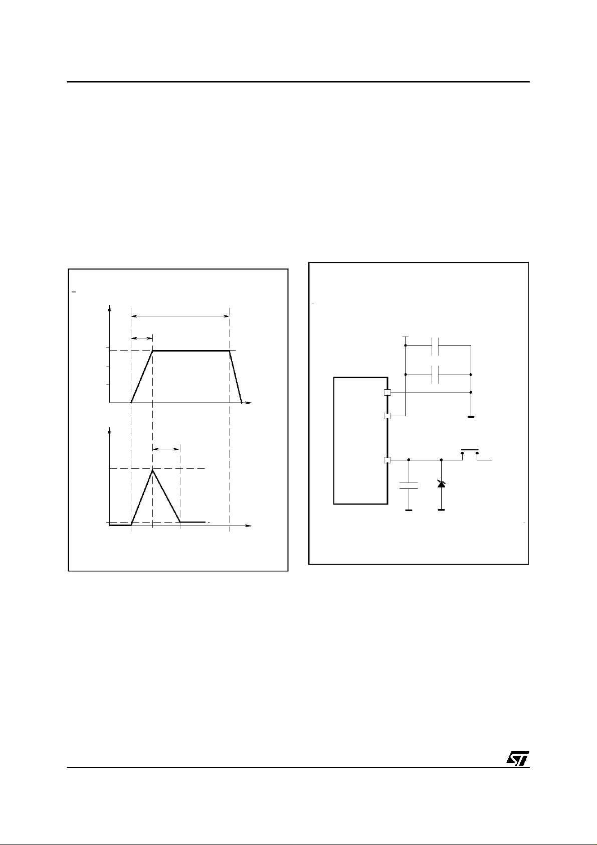
Figure 1. Programming wave form
TEST
100 s max
15
14V typ
10
5
TEST
0.5s min
150 s typ
t
1.2 ROM READOUT PROTECTION
If the ROM READOUT PROTECTION option is
selected, a protection fuse can be blown to prevent any access to the program memory content.
In case the user wants to blow this fuse, high voltage must be applied on the TEST pin.
Figure 2. Programming Circuit
5V
47 F
m
100nF
V
SS
V
DD
PROTECT
100mA
max
4mA typ
t
VR02001
TEST
100nF
ZPD15
15V
14V
VR02003
Note: ZPD15 is used for overvoltage protection
2/10
1
Page 3

ST6200L/01L/03L
ST6200L/01L/03L MICROCONTROLLER OPTION LIST
Customer . . . ..........................
Address .............................
.............................
Contact . . . ..........................
PhoneNo .............................
Reference . . . ..........................
SGS-THOMSON Microelectronics references
Device: [ ] ST6200L [ ] ST6201L [ ] ST6203L
Package: [ ] Dual in Line Plastic[ ] Small Outline Plastic with conditionning:
[ ] Standard (Stick)
[ ] Tape & Reel
Temperature Range: [ ] 0°Cto+70°C
Special Marking: [ ] No [ ] Yes ”_ _ _ _ _ _ _ _ _ _ _ ”
Authorized characters are letters, digits, ’.’, ’-’, ’/’ and spaces only.
Maximum character count: DIP16: 9
SO16: 6
Oscillator Source Selection: [ ] Crystal Quartz/Ceramic resonator
[ ] RC Network
Watchdog Selection: [ ] Software Activation
[ ] Hardware Activation
ROM Readout Protection: [ ] Disabled (Fuse cannot be blown)
[ ] Enabled (Fuse can be blown by the customer)
Note: No part is delivered with protected ROM.
The fuse must be blown for protection to be effective.
External STOP Mode Control[ ] Enabled [ ] Disabled
NMI pin pull-up [ ] Enabled [ ] Disabled
Comments :
Supply Operating Range in the application:
Oscillator Fequency in the application:
Notes . . . ..........................
Signature . . . ..........................
Date .............................
3/10
1
Page 4

ST6200L/01L/03L
1.3 ORDERING INFORMATION
The following section deals with the procedure for
transfer of customer codes to SGS-THOMSON.
1.3.1 Transfer of Customer Code
Customer code is made up of the ROM contents
and the list of the selected mask options. The
ROM contents are to be sent on diskette, or by
electronic means, with the hexadecimal file generated by the development tool. All unused bytes
must be set to FFh.
The selected mask options are communicated to
SGS-THOMSON using the correctly filled OPTION LIST appended.
The SGS-THOMSON Sales Organization will be
pleased to provide detailed information on contractual points.
Table 1. ROM Memory Map for ST6200L,03L
Device Address Description
0000h-0B9Fh
0BA0h-0F9Fh
0FA0h-0FEFh
0FF0h-0FF7h
0FF8h-0FFBh
0FFCh-0FFDh
0FFEh-0FFFh
Reserved
User ROM
Reserved
Interrupt Vectors
Reserved
NMI Interrupt Vector
Reset Vector
1.3.2 Listing Generation and Verification
When SGS-THOMSON receives the user’s ROM
contents, a computer listing is generated from it.
This listing refers exactly to the mask which will be
used to produce the specified MCU. The listing is
then returned to the customer who must thoroughly check, complete, sign and return it to
SGS-THOMSON. The signed listing forms a part
of the contractual agreement for the creation of the
specific customer mask.
Table 2. ROM Memory Map for ST6201L
Device Address Description
0000h-087Fh
0880h-0F9Fh
0FA0h-0FEFh
0FF0h-0FF7h
0FF8h-0FFBh
0FFCh-0FFDh
0FFEh-0FFFh
Reserved
User ROM
Reserved
Interrupt Vectors
Reserved
NMI Interrupt Vector
Reset Vector
Table 3. ROM version Ordering Information
Sales Type ROM Analog inputs Temperature Range Package
ST6200LB1/XXX
ST6200LM1/XXX PSO16
ST6201LB1/XXX
ST6201LM1/XXX PSO16
ST6203LB1/XXX
ST6203LM1/XXX PSO16
1036 Bytes
4
1836 Bytes
1036 Bytes None
0 to +70°C
PDIP16
PDIP16
PDIP16
4/10
1
Page 5

ST6200L/01L/03L
2 ELECTRICAL CHARACTERISTICS
2.1 ABSOLUTE MAXIMUM RATINGS
This product contains devices to protect the inputs
against damage due to high static voltages, however it is advisable to take normal precaution to
avoid application of any voltage higher than the
specified maximum rated voltages.
Power Considerations.The average chip-junction temperature, Tj, in Celsius can be obtained
from:
Tj=TA + PD x RthJA
Where:TA = Ambient Temperature.
For proper operation it is recommended that V
and VObe higher than VSSand lower than VDD.
Reliability is enhanced if unused inputs are connected to an appropriate logic voltage level (V
or VSS).
DD
I
RthJA =Package thermal resistance(junc-
tion-to ambient).
PD = Pint + Pport.
Pint =IDD x VDD (chip internal power).
Pport =Port power dissipation(determined
by the user).
Symbol Parameter Value Unit
V
DD
V
I
V
O
I
O
IV
DD
IV
SS
Tj Junction Temperature 150 °C
T
STG
Notes:
- Stresses above those listed as “absolute maximum ratings” may cause permanent damage to the device. This is a stress ratingonly and
functional operation of the device at these conditions is not implied. Exposure to maximum rating conditions for extended periods may
affect device reliability.
- (1) Withinthese limits,clamping diodes are guarantee to be not conductive. Voltages outside these limits are authorised as longas injection
current is kept withinthe specification.
Supply Voltage -0.3 to 7.0 V
Input Voltage VSS- 0.3 to VDD+ 0.3
Output Voltage VSS- 0.3 to VDD+ 0.3
Current Drain per Pin Excluding VDD,V
TotalCurrent into VDD(source) 50 mA
TotalCurrent out of VSS(sink) 50 mA
Storage Temperature -60 to 150 °C
SS
±10 mA
(1)
(1)
V
V
5/10
1
Page 6

ST6200L/01L/03L
2.2 RECOMMENDED OPERATING CONDITIONS
Symbol Parameter Test Conditions
T
V
f
OSC
I
INJ+
I
Notes:
1. Care mustbe taken in case of negative current injection, where adapted impedance must be respected on analog sources to not affect the
A/D conversion. For a -1mA injection, a maximum 10 KΩ is recommended.
2.An oscillator frequency above 1MHz is recommended for reliable A/D results
Operating Temperature 1 Suffix Version
A
=2MHz
f
Operating Supply Voltage
DD
Oscillator Frequency
2)
OSC
f
=4MHz
OSC
VDD= 2.4V
V
= 3.0V
DD
Pin Injection Current (positive) VDD= 2.4 to 3.9V +5 mA
Pin Injection Current (negative) VDD= 2.4 to 3.9V -5 mA
INJ-
Min. Typ. Max.
070
2.4
3
0
0
Value
3.9
3.9
2.0
4.0
Unit
°C
V
MHz
Figure 3. Maximum Operating FREQUENCY (Fmax) Versus SUPPLY VOLTAGE (VDD)
Maximum FREQUENCY (MHz)
4.0
FUNCTIONALITY IS NOT
GUARANTEED IN
3.5
THIS AREA
3.0
2.5
2.0
1.5
1
0.5
2.1 2.4 2.7 3.3 3.6 3.9
3.0
SUPPLY VOLTAGE (VDD)
The shaded area is outside the recommended operating range; device functionality is not guaranteed under these conditions.
6/10
1
Page 7

ST6200L/01L/03L
2.3 DC ELECTRICAL CHARACTERISTICS
(TA= 0 to +70°C unless otherwise specified)
Symbol Parameter Test Conditions
V
V
V
Hys
V
V
R
I
I
I
DD
Input Low Level Voltage
IL
All Input pins
Input High LevelVoltage
IH
All Input pins
Hysteresis Voltage
All Input pins
Low Level Output Voltage
All Output pins
OL
Low Level Output Voltage
20 mA Sink I/O pins
High Level Output Voltage
OH
All Output pins
Pull-up Resistance
PU
Input Leakage Current
All Input pins but RESET
IL
Input Leakage Current
IH
RESET pin
Supply Current in RESET
Mode
Supply Current in
RUN Mode
Supply Current in WAIT
(3)
Mode
Supply Current in STOP
(3)
Mode
(2)
(1)
= 3V 0.2 V
V
DD
= 3.0V; IOL= +10µA
V
DD
V
= 3.0V; IOL= + 3.0mA
DD
V
= 2.4V; IOL= + 1.5mA
DD
= 3.0V; IOL= +10µA
V
DD
V
= 3.0V; IOL= + 8mA
DD
V
= 3.0V; IOL= +12mA
DD
V
= 2.4V; IOL= + 5mA
DD
= 3.0V; IOH= -10µA
V
DD
V
= 3.0V; IOH= -1.5mA
DD
V
= 2.4V; IOH= -10µA
DD
All Input pins 100 250 600
RESET pin 400 600 1200
VIN=VSS(No Pull-Up configured)
V
IN=VDD
V
IN=VSS
VIN=V
DD
V
RESET=VSS
f
=4MHz
OSC
VDD=3.0V f
VDD=3.0V f
I
=0mA
LOAD
V
=3.0V
DD
=4MHz 1.5 mA
INT
=4MHz 0.5 mA
INT
Value
Min. Typ. Max.
V
DD
V
x 0.8 V
DD
0.1
0.8
0.8
0.1
0.8
1.3
0.8
2.9
2.0
2.3
0.1 1.0
-8 -16 -30
10
1.5 mA
2 µA
Unit
x 0.2 V
V
V
ΚΩ
µA
Notes:
(1) Hysteresis voltage between switching levels
(2) All peripherals running
(3) All peripherals in stand-by
7/10
1
Page 8

ST6200L/01L/03L
DC ELECTRICAL CHARACTERISTICS(Cont’d)
2.4 AC ELECTRICAL CHARACTERISTICS
((TA=0to+70°C unless otherwise specified
Symbol
t
REC
Supply Recovery Time
Parameter Test Conditions
(1)
VDD=3.0V
f
RC
Internal frequency with RC
oscillator
2) 3)
R=47kΩ
R=100kΩ
R=470kΩ
C
C
OUT
Notes:
1. Period for which V
2 An oscillator frequency above 1MHz is recommended for reliable A/D results.
3. Measure performed with OSCin pin soldered on PCB,with an around 2pF equivalent capacitance.
Input Capacitance All Inputs Pins 10 pF
IN
Output Capacitance All Outputs Pins 10 pF
has to be connected at 0V to allow internal Reset function at next power-up.
DD
Value
Min. Typ. Max.
Unit
100 ms
2.5
1.4
450
3
1.7
520
3.5
2.1
600
MHz
MHz
kHz
8/10
1
Page 9

ST6200L/01L/03L
2.5 A/D CONVERTER CHARACTERISTICS
(TA= 0 to +70°C unless otherwise specified)
Symbol Parameter Test Conditions
Min. Typ. Max.
Res Resolution 8 Bit
f
> 1.2MHz, VDD=3.0V
A
TOT
t
C
TotalAccuracy
Conversion Time
(1) (2)
ZIR Zero Input Reading
FSR Full Scale Reading
AD
AC
Notes:
1. Noise at VDD,VSS <10mV
2. With oscillator frequencies less than 1MHz, the A/DConverter accuracy is decreased.
Analog Input Current During
I
Conversion
Analog Input Capacitance 2 5 pF
IN
OSC
f
> 1.2MHz, VDD=2.4V
OSC
f
> 32kHz, VDD=3.0V
OSC
= 2MHz
f
OSC
f
= 4 MHz
OSC
Conversion result when
V
IN=VSS
00 Hex
Conversion result when
V
IN=VDD
V
= 4.0V 1.0 µA
DD
Value
±25
±35
±50
280
140
FF Hex
Unit
mV
µs
2.6 TIMER CHARACTERISTICS
((TA=0to+70°C unless otherwise specified)
Symbol Parameter Test Conditions
f
IN
t
W
Input Frequency on TIMER Pin MHz
Pulse Width at TIMER Pin VDD= 2.4V 250 ns
.
Value
Min. Typ. Max.
Unit
9/10
1
Page 10

ST6200L/01L/03L
Notes:
Information furnished is believed to be accurate and reliable. However, SGS-THOMSON Microelectronics assumes no responsibility for the
consequences of use of such information nor for any infringement of patents or other rights of third parties which may result from its use. No
license is granted by implication or otherwise under any patentor patent rightsof SGS-THOMSON Microelectronics. Specification mentioned
in this publication are subject to change without notice. This publication supersedes and replaces all information previously supplied.
SGS-THOMSON Microelectronics products are not authorized for use as critical components in life support devices or systems without
express written approval of SGS-THOMSON Microelectronics.
1997 SGS-THOMSON Microelectronics -Printed in Italy - All Rights Reserved.
Australia - Brazil - Canada - China - France - Germany - Italy - Japan - Korea - Malaysia - Malta - Morocco - The Netherlands - Singapore
SGS-THOMSON Microelectronics GROUP OF COMPANIES
Spain - Sweden - Switzerland - Taiwan - Thailand - United Kingdom - U.S.A.
10/10
1
 Loading...