

Datasheet ST5R50U, ST5R50MTR, ST5R50M, ST5R33U, ST5R33MTR Datasheet (SGS Thomson Microelectronics)
...Page 1
ST5R00
®
MICROPOWER VFM STEP-UP DC/DC CONVERTER
■
VERY LOW SUPPLY CURRENT
■
REGULATED OUTPUT VOL TA GE
■
WIDE RA NGE OF OUT PU T V O LTA GE
AVAILABLE (2.5V, 2.8V, 3.0V, 3.3V, 5.0V)
■
OUTPUT VOLTAGE ACCURACY ±5%
■
OUTPUT CURRENT UP TO 100mA
■
LOW RIPP LE A ND LOW NOIS E
■
VERY LOW START-UP VOLTAGE
■
HIGH EFFICIENCY (VOUT=5V TYP . 87%)
■
FEW EXTERNAL COMPONENTS
■
VERY SMALL PACKAGE: SOT23-5L, SOT-89
DESCRIPTION
The ST5R00 is an high efficiency VFM Step-up
DC/DC converter for small, low input voltage or
battery powered systems with ult ra low quiescent
supply current. The ST5Rxx accept a positive
input voltage from start-up voltage to V
convert it to a higher output voltage in t he 2.5 to
5V range.
The ST5R00 combine ultra low quiescent supply
current and high efficiency to give maximum
battery life. The high switching frequency and
the internally limited peak inductor current,
permits the use of small, low cost inductors. Only
three external components are nedeed: an
inductor a diode and an output capacitor.
OUT
and
SERIES
SOT23-5L
The ST5R00 is suitable to be used in a battery
powered equipment where low noise, low ripple
and ultra low supply current are required. The
ST5R00 is available in very small packages:
SOT23-5L, SOT-89.
Typical applications are pagers, cameras &
video camera, cellular telephones, wireless
telephones, palmtop computer, battery backup
supplies, battery powered equipment.
SOT-89
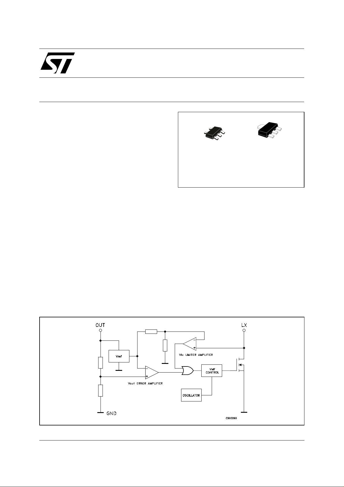
SCHEMATIC DIAGRAM
June 2001
1/13
Page 2
ST5R00
ABSOLUTE MAXIMUM RATING
Symbol Parameter Value Unit
V
(*) Reduced by 1.7 mW for increasing in TA of 1oC over 25oC
THERMAL DATA
Symbol Parameter SOT23-5L SOT-89 Unit
R
thj-case
Output Voltage 5.5 V
OUT
Input Voltage 5.5 V
V
IN
V
LX Pin Voltage 5.5 V
LX
LX Pin Output Current Internally limited
I
LX
P
Power Dissipation @ 25oC fo r S OT2 3-5L 170 (*) mW
tot
Storage Temperature Range - 55 to 125
T
stg
Operating Junction Temperature Range - 2 5 to 8 5
T
op
Therma l Resistance Junction-case 63 17 °C/W
o
C
o
C
OPERATION
The ST5Rxx architecture is built around a VFM
CONTROL logic core: switching frequency is set
through a built in oscillator: T
5µs) while T
time is determined by the error
OFF
time is fixed (Typ.
ON
amplifier output, a logic signal coming from the
comparison made by the Error Amplifier Stage
between the signal coming from the output
voltage divider network and the internal
Band-Gap voltage reference (V
ref
). T
reaches
OFF
a minimum (Typ. 1.7µs) when heavy load
conditions are met (Clock frequency 150KHz). An
over current conditions, through the internal
power switch, causes a voltage drop
V
LX=RDSONxISW
the internal switch to be off, so narrowing T
and the VLX limiter block forces
ON
case the switching frequency may be higher than
the 150KHz set by the internal clock generator.
VFM control ensures very low quiescent current
and high conversion efficiency even with very
light loads.
Since the Output Voltage pin is also used as the
device Supply Voltage, the versions with higher
output voltage present an higher internal supply
voltage that results in lower power switch R
slightly greater output power and higher
efficiency. Moreover, bootstrapping allows the
input voltage to sag to 0.6V (at I
the system is started.
If the input voltage exceeds the output voltage,
the output will follow the input, however, the input
or output voltage must not be forced above 5.5V.
time and limiting internal power dissipation. In this
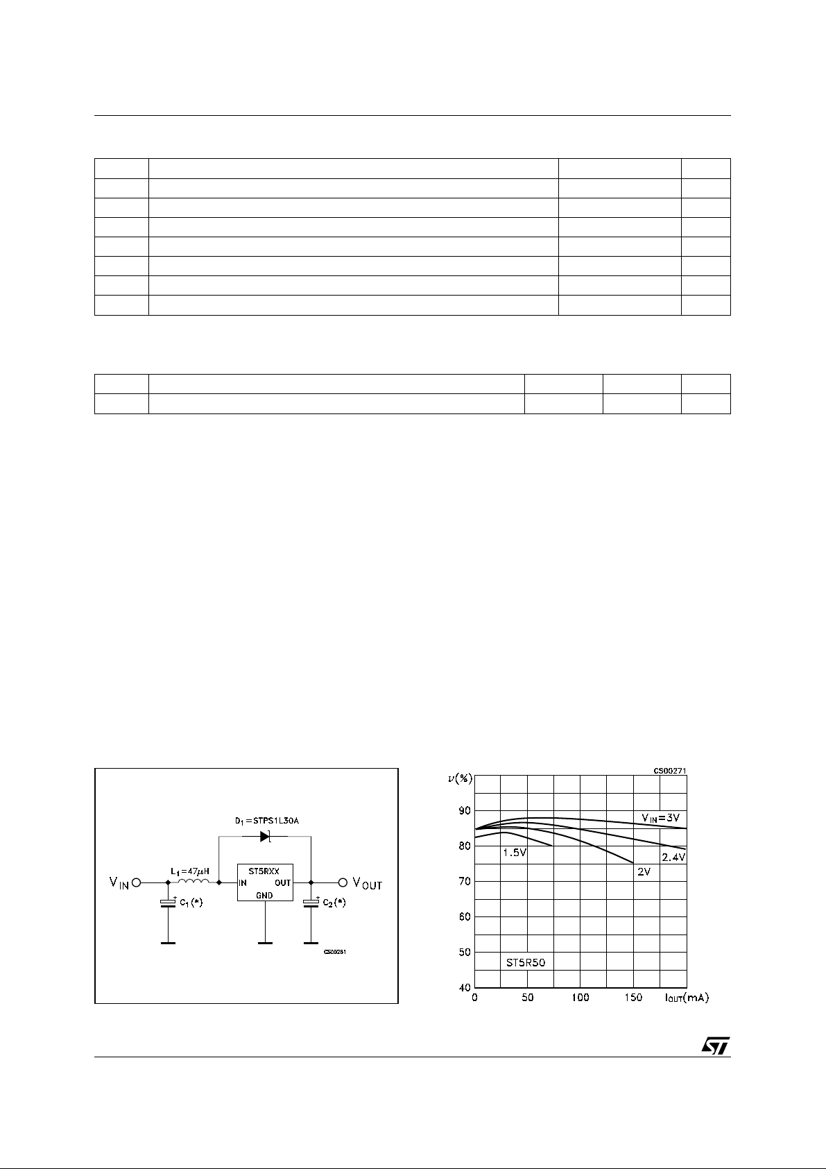
Typical Application Circuit Typical Application Efficency
=1mA) once
OUT
DSON
,
(*) See application info
2/13
Page 3
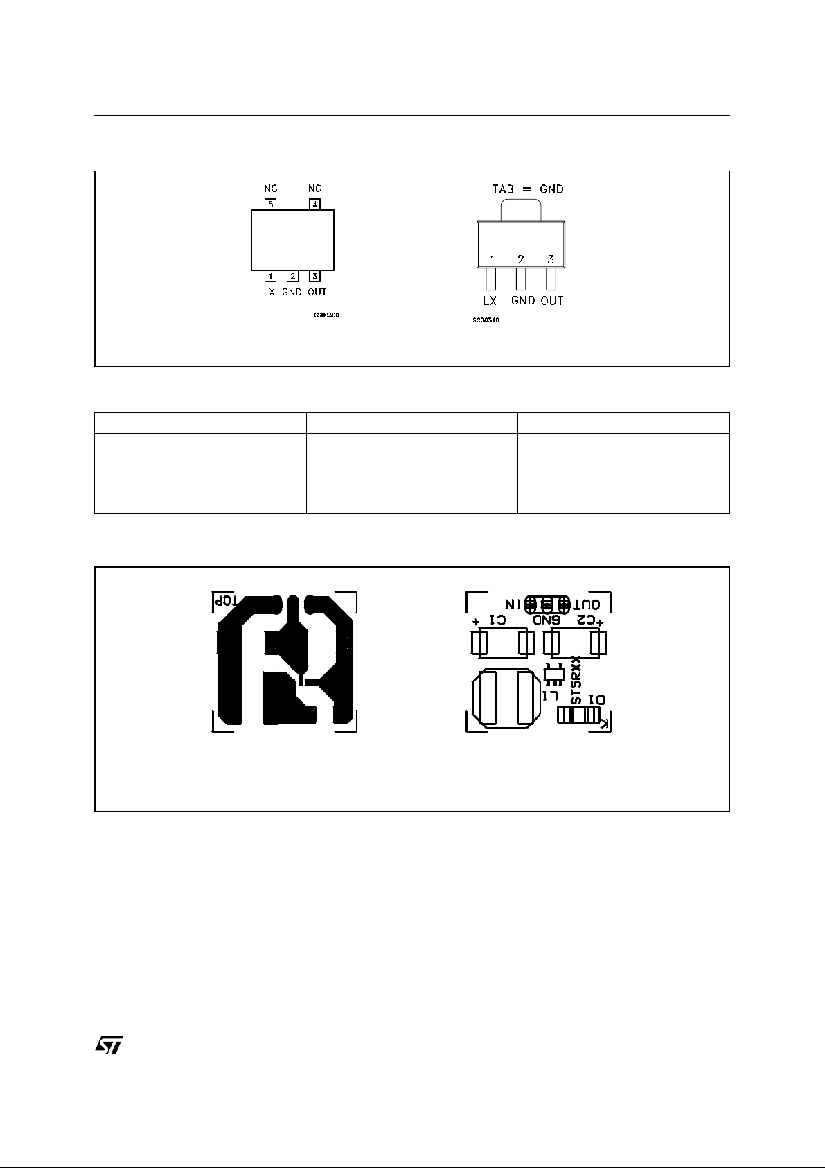
CONNECTION DIAGRAM (top view)
SOT23-5L SOT-89
ORDERING NUMBERS
SOT23-5L SOT-89 Output Voltage
ST5R25M
ST5R28M
ST5R30M
ST5R33M
ST5R50M
ST5R25U
ST5R28U
ST5R30U
ST5R33U
ST5R50U
ST5R00
2.5 V
2.8 V
3.0 V
3.3 V
5.0 V
TYPICAL DEMOBOARD
3/13
Page 4
ST5R00
ELECTRICAL CHARACTERISTICS FOR ST5R25
(V
= 1.5V, I
IN
otherwise notes, refer to the typical operating circuit.
Symbol Parameter Test Conditions Min. Typ. Max. Unit
V
OUT
V
START-UP
V
HOLD
I
SUPPLY
R
LX(DSON)
I
LX(leak)
F
osc
Dty Oscillator Duty Cycle to be measure on Lx pin 77 %
ν
(1): The minimum input voltage for the IC start-up is strictly a function of the VF catch diode.
ELECTRICAL CHARACTERISTICS FOR ST5R28
= 1.7V, I
(V
IN
otherwise notes, refer to the typical operating circuit.
Symbol Parameter Test Conditions Min. Typ. Max. Unit
V
OUT
V
START-UP
V
HOLD
I
SUPPLY
R
LX(DSON)
I
LX(leak)
F
osc
Dty Oscillator Duty Cycle to be measure on Lx pin 77 %
ν
(1): The minimum input voltage for the IC start-up is strictly a function of the VF catch diode.
= 10mA TA = 25oC unless otherwise specified. For external components value, unless
OUT
Output Voltage 2.375 2.5 2.625 V
Start-up Voltage (VIN-VF) (1) I
Hold-on Voltage I
=1mA VIN rising from 0 to 2V 0.8 1.2 V
OUT
=1mA VIN falling from 2 to 0V 0.6 V
OUT
Supply Current To be measured at VIN, no load 16
Internal Switch R
DSON
Internal Leakage Current VLX=4V, forced V
ILX=150mA 850 m
=3V 0.5
OUT
Maximum oscillator Frequency 150 kHz
Efficency I
= 10mA TA = 25oC unless otherwise specified. For external components value, unless
OUT
=50mA 82 %
OUT
Output Voltage 2.66 2.8 2.94 V
Start-up Voltage (VIN-VF) (1) I
Hold-on Voltage I
=1mA VIN rising from 0 to 2V 0.8 1.2 V
OUT
=1mA VIN falling from 2 to 0V 0.6 V
OUT
Supply Current To be measured at VIN, no load 16
Internal Switch R
DSON
Internal Leakage Current VLX=4V, forced V
ILX=150mA 850 m
=3.3V 0.5
OUT
Maximum oscillator Frequency 150 kHz
Efficency I
=50mA 82 %
OUT
A
µ
Ω
A
µ
A
µ
Ω
A
µ
ELECTRICAL CHARACTERISTICS FOR ST5R30
(V
IN
= 1.8V, I
= 10mA TA = 25oC unless otherwise specified. For external components value, unless
OUT
otherwise notes, refer to the typical operating circuit.
Symbol Parameter Test Conditions Min. Typ. Max. Unit
V
OUT
V
START-UP
V
HOLD
I
SUPPLY
R
LX(DSON)
I
LX(leak)
F
Dty Oscillator Duty Cycle to be measure on Lx pin 77 %
(1): The minimum input voltage for the IC start-up is strictly a function of the VF catch diode.
4/13
Output Voltage 2.85 3 3.15 V
Start-up Voltage (VIN-VF) (1) I
Hold-on Voltage I
=1mA VIN rising from 0 to 2V 0.8 1.2 V
OUT
=1mA VIN falling from 2 to 0V 0.6 V
OUT
Supply Current To be measured at VIN, no load 17
Internal Switch R
DSON
Internal Leakage Current VLX=4V, forced V
Maximum oscillator Frequency 150 kHz
osc
Efficency I
ν
ILX=150mA 850 m
=3.5V 0.5
OUT
=50mA 83 %
OUT
A
µ
Ω
A
µ
Page 5

ST5R00
ELECTRICAL CHARACTERISTICS FOR ST5R33
(V
= 2V, I
IN
otherwise notes, refer to the typical operating circuit.
Symbol Parameter Test Conditions Min. Typ. Max. Unit
V
OUT
V
START-UP
V
HOLD
I
SUPPLY
R
LX(DSON)
I
LX(leak)
F
osc
Dty Oscillator Duty Cycle to be measure on Lx pin 77 %
ν
(1): The minimum input voltage for the IC start-up is strictly a function of the VF catch diode.
ELECTRICAL CHARACTERISTICS FOR ST5R50
= 3V, I
(V
IN
otherwise notes, refer to the typical operating circuit.
Symbol Parameter Test Conditions Min. Typ. Max. Unit
V
OUT
V
START-UP
V
HOLD
I
SUPPLY
R
LX(DSON)
I
LX(leak)
F
osc
Dty Oscillator Duty Cycle to be measure on Lx pin 77 %
ν
(1): The minimum input voltage for the IC start-up is strictly a function of the VF catch diode.
= 10mA TA = 25oC unless otherwise specified. For external components value, unless
OUT
Output Voltage 3.135 3.3 3.465 V
Start-up Voltage (VIN-VF) (1) I
Hold-on Voltage I
=1mA VIN rising from 0 to 2V 0.8 1.2 V
OUT
=1mA VIN falling from 2 to 0V 0.6 V
OUT
Supply Current To be measured at VIN, no load 17
Internal Switch R
DSON
Internal Leakage Current VLX=4V, forced V
ILX=150mA 850 m
=3.8V 0.5
OUT
Maximum oscillator Frequency 150 kHz
Efficency I
= 10mA TA = 25oC unless otherwise specified. For external components value, unless
OUT
=50mA 83 %
OUT
Output Voltage 4.75 5.0 5.25 V
Start-up Voltage (VIN-VF) (1) I
Hold-on Voltage I
=1mA VIN rising from 0 to 2V 0.8 1.2 V
OUT
=1mA VIN falling from 2 to 0V 0.6 V
OUT
Supply Current To be measured at VIN, no load 18
Internal Switch R
DSON
Internal Leakage Current VLX=4V, forced V
ILX=150mA 700 m
=5.5V 0.5
OUT
Maximum oscillator Frequency 160 kHz
Efficency I
=50mA 87 %
OUT
A
µ
Ω
A
µ
A
µ
Ω
A
µ
TYPICAL OPERATING CHARACTERISTICS (the following plots are referred to the typical application
circuit and, unless otherwise noted, at T
=25oC)
A
Figure 1:Output Voltage vs Output Current Figure 2: Output Voltage vs Output Current
5/13
Page 6

ST5R00
Figure 3: Output Voltage vs Temperature Figure 4: Output Voltage vs Temperature
Figure 5: Efficency vs Temperature Figure 6: Efficency vs Temperature
Figure 7: Efficency vs Output Current Figure 8: Efficency vs Output Current
6/13
Page 7

ST5R00
Figure 9: Maximum Oscillator Frequency vs
Temperature
Figure 11: Oscillator Duty Cycle (@ MAX Freq.)
vs Temperature
Figure 10: Maximum Oscillator Frequency vs
Temperature
Figure 12: Oscillator Duty Cycle (@ MAX Freq.)
vs Temperature
Figure 13: Lx Switching Current Limit vs
Temperature
Figure 14: Lx Switching Current Limit vs
Temperature
7/13
Page 8

ST5R00
Figure 15: Start-up Voltage (V
IN-VF
) vs
Temperature
(*) Input Voltage less the voltage drop across the diode (*) Input Voltage less the voltage drop across the diode
Figure 17: Start-up Voltage (V
IN-VF
) vs Output
Current
Figure 16: Start-up Voltage (V
Temperature
Figure 18: Start-up Voltage (V
Current
IN-VF
IN-VF
) vs
) vs Output
(*) Input Voltage less the voltage drop across the diode (*) Input Voltage less the voltage drop across the diode
Figure 19: Minimum Input Voltage vs Output
Current
8/13
Figure 20: Minimum Input Voltage vs Output
Current
Page 9

ST5R00
Figure 21: Internal Switch R
vs Temperature
DSON
Figure 22: Internal Switch R
vs Temperature
DSON
Figure 23: Hold-on Voltage vs Temperature Figure 24: Hold-on Voltage vs Temperature
Figure 25: No Load Input Current vs
Temperature
Figure 26: No Load Input Current vs
Temperature
9/13
Page 10

ST5R00
APPLICATION INFORMATION
PC LAYOUT AND GROUNDING HINTS
The ST5R00 high frequency operation makes PC
layout important for minimizing ground bounce
and noise. Place external components as close
as possible to the device pins. Take care to the
Supply Voltage Source connections that have to
be very close to the Input of the application. Set
the Output Load as close as possible to the
output capacitor. If possible, use a Star ground
connection with the centre point on the Device
Ground pin. To maximize output power and
efficiency and minimize output ripple voltage, us e
a ground plane and solder the ICs ground pin
directly to the ground plane.
Remember that the LX Switching Current flows
through the Ground pin, so, in order to minimize
the series resistance that may cause power
dissipation and decrease of the Efficiency
conversion, the Ground pattern has to be as large
as possible.
INDUCTOR SELECTION
An inductor value of 47µH performs well in most
ST5R00 applications. However, the inductance
value is not critical, and the ST5R00 will work
with inductors in the 33µH to 120µH. Smaller
inductance values typically offer a smaller
physical size for a given series resistance,
allowing the smallest overall circuit dimensions.
However, due to higher peak inductor currents,
the output voltage ripple (Ipeak x output filter
capacitors ESR) also tends to be higher. Circuits
using larger inductance values exhibit higher
output current capability and larger physical
dimensions for a given series resistance.
In order to obtain the best application
performances the inductor must respect the
following condition:
- The DC resistance has to be as little as
possible, a good value is <0.25Ω. This choise will
reduce the lost power as heat in the windings.
- The inductor core must not saturate at the
forecast maximum LX current. This is mainly a
function of the Input Voltage, Inductor value and
Output Current. However, it is generally
accettable to bias the inductor into saturation by
as much as 20%, although this will slightly reduce
efficiency. In order to calculate this parameter we
have to distinguish two cases:
1)When a light load is applied on the output
(discontinuous mode operation) the inductor core
must not saturate at
I
= (VIN x TON)/L.
LX(max)
2)For heavy load (continuos mode operation) t he
inductor core must not saturate at
I
LX(max)
= (I
OUT
x T)/T
OFF(min)
+ (VIN x TON)/2L
Where: Vin is the Input Voltage, Ton is the switch
on period (typ. 5µs), L is the inductance value,
Iout is the maximum forecast
Output Current, T=T
ON+TOFF(min)
and T
OFF(min)
is
the minimum switch off period (typ. 1.7µs),
- Choose an inductance value in the 47µH to
82µH range.
- For application sensitive to Electromagnetic
Interference (EMI), a pot core inductor is
recommended.
DIODE SELECTION
A Schottky diode with an high switching speed
and a very low Forward Voltage (V
Higher V
may cause lost power as heat in the
F
) is needed.
F
diode, with a decrease of the Efficiency.
Moreover, since the Output Voltage pin is also
used as the device Supply Voltage, the Start-up
Voltage (see related plots) is strictly due to the
diode Forward Voltage at the rated Forward
Current. A good diode choise is a STPS1L30A
(STM).
INPUT/OUTPUT CAPACITORS SELECTION
The Output Ripple Voltage, as well as the
Efficiency, is strictly related to the behaviour of
these elements. The output ripple voltage is the
product of the peak inductor current and the
output capacitor Equivalent Series Resistance
(ESR). Best performances are obtained with
good high frequency characteristics capacitors
and low ESR. The best compromise for the value
of the Output Capacitance is 47µF Tantalum
Capacitor, Lower values may cause higher
Output Ripple Voltage and lower Efficiency
without compromising the functionality of the
device.
An Input Capacitor is required to compensate, if
present, the series impedance between the
Supply Voltage Source and the Input Voltage of
the Application.
A value of 4.7µF is enough to guarantee stability
for distances less than 2". It could be nec essary
(depending on V
IN
, V
OUT
, I
values) to
OUT
proportionally increase the input capacitor value
up to 100µA for major distances.
In any case we suggest to connect both
capacitors, C
and C
IN
, as close as possible to
OUT
the device pins.
10/13
Page 11

SOT-89 MECHANICAL DATA
ST5R00
DIM.
MIN. TYP. MAX. MIN. TYP. MAX.
A 1.4 1.6 55.1 63.0
B 0.44 0.56 17.3 22.0
B1 0.36 0.48 14.2 18.9
C 0.35 0.44 13.8 17.3
C1 0.35 0.44 13.8 17.3
D 4.4 4.6 173.2 181.1
D1 1.62 1.83 63.8 72.0
E 2.29 2.6 90.2 102.4
e 1.42 1.57 55.9 61.8
e1 2.92 3.07 115.0 120.9
H 3.94 4.25 155.1 167.3
L 0.89 1.2 35.0 47.2
mm mils
P025H
11/13
Page 12

ST5R00
SOT23-5L MECHANICAL DATA
DIM.
MIN. TYP. MAX. MIN. TYP. MAX.
A 0.90 1.45 35.4 57.1
A1 0.00 0.15 0.0 5.9
A2 0.90 1.30 35.4 51.2
b 0.35 0.50 13.7 19.7
C 0.09 0.20 3.5 7.8
D 2.80 3.00 110.2 118.1
E 2.60 3.00 102.3 118.1
E1 1.50 1.75 59.0 68.8
L 0.35 0.55 13.7 21.6
e 0.95 37.4
e1 1.9 74.8
mm mils
12/13
Page 13

ST5R00
Information furnished is believed to be accurate and reliable. However, STMicroelectronics assumes no responsibility for the consequences
of use of suc h infor mation nor for any i nfringement of patents or other r ights of thir d partie s which may resul t from i ts use. No license is
granted by implication or otherwise under any patent or patent rights of STMicroelectronics. Specification mentioned in this publication are
subject to change without notice. This publication supersedes and replaces all information previously supplied. STMicroelectronics products
are not authorized for use as critical components in life support devices or systems without express written approval of STMicr oelectronics.
The ST logo is a registered trademark of STMicroelectronics
© 2001 STMicroelectronics – Print ed in Italy – All Rights Reserved
STMicroelectronics GROUP OF COMPANIES
Australia - Brazil - China - Finland - France - Germany - Hong Kong - India - I taly - Japan - Malaysia - Malta - Morocco
Singapore - Spain - Sweden - Switzerland - United King dom - U .S. A.
http://www.st.com
.
13/13
 Loading...