

Page 1

®
ST52T430/E430
8-BIT INTELLIGENT CONTROLLER UNIT (ICU)
Memories
Up to 8 Kbytes EPROM/OTP
256 bytes of RAM
Readout Protection
Core
Register File Based Architecture
55 instru ctio ns
Hardware multiplication and division
Decision Processor for the implementation of
Fuzzy Logic algorithms
Clock and Power Supply
Up to 20 MHz clock frequency.
Power Saving features
Interrupts
6 interrupt vectors
Top Level External Interrupt (INT)
ST52T430/E43 0
Three Timer/PWMs, ADC, SCI
PRELIMINARY DATA SHE ET
Peripherals
3 Programmable 8-bit Timer/PWMs with internal
16-bit Prescaler featuring:
– PWM output
– Input capture
– Output Compare
– Pulse Generator mode
Watchdog timer
On-chip 8-bit Sample and Hold A/D Converter
with 8-channel analog multiplexer
Serial Communication Interface with
asynchronous protocol (UART)
I/O Ports
23 I/O PINs configurable in Input and Output
mode
High current sink/source in all pins.
Development tools
High level Software tools
Emulator
Low cost Programmer
Gang Programmer
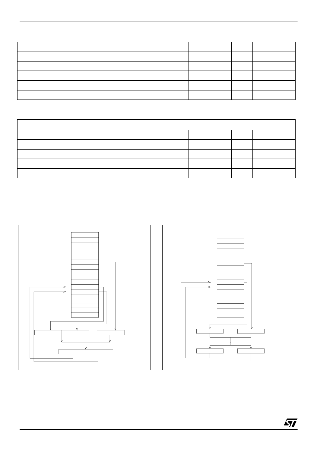
ST52x430 Devices Summary
Device NVM RAM
ST52T430K1 2K OTP 256 3x8-bit 8-Ch Yes Yes 3.0-5.5 V 23 Sdip32 Sso34 Tqfp32
ST52T430K2 4K OTP 256 3x8-bit 8-Ch Yes Yes 3.0-5.5 V 23 Sdip32 Sso34 Tqfp32
ST52T430K3 8K OTP 256 3x8-bit 8-Ch Yes Yes 3.0-5.5 V 23 Sdip32 Sso34 Tqfp32
ST52E430K3 8K EPROM 256 3x8-bit 8-Ch Yes Yes 3.0-5.5 V 23 Csdip32w
Timer
PWM
ADC SCI Watchdog
Operating
Supply
I/O Package
Rev. 1.9 - May 2003 1/88
This is preliminary information on a new product foreseen to be developed. Details are subject to change without notice.
Page 2

ST52T430/E430
2/88
Page 3

ST52T430/E430
TABLE OF CONTENTS
TABLE OF CONTENTS
1 GENERAL DESCRIP TION. . . . . . . . . . . . . . . . . . . . . . . . . . . . . . . . . . . . . . . . . 7
1.1 Introduction. . . . . . . . . . . . . . . . . . . . . . . . . . . . . . . . . . . . . . . . . . . . . . . . . . . . . . . . . . . . . . . . . . .7
1.2 Functional Description . . . . . . . . . . . . . . . . . . . . . . . . . . . . . . . . . . . . . . . . . . . . . . . . . . . . . . . . . .7
1.2.1 Memory Programming Mode . . . . . . . . . . . . . . . . . . . . . . . . . . . . . . . . . . . . . . . . . . . . . . . . 7
1.2.2 Working mode. . . . . . . . . . . . . . . . . . . . . . . . . . . . . . . . . . . . . . . . . . . . . . . . . . . . . . . . . . . . 8
1.3 Pin Description . . . . . . . . . . . . . . . . . . . . . . . . . . . . . . . . . . . . . . . . . . . . . . . . . . . . . . . . . . . . . . .12
2 INTER NAL ARCHI T ECTURE. . . . . . . . . . . . . . . . . . . . . . . . . . . . . . . . . . . . . . 14
2.1 ST52x430 Operating Modes. . . . . . . . . . . . . . . . . . . . . . . . . . . . . . . . . . . . . . . . . . . . . . . . . . . . .14
2.2 Control Unit and Data Processing Unit. . . . . . . . . . . . . . . . . . . . . . . . . . . . . . . . . . . . . . . . . . . . .14
2.2.1 Program Counter . . . . . . . . . . . . . . . . . . . . . . . . . . . . . . . . . . . . . . . . . . . . . . . . . . . . . . . . 14
2.2.2 Flags. . . . . . . . . . . . . . . . . . . . . . . . . . . . . . . . . . . . . . . . . . . . . . . . . . . . . . . . . . . . . . . . . . 14
2.3 Address Spaces . . . . . . . . . . . . . . . . . . . . . . . . . . . . . . . . . . . . . . . . . . . . . . . . . . . . . . . . . . . . . .16
2.3.1 RAM and STACK . . . . . . . . . . . . . . . . . . . . . . . . . . . . . . . . . . . . . . . . . . . . . . . . . . . . . . . . 16
2.3.2 Input Registers Bench . . . . . . . . . . . . . . . . . . . . . . . . . . . . . . . . . . . . . . . . . . . . . . . . . . . . 17
2.3.3 Configuration Registers . . . . . . . . . . . . . . . . . . . . . . . . . . . . . . . . . . . . . . . . . . . . . . . . . . . 18
2.3.4 Output Registers. . . . . . . . . . . . . . . . . . . . . . . . . . . . . . . . . . . . . . . . . . . . . . . . . . . . . . . . . 19
2.4 Arithmetic Logic Unit. . . . . . . . . . . . . . . . . . . . . . . . . . . . . . . . . . . . . . . . . . . . . . . . . . . . . . . . . . .20
3 EPROM. . . . . . . . . . . . . . . . . . . . . . . . . . . . . . . . . . . . . . . . . . . . . . . . . . . . . . . 23
3.1 EPROM Programming Phase Procedure . . . . . . . . . . . . . . . . . . . . . . . . . . . . . . . . . . . . . . . . . . .24
3.1.1 EPROM Operation . . . . . . . . . . . . . . . . . . . . . . . . . . . . . . . . . . . . . . . . . . . . . . . . . . . . . . . 25
3.1.2 EPROM Locking. . . . . . . . . . . . . . . . . . . . . . . . . . . . . . . . . . . . . . . . . . . . . . . . . . . . . . . . . 25
3.1.3 EPROM Writing . . . . . . . . . . . . . . . . . . . . . . . . . . . . . . . . . . . . . . . . . . . . . . . . . . . . . . . . . 2 5
3.1.4 EPROM Read/Verify Margin Mode. . . . . . . . . . . . . . . . . . . . . . . . . . . . . . . . . . . . . . . . . . . 26
3.1.5 Stand by Mode . . . . . . . . . . . . . . . . . . . . . . . . . . . . . . . . . . . . . . . . . . . . . . . . . . . . . . . . . . 2 6
3.1.6 ID code . . . . . . . . . . . . . . . . . . . . . . . . . . . . . . . . . . . . . . . . . . . . . . . . . . . . . . . . . . . . . . . . 26
3.2 Eprom Erasure . . . . . . . . . . . . . . . . . . . . . . . . . . . . . . . . . . . . . . . . . . . . . . . . . . . . . . . . . . . . . . .26
4 INTER RUPTS . . . . . . . . . . . . . . . . . . . . . . . . . . . . . . . . . . . . . . . . . . . . . . . . . . 27
4.1 Interrupt Operation . . . . . . . . . . . . . . . . . . . . . . . . . . . . . . . . . . . . . . . . . . . . . . . . . . . . . . . . . . . .27
4.2 Global Interrupt Request Enabling . . . . . . . . . . . . . . . . . . . . . . . . . . . . . . . . . . . . . . . . . . . . . . . .27
4.3 Interrupt Sources . . . . . . . . . . . . . . . . . . . . . . . . . . . . . . . . . . . . . . . . . . . . . . . . . . . . . . . . . . . . .28
4.4 Interru p t M as kability . . . . . . . . . . . . . . . . . . . . . . . . . . . . . . . . . . . . . . . . . . . . . . . . . . . . . . . . . . .28
4.5 Interrupt Priority . . . . . . . . . . . . . . . . . . . . . . . . . . . . . . . . . . . . . . . . . . . . . . . . . . . . . . . . . . . . . .30
4.6 Interrupts and Low power mode . . . . . . . . . . . . . . . . . . . . . . . . . . . . . . . . . . . . . . . . . . . . . . . . . . 3 1
4.7 Interrupt RESET . . . . . . . . . . . . . . . . . . . . . . . . . . . . . . . . . . . . . . . . . . . . . . . . . . . . . . . . . . . . . .31
5 CLOCK, RESET & POWER SAVING MODE. . . . . . . . . . . . . . . . . . . . . . . . . . 32
5.1 System Clock . . . . . . . . . . . . . . . . . . . . . . . . . . . . . . . . . . . . . . . . . . . . . . . . . . . . . . . . . . . . . . . .32
5.2 RESET . . . . . . . . . . . . . . . . . . . . . . . . . . . . . . . . . . . . . . . . . . . . . . . . . . . . . . . . . . . . . . . . . . . . .3 2
5.3 Power Saving Mode . . . . . . . . . . . . . . . . . . . . . . . . . . . . . . . . . . . . . . . . . . . . . . . . . . . . . . . . . . .32
5.3.1 Wait Mode. . . . . . . . . . . . . . . . . . . . . . . . . . . . . . . . . . . . . . . . . . . . . . . . . . . . . . . . . . . . . . 32
5.3.2 Halt Mode . . . . . . . . . . . . . . . . . . . . . . . . . . . . . . . . . . . . . . . . . . . . . . . . . . . . . . . . . . . . . . 33
3/88
Page 4

ST52T430/E430
6 I/O PORTS . . . . . . . . . . . . . . . . . . . . . . . . . . . . . . . . . . . . . . . . . . . . . . . . . . . . 35
6.1 Introduction. . . . . . . . . . . . . . . . . . . . . . . . . . . . . . . . . . . . . . . . . . . . . . . . . . . . . . . . . . . . . . . . . .3 5
6.2 Input Mode . . . . . . . . . . . . . . . . . . . . . . . . . . . . . . . . . . . . . . . . . . . . . . . . . . . . . . . . . . . . . . . . . . 3 5
6.3 Output Mode. . . . . . . . . . . . . . . . . . . . . . . . . . . . . . . . . . . . . . . . . . . . . . . . . . . . . . . . . . . . . . . . . 3 6
6.4 Alternate Functions. . . . . . . . . . . . . . . . . . . . . . . . . . . . . . . . . . . . . . . . . . . . . . . . . . . . . . . . . . . .36
6.5 I/O Port Configuration Registers . . . . . . . . . . . . . . . . . . . . . . . . . . . . . . . . . . . . . . . . . . . . . . . . . .36
7 FUZZY COMPUTA T ION (DP). . . . . . . . . . . . . . . . . . . . . . . . . . . . . . . . . . . . . . 41
7.1 Fuzzy Inference . . . . . . . . . . . . . . . . . . . . . . . . . . . . . . . . . . . . . . . . . . . . . . . . . . . . . . . . . . . . . .41
7.2 Fuzzyfication Phase . . . . . . . . . . . . . . . . . . . . . . . . . . . . . . . . . . . . . . . . . . . . . . . . . . . . . . . . . . .41
7.3 Inference Phase . . . . . . . . . . . . . . . . . . . . . . . . . . . . . . . . . . . . . . . . . . . . . . . . . . . . . . . . . . . . . .41
7.4 Defuzzyfication . . . . . . . . . . . . . . . . . . . . . . . . . . . . . . . . . . . . . . . . . . . . . . . . . . . . . . . . . . . . . . .42
7.5 Input Membership Function . . . . . . . . . . . . . . . . . . . . . . . . . . . . . . . . . . . . . . . . . . . . . . . . . . . . .42
7.6 Output Singleton. . . . . . . . . . . . . . . . . . . . . . . . . . . . . . . . . . . . . . . . . . . . . . . . . . . . . . . . . . . . . .43
7.7 Fuzzy Rules . . . . . . . . . . . . . . . . . . . . . . . . . . . . . . . . . . . . . . . . . . . . . . . . . . . . . . . . . . . . . . . . .43
8 A/D CONVERTER. . . . . . . . . . . . . . . . . . . . . . . . . . . . . . . . . . . . . . . . . . . . . . . 45
8.1 Introduction. . . . . . . . . . . . . . . . . . . . . . . . . . . . . . . . . . . . . . . . . . . . . . . . . . . . . . . . . . . . . . . . . .4 5
8.2 Operational Description . . . . . . . . . . . . . . . . . . . . . . . . . . . . . . . . . . . . . . . . . . . . . . . . . . . . . . . .45
8.2.1 Operating Modes . . . . . . . . . . . . . . . . . . . . . . . . . . . . . . . . . . . . . . . . . . . . . . . . . . . . . . . . 46
8.2.2 Power Down Mode . . . . . . . . . . . . . . . . . . . . . . . . . . . . . . . . . . . . . . . . . . . . . . . . . . . . . . . 47
8.3 A/D Registers Description. . . . . . . . . . . . . . . . . . . . . . . . . . . . . . . . . . . . . . . . . . . . . . . . . . . . . . .47
9 WATCHDOG TIMER. . . . . . . . . . . . . . . . . . . . . . . . . . . . . . . . . . . . . . . . . . . . . 48
9.1 Operational Description . . . . . . . . . . . . . . . . . . . . . . . . . . . . . . . . . . . . . . . . . . . . . . . . . . . . . . . .48
9.2 Register Description . . . . . . . . . . . . . . . . . . . . . . . . . . . . . . . . . . . . . . . . . . . . . . . . . . . . . . . . . . .49
10 PWM/TIMER . . . . . . . . . . . . . . . . . . . . . . . . . . . . . . . . . . . . . . . . . . . . . . . . . . 50
10.1 Timer Mode. . . . . . . . . . . . . . . . . . . . . . . . . . . . . . . . . . . . . . . . . . . . . . . . . . . . . . . . . . . . . . . . .50
10.2 PWM Mode. . . . . . . . . . . . . . . . . . . . . . . . . . . . . . . . . . . . . . . . . . . . . . . . . . . . . . . . . . . . . . . . .52
10.3 Timer Interrupt . . . . . . . . . . . . . . . . . . . . . . . . . . . . . . . . . . . . . . . . . . . . . . . . . . . . . . . . . . . . . .5 3
11 SERI AL COMMUNIC AT ION INTE RF ACE. . . . . . . . . . . . . . . . . . . . . . . . . . . 64
11.1 SCI Receiver block . . . . . . . . . . . . . . . . . . . . . . . . . . . . . . . . . . . . . . . . . . . . . . . . . . . . . . . . . . .6 4
11.2 SCI Transmitter Block. . . . . . . . . . . . . . . . . . . . . . . . . . . . . . . . . . . . . . . . . . . . . . . . . . . . . . . . .66
11.3 Baud Rate Generator Block . . . . . . . . . . . . . . . . . . . . . . . . . . . . . . . . . . . . . . . . . . . . . . . . . . . .67
12 ELECTRICAL CH ARACTERIS TICS . . . . . . . . . . . . . . . . . . . . . . . . . . . . . . . 68
12.1 Parameter Conditions. . . . . . . . . . . . . . . . . . . . . . . . . . . . . . . . . . . . . . . . . . . . . . . . . . . . . . . . .68
12.1.1 Minimum and Maximum values . . . . . . . . . . . . . . . . . . . . . . . . . . . . . . . . . . . . . . . . . . . . 68
12.1.2 Typical values. . . . . . . . . . . . . . . . . . . . . . . . . . . . . . . . . . . . . . . . . . . . . . . . . . . . . . . . . . 68
12.1.3 Typical curves. . . . . . . . . . . . . . . . . . . . . . . . . . . . . . . . . . . . . . . . . . . . . . . . . . . . . . . . . . 6 8
12.1.4 Loading capacitor . . . . . . . . . . . . . . . . . . . . . . . . . . . . . . . . . . . . . . . . . . . . . . . . . . . . . . . 68
12.1.5 Pin input voltage. . . . . . . . . . . . . . . . . . . . . . . . . . . . . . . . . . . . . . . . . . . . . . . . . . . . . . . . 68
12.2 Absolute Maximum Ratings . . . . . . . . . . . . . . . . . . . . . . . . . . . . . . . . . . . . . . . . . . . . . . . . . . . .68
12.3 Recommended Operating Condition . . . . . . . . . . . . . . . . . . . . . . . . . . . . . . . . . . . . . . . . . . . . . .70
12.4 Supply Current Characteristics. . . . . . . . . . . . . . . . . . . . . . . . . . . . . . . . . . . . . . . . . . . . . . . . . .71
4/88
Page 5

ST52T430/E430
12.5 Clock and Timing Characteristics . . . . . . . . . . . . . . . . . . . . . . . . . . . . . . . . . . . . . . . . . . . . . . . .73
12.6 Memory Characteristics . . . . . . . . . . . . . . . . . . . . . . . . . . . . . . . . . . . . . . . . . . . . . . . . . . . . . . .74
12.7 ESD Pin Protection Strategy. . . . . . . . . . . . . . . . . . . . . . . . . . . . . . . . . . . . . . . . . . . . . . . . . . . .75
12.7.1 Standard Pin Protection . . . . . . . . . . . . . . . . . . . . . . . . . . . . . . . . . . . . . . . . . . . . . . . . . . 75
12.7.2 Multi-supply Configuration . . . . . . . . . . . . . . . . . . . . . . . . . . . . . . . . . . . . . . . . . . . . . . . . 76
12.8 Port Pin Characteristics . . . . . . . . . . . . . . . . . . . . . . . . . . . . . . . . . . . . . . . . . . . . . . . . . . . . . . .77
12.8.1 General Characteristics . . . . . . . . . . . . . . . . . . . . . . . . . . . . . . . . . . . . . . . . . . . . . . . . . . 77
12.9 Control Pin Characteristics . . . . . . . . . . . . . . . . . . . . . . . . . . . . . . . . . . . . . . . . . . . . . . . . . . . . .8 0
12.9.1 RESET pin . . . . . . . . . . . . . . . . . . . . . . . . . . . . . . . . . . . . . . . . . . . . . . . . . . . . . . . . . . . . 80
12.9.2 VPP pin . . . . . . . . . . . . . . . . . . . . . . . . . . . . . . . . . . . . . . . . . . . . . . . . . . . . . . . . . . . . . . . 80
12.10 8-bit A/D Characteristics. . . . . . . . . . . . . . . . . . . . . . . . . . . . . . . . . . . . . . . . . . . . . . . . . . . . . .81
ORDERING INFORMATION . . . . . . . . . . . . . . . . . . . . . . . . . . . . . . . . . . . . . . . . 86
5/88
Page 6

ST52T430/E430
6/88
Page 7

ST52T430/E430
1 GENERAL DESCRIPTION
1.1 Introduction
ST52x430 is an 8-bit Intelligent Control Units (ICU)
of the ST Five Family , which can perform both
boolean and fuzzy algorithms in an efficient
manner, in order t o reach the best perform ances
that the two methodologies allow.
ST52x430 is produced by STMicroelectronics
using the reliable high performance CMOS
process, including in tegrated-o n-chip peri pherals
that allow maximization of system reliability,
decreasing system costs and minimizing the
number of external components.
The flexible I /O configurat ion of ST52x4 00/440
allows for an interface with a wide range of external
devices, like D/A converters or power control
devices.
ST52x430 pins are configurable, allowing the user
to set the input or output signals on each single pin.
A hardware m ultiplier (8 bit by 8 bit with 16 bit
result) and a divider (16 bit over 8 bit with 8 bit
result and 8 bit remainder) are available to
implement complex func tions by using a single
instruction. The program memory utilization and
computational speed is optimized.
Fuzzy Logic dedicated structures in ST52x430
ICU’s can be exploited to model compl ex system s
with high accuracy in a useful and easy way.
Fuzzy Expert Systems for overall system
management and fuzzy Real time Controls can be
designed to increa se performances at highly
competitive costs.
The linguistic approach characterizing Fuzzy Logic
is based on a set of IF-THEN rules, which describe
the control behavior, as well as on Membership
Functions, which are associated to input and
output variables.
Up to 334 Member ship Functio ns, with triangu lar
and trapezoidal shapes, or singleton values are
available to describe fuzzy variables.
The Timer/PWM peripheral allows the
management of power devices and timing signals,
implementing different o perating m odes and high
frequency PWM (Pulse W ith M odul ation) c ontrols.
Input Capture and O utput Comp are functions are
available on the TIMER.
The prog rammable Timer has a 16 bit Internal
Prescaler and an 8 bit Count er. It can use internal
or external Start/Stop signals and clock.
An internal programmabl e Watchdog is available
to avoid loop errors and to reset the ICU.
ST52x430 includes an 8-bit Analog to Digital
Converter with an 8-analog channel Multiplexer.
Single/M ultiple chan nels and Si ngle/Seque nce
conversion modes are supported.
A Serial Communication peripheral (SCI), which
uses the UART protocol allows data transfer from
the ST52x430 to other external devices.
In order to optimize energy consumption, two
different pow er saving modes are ava ilable: Wait
mode and Halt mode.
Progra m Memory (EPRO M/OTP) address ing
capability addresses up to 8 Kbytes of memory
locations to store both program instructions and
permanent data.
EPROM can be locked by the user to prevent
external undesired operations.
Operations may be performed on data stored in
RAM, allowing the direct combination of new input
and feedback data. All bytes of RAM are used like
Register File.
OTP (One Time Programmable) version devices
are fully compatible with the EPROM windowed
version, which may be used for prototyping and
pre-production phases of development.
A powerful development environment consisting of
a board and software tools allows an easy
configuration and use of ST52x430.
TM
The VISUAL FIVE
software tool allows
development of projects through a user-friendly
graphical interface and opt imization of gener ated
code.
1.2 Functional Description
ST52x430 ICU can work in two modes:
■ Memory Programming Mode
■ Working Mode
according to RE SET and Vpp signals levels (s ee
pins description).
Note: When RESET=0 it is advisa ble not to use
the sequence “101010“ to port PA (7 : 2).
1.2.1 Memory Program m ing M od e.
The ST52 x430 mem ory is loaded in the Mem ory
Programming Phase. All fuzzy and standard
instructions are written inside the memory.
This phase starts by s etting the cont rol signals as
illustrated below:
RESET
V
ss
TEST V
V
ss
12V/V
PP
DD
When this phase starts, the ST52x430 core is set
to RESET status; then 12V are applied to th e Vpp
7/88
Page 8
ST52T430/E430
pin in order to start EPROM programming. A signal
applied t o PB1 is used to in crement the memory
address; the data is supplied to PORT A (see
EPROM programming for further details).
1.2.2 Working mode.
Below are the control signals of this mode:
RESET TEST V
V
DD
V
SS
PP
V
SS
The processor starts the working phase following
the instructions, whi ch have been previously
loaded in the memory.
ST52x430’s internal structure includes a
computational block, CONTROL UNIT (CU) /
DATA PROCESSING UNIT (DPU) , which allows
processing of boolean functions and fuzzy
algorithms.
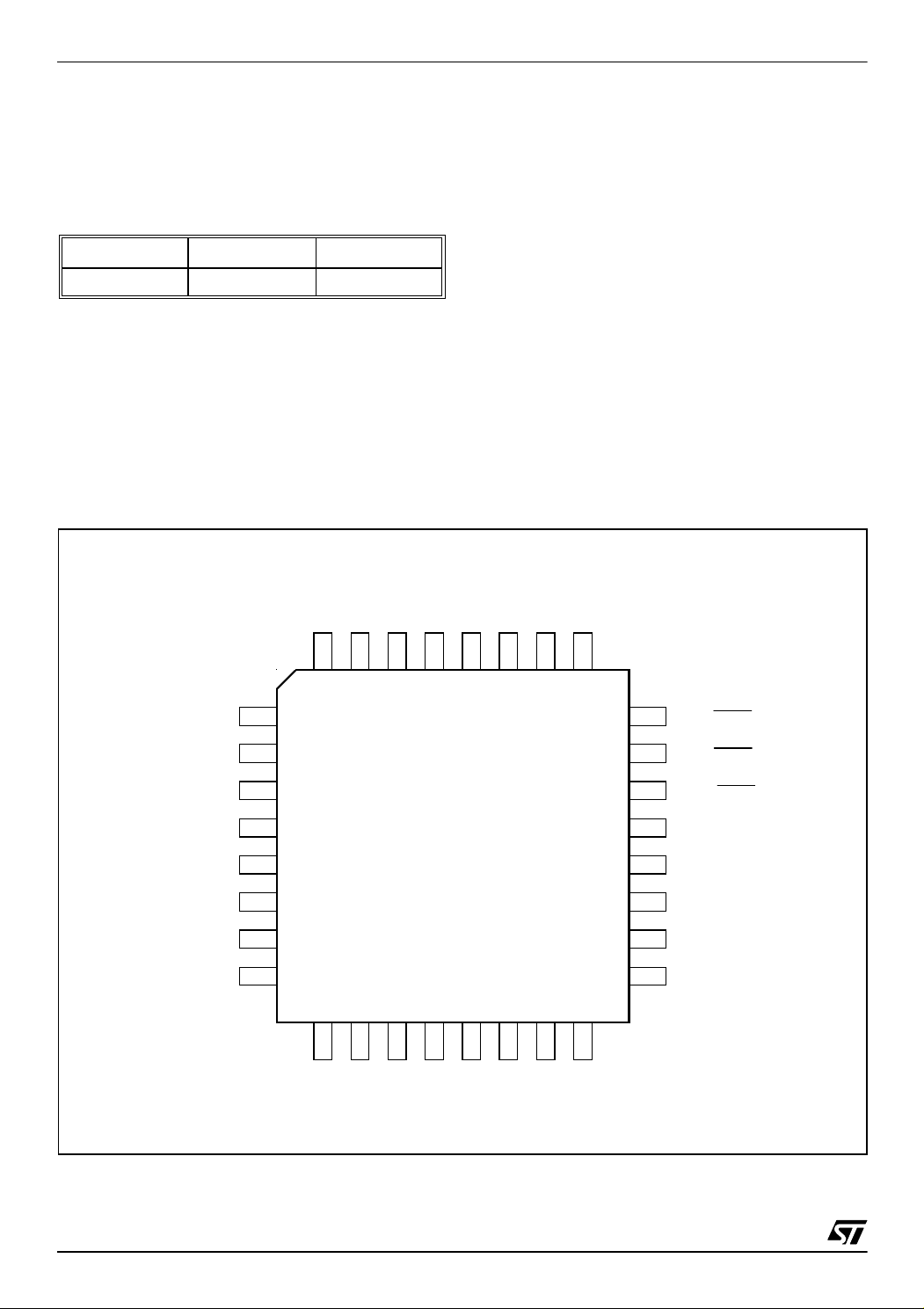
Figure 1.1 TQFP32 Pin Configuration
The CU/DPU can manage up to 334 different
Membership Functions for the fuzzy rules
antecedent part. The rule consequents are “crisp”
values (real numbers). The maximum number of
rules that can be defined is limited by the
dimensions of the implemented standard
algorithm.
EPROM is then shared between fuzzy and
standard algorithms. The Membership Function
data is stored inside the first 1024 memory
locations. The Fuzzy rules are parts of the program
instr uct ion s.
The Cont rol Unit (CU) reads the info rmation an d
the status deriving from the peripherals.
Arithmetic calculus can be performed on these
values by usi ng the internal CU an d the 128/256
bytes of RAM, which supports all computations.
The peripheral input can be fuzzy and/or arithmetic
output, or the val ues contained in Data RAM and
EPROM locations.
INT / PC0
T0OUT / PC1
T1OUT / PC2
T2OUT / PC3
TX / PC4
RX / PC5
PC6
PC7
OSCIN
TEST
32
1
2
3
4
5
6
7
8
9 10 11 12 13
AIN0 / PB0
31
AIN1 / PB1
30 29 28
OSCOUT
AIN2 / PB2
PA0 / T0RES
Vpp
Vss
Vdd
RESET
27 26 25
24
23
22
21
20
19
18
17
14 15 16
Vdda
GNDA
AIN3 / PB3
AIN4 / PB4
AIN5 / PB5
PA1 / T0OUT
PA2 / T1OUT
PA3 / T2OUT
PA4 / STRT
PA5 / T0CLK
PA6
PA7 / PB7 / AIN7
PB6 / AIN6
8/88
Page 9

Figure 1.2 SSO34 Pin Configuration
ST52T430/E430
RESET
OSCOUT
OSCIN
TEST
INT/PC0
T0OUT/PC1
T1OUT/PC2
T2OUT/PC3
TX/PC4
RX/PC5
PC6
PC7
nc
PB0/Ai n0
PB1/Ain1
PB2/A in2
PB3/A in3
Figure 1.3 PSDIP32 Pin Configuration
DD
1
2
3
4
5
6
7
8
9
10
11
12
13
14
15
16
17
34
33
32
31
30
29
28
27
26
25
24
23
22
21
20
19
18
V
Vss
V
PP
PA0/T0RES
PA1/T0OUT
PA2/T1OUT
PA3/T2OUT
PA4/T0STRT
PA5/T0CLK
PA6
PB7/PA 7/Ai n7
PB6/A in6
nc
PB5/Ain5
PB4/Ain4
GNDA
DDA
V
RESET
OSCOUT
OSCIN
TEST
INT/PC0
T0OUT/PC1
T1OUT/PC2
T2OUT/PC3
TX/PC4
RX/PC5
PC6
PC7
PB0/Ain0
PB1/Ain1
PB2/Ain2
PB3/Ain3
1
2
3
4
5
6
7
8
9
10
11
12
13
14
15
16
32
31
30
29
28
27
26
25
24
23
22
21
20
19
18
17
VDD
Vss
PP
V
PA0/T0RES
PA1/T0OUT
PA2/T1OUT
PA3/T2OUT
PA4/T0STRT
PA5/T0CLK
PA6
PB7/PA7/Ain7
PB6/Ain6
PB5/Ain5
PB4/Ain4
GNDA
V
DDA
9/88
Page 10

ST52T430/E430
Table 1.1 ST52x430 SSO34 & PSDIP32 Pin list
SSO34
Pins
SDIP32
Pins
NAME Programming Phase Working Phase
1 1 RESET General Reset General Reset
2 2 OSCOUT Oscillator Output
3 3 OSCIN Oscillator Input
4 4 TEST Must be tied to V
ss Must be tied to Vss
5 5 INT/PC0 PHASE signal (PHASE) External interrupt, Digital I/O
6 6 T0OUT/PC1 Timer/PWM 0 output, Digital I/O
7 7 T1OUT/PC2 Timer/PWM 1 output, Digital I/O
8 8 T2OUT/PC3 Timer/PWM 2 output, Digital I/O
9 9 TX/PC4 SCI Output, Digital I/O
10 10 RX/PC5 SCI Input, Digital I/O
11 11 PC6 Digital I/O
12 12 PC7 Digital I/O
13 nc
14 13 Ain0/PB0 Address Reset (RST_ADD) Analog Input, Digital I/O
15 14 Ain1/PB1 Address Increment (INC_ADD) Analog Input, Digital I/O
16 15 Ain2/PB2 Configuration Reset (RST_CONF) Analog Input, Digital I/O
17 16 Ain3/PB3
Configuration Increment
(INC_CONF)
Analog Input, Digital I/O
18 17 V
DDA Analog Power Supply Analog Power Supply
19 18 GNDA Analog Ground Analog Ground
20 19 Ain4/PB4 Analog Input, Digital I/O
21 20 Ain5/PB5 Analog Input, Digital I/O
22 nc
23 21 Ain6/PB6 Analog Input, Digital I/O
24 22 Ain7/PB7/PA7 I/O EPROM Data Analog Input, Digital I/O
25 23 PA6 I/O EPROM Data Digital I/O
26 24 T0CLK/PA5 I/O EPROM Data Timer/PWM 0 clock, Digital I/O
27 25 T0STRT/PA4 I/O EPROM Data Timer/PWM 0 start/stop, Digital I/O
28 26 T2OUT
/PA3 I/O EPROM Data
29 27 T1OUT/PA2 I/O EPROM Data
30 28 T0OUT/PA1 I/O EPROM Data
Timer/PWM 2 compl. output, Digital I/O
Timer/PWM 1 compl. output, Digital I/O
Timer/PWM 0 compl. output, Digital I/O
31 29 T0RES/PA0 I/O EPROM Data Timer/PWM 0 Reset, Digital I/O
32 30 VPP
33 31 V
34 32 V
DD Digital Power Supply Digital Power Supply
ss Digital Ground Dig ital Ground
EPROM Programming Power
supply (12V ± 5%)
EPROM V
DD or Vss
10/88
Page 11

ST52T430/E430
Table 1.2 ST52x430 TQFP32 Pin list
TQFP32
Pins
1 INT/PC0 PHASE signal (PHASE) External interrupt, Digital I/O
2 T0OUT/PC1 Timer/PWM 0 output, Digital I/O
3 T1OUT/PC2 Timer/PWM 1 output, Digital I/O
4 T2OUT/PC3 Timer/PWM 2 output, Digital I/O
5 TX/PC4 SCI Output, Digital I/O
6 RX/PC5 SCI Input, Digital I/O
7 PC6 Digital I/O
8 PC7 Digital I/O
9 Ain0/PB0 Address Reset (RST_ADD) Analog Input, Digital I/O
10 Ain1/PB1 Address Increment (INC_ADD) Analog Input, Digital I/O
11 Ain2/PB2 Configuration Reset (RST_CONF) Analog Input, Digital I/O
12 Ain3/PB3 Configuration Increment (INC_CONF) Analog Input, Digital I/O
13 V
14 GNDA Analog Ground Analog Ground
15 Ain4/PB4 Analog Input, Digital I/O
16 Ain5/PB5 Analog Input, Digital I/O
21 Ain6/PB6 Analog Input, Digital I/O
22 Ain7/PB7/PA7 I/O EPROM Data Analog Input, Digital I/O
19 PA6 I/O EPROM Data Digital I/O
20 T0CLK/PA5 I/O EPROM Data Timer/PWM 0 clock, Digital I/O
21 T0STRT/PA4 I/O EPROM Data Timer/PWM 0 start/stop, Digital I/O
22 T2OUT
23 T1OUT
24 T0OUT
25 T0RES/PA0 I/O EPROM Data Timer/PWM 0 Reset, Digital I/O
26 V
NAME Programming Phase Working Phase
DDA Analog Powe r Supply Analog Power Supply
/PA3 I/O EPROM Data Timer/PWM 2 compl. output, Digital I/O
/PA2 I/O EPROM Data Timer/PWM 1 compl. output, Digital I/O
/PA1 I/O EPROM Data Timer/PWM 0 compl. output, Digital I/O
PP
EPROM Programming Power supply
(12V ± 5%)
EPROM V
DD or Vss
27 V
28 V
ss Digital Ground Digital Ground
DD Digital Power Supply Digital Power Supply
29 RESET General Reset General Reset
30 OSCOUT Oscillator Output
31 OSC IN Oscillator Input
32 TEST Must be tied to V
ss Must be tied to Vss
11/88
Page 12

ST52T430/E430
1.3 Pin Description V
DD, VSS
, V
, GNDA, VPP. In order to avoid
DDA
noise disturbances, the power supply of the digital
part is kept separate fr om the power supply of the
analog part.
Main Power Supply Voltage (5V± 10%).
V
DD.
. Digital circuit ground.
V
SS
. Analog VDD of the Analog to Digital
V
DDA
Converter.
GNDA. Analog V
Converter. Must be tied to V
of the Analog to Digital
SS
SS
.
VPP. Main P ower Supp ly for interna l EPROM
(12.5V±5%, in programming phase) and MODE
selector. During the Programming phase
(programming), V
Working phase V
must be set at 12V. In the
PP
must be equal to VSS.
PP
OSCin and OSCout. These pins are internally
connected with the on-chip oscillator circuit. A
quartz crystal or a ceramic resonator can be
connected between these two pins in order to allow
the correct operations of ST52x430 with various
stability/cost trade-off. An external clock signal can
be applied to OSCin, in this case OSCout must be
floating.
RESET. This signal is used to restart ST52x430 at
the beginning of its program. It also allows one to
select the program mode for EPROM.
Ain0-Ain8. These 8 lines are conne cted to the
input of the analog multiplexer. They allow t he
acquisition of 8 analog input. During the
Programming phase, Ain0, Ain1, Ain2 and Ain3 are
used to manage EPROM operation.
PA0-PA7, PB0-PB7, PC0-PC7. These lines are
organized as I/O port. Each pin can be configured
as input or output. PA 7/PB7 are t ied to the same
output. During Programming phase PA port is used
for EPROM read/write data.
T0RES, T0CLK, T0STRT. These pins are related
with the in ternal Programm able Timer/P WM 0.
This Timer can be reset externally by using
T0RES. In Working Mode, T0RES resets the
address counter of the Timer. T 0RES is activ e at
low leve l.
The Timer 0 Clock can be the internal clock or can
be supplied externally by using pin T0CLK.
An external Start/Stop signal can be used to
control the Timer through T0STRT pin.
T0OUT, T1OUT, T2OUT. The TIMER/PWM
outputs are available on these pins.
T0OUT
, T1OUT, T2OUT. The TIMER/PWM
complem entary out puts are availa ble on these
pins.
Tx. Serial data output of SCI transm itter block
Rx. Serial data input of the SCI receiver block.
TEST. Duri ng the Programming and Working
phase it must be set to Vss.
12/88
Page 13
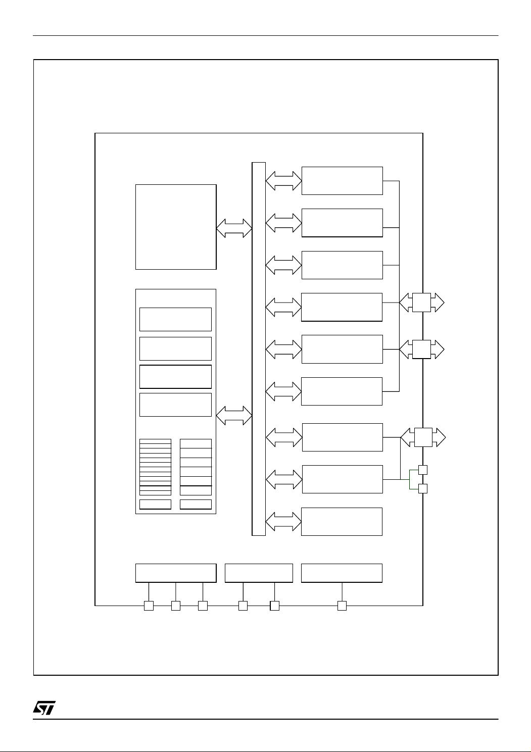
Figure 1.4 ST52X430 Block Diagram
PROGRAM
MEMORY
EPROM
ST52T430/E430
TIMER/P WM 0
TIMER/P WM 1
TIMER/P WM 2
CORE
INTERRUPTS
CONTROLLER
ALU &
DPU
DECISION
PROCESSOR
CONTROL
UNIT
Register File
256 bytes
PC FLAGS
POWER SUPPLY OSCILLATOR
Input
registers
PORT A
PORT C
SCI
PORT B
ADC
WATCHDOG
RESET CIRCUIT
PA7:0
PC7:0
PB7:0
VDDA
GNDA
VDD VPP VSS OSCIN OSCOUT RESET
13/88
Page 14

ST52T430/E430
2 INTERNAL ARCHITECTURE
ST52x430 is made up of the following blocks and
peripherals:
■ Control Unit (CU) and Data Processing Unit
(DPU)
■ ALU / Fuzzy Core
■ EPROM
■ 256 Byte RAM
■ Clock Osc illator
■ Analog Multiplexer and A/D Converter
■ 3 PWM / Timers
■ SCI
■ Digital I/O port
2.1 ST52x430 Operating Modes
ST52x430 works in two modes, Programm ing and
Working Modes, depending on the control signals
level RESET, TEST and V
PP
The Operating modes are selected by setting the
control signal level as specified in the Control
Signals Setting table.
Table 2.1 Control Signals Setting
Control
Signal
RESET V
TEST VSS
VPP 12 V
Pro-
gramming
SS VSS VDD
Reset Workin g
VSS VSS
SS VSS
V
2.2 Control Unit and Data Processing Unit
The Cont rol U nit (CU ) form ally inc ludes five m ain
blocks. Each block decodes a set of instructions,
generating the appropriate control signals. The
main parts of the CU are illustrated in Figure 2.1.
The five different parts of the CU manage Loading,
Logic/Arithmetic, Jump, Control and the Fuzzy
instruction set.
The block called “Co llector” manages the s ignals
deriving from the different parts of the CU, defining
the signals for the Data Processing Unit (DPU) and
the different peripherals of the microcontroller.
The block called “Arbiter” manages the different-
parts of the CU so that only one part of the system
is activated during working mode.
The CU structure is very flexible. It was desig ned
with the purpose of easily adapting the core o f the
microcontroller to market needs. New instruction
sets or new peripherals can be easily included
without changing the structure of the
microcontroller, maintaining code compatibili ty.
The CU reads the instructions stored on EPROM
(Fetch) and decodes them. According to the
instruction types, the arbiter activates one o f the
main blocks of the CU. Afterwards, all the control
signals for the DPU are generated.
A set of 46 different arithmetic, fuzzy and logic
instructions is available. Each instruction requires
6 (fuzzy instructions) to 26 (DIVISION) clock
pulses to be performed.
The DPU receives, stores and sends instructions
deriving from EPROM, RAM or peripherals in order
to execute them.
2.2.1 Program Counter.
The Program Counter (PC) is a 13-bit register that
contains the address of the next memory location
to be processed by the core. This memory location
may be an opcode, operand, or an address of an
operand.
The 13-bit length allows direct addressing of a
maximum of 8,192 bytes in the program space.
After having read the current instruction address,
the PC value is incremented. The result of this
operation is shifted back into the PC.
The PC can be changed in the following ways:
■ JP (Jump)PC = Jump Address
■ InterruptPC = Interrupt Vector
■ RETIPC = Pop (stack)
■ RETPC = Pop (stack)
■ CALLPC = Subroutines address
■ ResetPC = Reset Vector
■ Normal InstructionPC = PC + 1
2.2.2 Flags.
The ST52x430 core includes a different set of
flags that correspond to 2 different m odes : norm al
mode and interrupt mode. Each set of flags consists of a CARRY flag (C), ZERO flag (Z) and
SIGN flag (S).
One set (CN, ZN, SN) is used during normal
operation and one is used during interrupt mode
(CI, ZI, SI). Formally, t he user has to manage
only one set of flags: C, Z and S.
14/88
Page 15

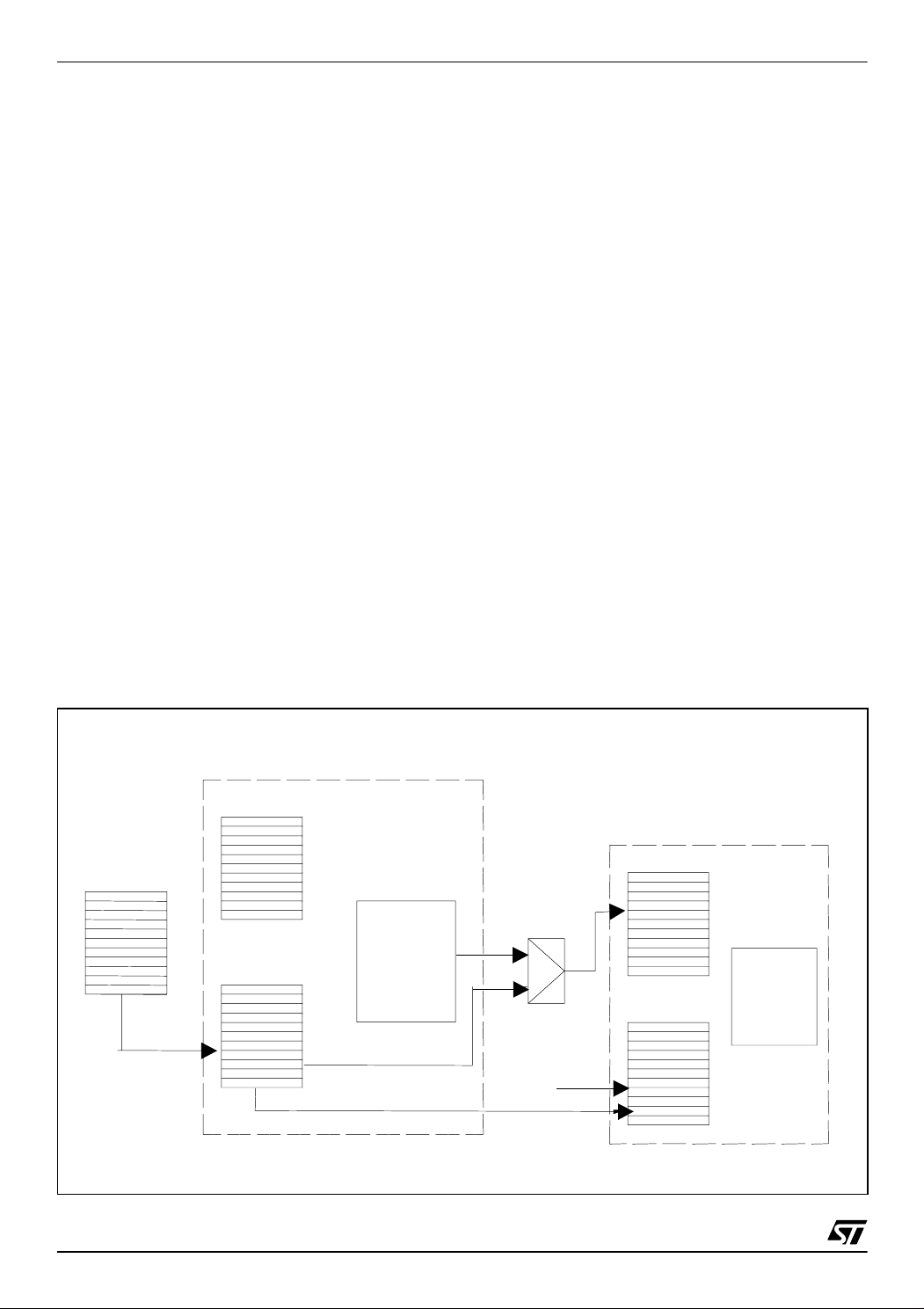
Figure 2.1 Data Processing Unit (DPU)
ST52T430/E430
CU
EPROM
INPUTS
PERIPHERALS
ADDRESS RAM
STACK POINT
M
U
X
Figure 2.2 CU/DPU Block Diagram
PROGRAM CO U NTER
RAM
256 Bytes
ACCUMU LATOR
FLAGS REG.
PERIPHERALS
FUZZY
REGISTERS
MULTIPLEXER
ALU
add_EPR
E
P
R
O
M
M icrocode
RAM
C
U
Control S ignals
EP RO M A ddress
RAM Data 8 Bit
RAM A ddr.
8 Bit
RAM
D a ta O u t
8 Bit
D
P
U
To Peripherals
From
Pe riph erals
15/88
Page 16
ST52T430/E430
The ST52x430 core us es flags that correspond to
the actual mode. As soon as an interrupt is
generated the ST52x430 core uses the interrupt
flags instead of the normal flags.
Each interrupt level has its own set of flags, which
is saved in the STAC K toge ther with the Program
Counter. These flags are restored from the STACK
automatically when a RETI instruction is executed.
If the MCU was in normal mode before an interrupt,
the normal flags are restored when the RETI
instruction is executed.
Note:
A CALL subroutine is a normal mode
execution. For this reason, a RET instruction,
consequent to a CALL ins truction does not affect
the normal mode set of flags.
Flags are not cleared during context switching and
remain in the state they were at the end of the last
interrupt routine switching.
The Carry flag is set when an overflow occurs
during arithmetic operations, otherwise it is
cleared.
The Sign flag is set when an underflow occurs
during arithmetic operations, otherwise it is
cleared.
2.3 Address Spaces
ST52x430 has four separate address spaces:
■ RAM: 256 Bytes
■ Input Registers: 20 8-bit registers
■ Output Registers 10 8-bit registers
■ Configuration Registers: 21 8-bit registers
■ Program memory up to 8K Bytes
Program memory will be described in further
details in the MEMORY sec t io n
2.3.1 RAM and STACK.
RAM memory consists of 256 general purpose 8bit RAM registers.
All the registers in RAM can be specified by using
a decimal address. For e xample, 0 identifies the
first register of RAM.
To read or write RAM registers LOAD instructions
must be used. See Table 2.5
Each interrupt level has its own set of flags, which
is saved in the STAC K together w ith the P rogram
Counter. These flags are restored from the STACK
automatically when a RETI instruction is executed.
When the instructions like Interrupt request or
CALL are executed, a STACK level is used to push
the PC.
The STACK is located in RAM. For each l evel of
stack, 2 bytes of RAM are used. The values of this
stack are stored from the last RAM register
(address 255). The maximum level of stack
must be less than 128.
Figure 2.3 Address Spaces Description
ST52X430 CORE
PROGRAM MEMORY
INPUT REGISTERS
CONTROL UNI T
RAM
LDRI
DPU
ALU
LDRC
LDCR
LDPR
LDCE
ON CHIP PERIPHERALS
PERIPHERAL REGISTERS
CONFIGURATION
REGISTERS
PERIPHERAL
BLOCK
16/88
Page 17

ST52T430/E430
The STACK POINTER indicates the first level
available to store data. When a subrou tine call or
interrupt request occurs, the content of t he PC and
the current set of flags are stored into the level
located by the STACK POINTER.
When a interrupt return occurs (RETI instruction),
the data stored in the highest stack level is
restored back into the PC and current flags.
Instead, when a subroutine return occurs (RET
instruction) the data stored in the highest stack
level are restored in the PC not affecting the flags.
These operating modes are illustrated in Figure
2.4.
The user must pay close attention to avoid
Note:
overwriting RAM locations where the STACK could
be stored
.
2.3.2 Input Registers Bench.
The Input Registers (IR) bench consists of 20 8-bit
registers containing data or the status of the
peripherals.
Figure 2.4 Stack Operation
All the registers can be specified by using a
decimal address (for exam ple, 0 identifies the first
register of the IR).
The assembler instruction:
LDRI RAM_Reg. IR_i
loads the value of the i-th IR in the RAM location
identified by the RAM_Reg address.
The first input register is dedicated to store the
value of the stack pointer. The next 8 registers
(ADC_OUT_0:7) of the IR are dedicated to t he 8
converted values deriving from the ADC. The last
9 Input Registers contain data from the I/O ports
and PWM/Timers. The following table summarizes
the IR address and the relative peripherals. In
order to simplify the concept, a mnemonic name is
assigned to the registers. The same name is used
in VISUALSTUDI O
®
development tools
REG 0
REG 1
REG 2
REG 3
REG 4
REG 5
WHEN RETI OR RET
OCCURS
REG 252
REG 253
REG 254
REG 255
PRO G RAM CO U NTER
RAM
WHEN CALL OR
INTERRUPT REQ.
OCCURS
Stack
Pointer
STACK LEVEL n
..........................
STACK LEVEL 2
STACK LEVEL 1
17/88
Page 18

ST52T430/E430
Table 2.2 Input Registers
IR MNEMONIC NAME PERIPHERAL REGISTER ADDRESS
STACK_POINTER STACK POINTER 0
CHAN 0 A/D CHANNEL 0 1
CHAN 1 A/D CHANNEL 1 2
CHAN 2 A/D CHANNEL 2 3
CHAN 3 A/D CHANNEL 3 4
CHAN 4 A/D CHANNEL 4 5
CHAN 5 A/D CHANNEL 5 6
CHAN 6 A/D CHANNEL 6 7
CHAN 7 A/D CHANNEL 7 8
PORT_A PORT A INPUT REGISTER 9
PORT_B PORT B INPUT REGISTER 10
PORT_C PORT C INPUT REGISTER 11
PWM_ 0_COUNT PWM/TIMER 0 COUNTER 12
PWM_ 0_ STATUS PWM/TIMER 0 STATUS REGISTER 13
PWM_ 1_ COUNT PWM/TIMER 1 COUNTER 14
PWM_ 1_ STATUS PWM/TIMER 1 STATUS REGISTER 15
PWM_ 2_ COUNT PWM/TIMER 2 COUNTER 16
PWM_ 2_ STATUS PWM/TIMER 2 STATUS REGISTER 17
SCI_RX SCI DATA REGISTER 18
SCI_STATUS SCI STATUS REGISTER 19
2.3.3 Configuration Registers.
The ST52x430 configuration Registers allow the
configuration of all the blocks of the fuzzy
microcontroller. Table 2.3 describes the functions
and the related peripherals of each of the
instructions, the Configuration Registers can be
set by using values stored in the Program Memory
(EPROM) or in RAM.
Use and meaning of each register will be described
in further details in the corresponding section.
Configuration Registers. By using the load
Table 2.3 Configuration Registers
CONFIGURATION REGISTER PERIPHERAL DESCRIPTION
REG_CONF 0 INTERRUPT MASK Interrupts mask setting
REG_CONF 1 N.U. N.U.
REG_CONF 2 WATCHDOG TIMER Watchdog Timer Configuration
REG_CONF 3 A/D CONVERTER A/D configuration
18/88
Page 19

Table 2.3 Configuration Registers (continued)
CONFIGURATION REGISTER PERIPHERAL DESCRIPTION
ST52T430/E430
REG_CONF 4 PORT A
REG_CONF 5 PWM/TIMER 0
REG_CONF 6 PWM/TIMER 0
REG_CONF 7 PWM/TIMER 0
REG_CONF 8 PWM/TIMER 1
REG_CONF 9 PWM/TIMER 1
REG_CONF 10 PWM/TIMER 2
REG_CONF 11 PWM/TIMER 2
REG_CONF 12 PORT A
REG_CONF 13 PORT B
Set the relative bit like digital input
or digital output
PWM/Timer 0 Working mode
Configuration
PWM/TIMER 0 Prescaler
configuration and output waveform
selection.
PWM/TIMER 0 Working Mode
Configuration
PWM/TIMER 1 Working Mode
Configuration
PWM/TIMER 1 Prescaler
configuration and output waveform
selection.
PWM/TIMER 2 Working Mode
Configuration
PWM/Timer 2 Prescaler
configuration and output waveform
selection.
Set the bit 0,1 and 2 like Digital I/O
or complementary Timers Output.
Set the relative bit like digital input
or digital output.
REG_CONF 14 PORT B
REG_CONF 15 PORT C
REG_CONF 16 PORT C
REG_CONF 17 Interrupt Priority Set the Interrupts priority
REG_CONF 18 Interrupt Priority Set the Interrupts priority
REG_CONF 19 SCI Set the SCI working mode
REG_CONF 20 SCI Set the SCI working mode
2.3.4 Output Registers.
The Output Registers (OR) consist of 10 registers
containing data for the microcont roller peripherals
including the I/O Ports.
All registers can be specified by us ing a decimal
address (for example, 1 identifies the second OR).
By using LOAD instructions t he Output Registers
(OR) may be set by using values stored in the
Program Memory (LDPE) or in RAM (LDPR)
The assembler instruction:
LDPR OR_i RAM_Reg.
Set the relative I/O like Digital or
Analog.
Set the relative I/O like digital input
or digital output
Set the relative I/O like Digital I/O
or Timers Output
loads the value of the RAM location identified by
the address RAM_Reg in the OR i-th Table 2.4
describes OR.
In order to simplify the concept, a mnemonic name
is assigned to OR. T he same names are used in
FUZZYSTUDIO
TM
4.0 development tools.
Use and meaning of each register will be described
in further details in the corresponding section.
19/88
Page 20
ST52T430/E430
Table 2.4 Output Registers
OR MNEMONIC NAME PERIPHERAL REGISTER ADDRESS
PORT_ A PORT A OR 0
PORT_ B PORT B OR 1
PORT_C PORT C OR 2
PWM_0_COUNT TIMER/PWM 0 COUNTER 3
PWM_0_RELOAD TIMER/PWM 0 RELOAD REGISTER 4
PWM_1_COUNT TIMER/PWM 1 COUNTER 5
PWM_1_RELOAD TIMER/PWM 1 RELOAD REGISTER 6
PWM_ 2_ COUNT TIMER/PWM 2 COUNTER 7
PWM_2_RELOAD TIMER/PWM 2 RELOAD REGISTER 8
SCI_TX_DATA SCI DATA REGISTER 9
2.4 Arithmetic Logic Unit
The 8-bit Arithmetic Logic Unit (ALU) allows the
performance of arithmetic calculations and logic
instructions, which can be divided into 5 groups:
Load, Arithmetic, Jump, Interrupts and Program
Control instructions (refer to the ST52x430
Assembler Set for further details).
The computational time required for each
The ALU of the ST52x430 can perform
multiplication (MULT) and division (DIV).
Multiplication is performed by using 8 bit operands
storing the result in 2 registers (16 bit values), see
Figure 2.5 and Figure 2.6.
WARNING: If the LSB of the multiplication
result is 0, the Zero flag is set although the
result is not 0.
instruction consists of one clock pulse for each
Cycle plus 3 clock pulses for the decoding phase.
Table 2.5 Load instructions
Load Instructions
Mnemonic Instruction Bytes Cycles Z S C
LDCE LDCE conf, EPROM 3 17 - - -
LDCR LDCR conf, RAM 3 14 - - -
LDFR LDFR FUZZY_i_RAM RAM 3 14 - - LDPE L DPE per, EPROM 3 17 - - LDPE LDPE per, (RAM) 3 17 - - LDPR LDPR reg, RAM 3 14 - - -
LDRC LDRC RAM, const 3 14 - - -
LDRE LDRE RAMi, EPROMi 3 16 - - LDRE LDRE (RAMi), (RAMj) 3 18 - - -
LDRI LDRI RAM, inp_reg 3 15 - - -
LDRR LDRR RAMi, RAMj 3 16 - - -
20/88
Page 21

ST52T430/E430
Table 2.5 Load instructions
PGSET PGSET const 2 9 - - -
Table 2.6 Arithmetic & Logic instructions set
Arithmetic Instructions
Mnemonic Instruction Bytes Cycles Z S C
ADD ADD regi, regj 3 17 I - I
ADDO ADDO regi, regj 3 20 I I I
AND AND regi, regj 3 17 I - -
ASL ASL regi 2 15 I - I
ASR ASR regi 2 15 I I DEC DEC regi 2 15 I I -
DIV DIV regi, regj 3 26 I I I
INC INC regi 2 15 I - I
MULT MULT regi, regj 3 19 I - -
NOT NOT regi 2 15 I - -
OR OR regi, regj 3 17 I - -
SUB SUB regi, regj 3 17 I I -
SUBO SUBO regi, regj 3 20 I I I
MIRROR MIRROR regi 2 15 I - -
Table 2.7 Jump Instruction Set
Jump instructions
mnemonic instruction bytes cycles z s c
call call addr 3 18 - - -
jp jp addr 3 12 - - -
jpc jpc addr 3 10/12 - - jpnc jpnc addr 3 10/12 - - jpns jpns addr 3 10/12 - - jpnz jpnz addr 3 10/12 - - -
jps jps addr 3 10/12 - - -
jpz jpz addr 3 10/12 - - -
ret ret 1 13 - - -
Table 2.8 Interrupt Instructions Set
Interrupt Instructions
Mnemonic Instruction Bytes Cycles Z S C
HALT HALT 1 7/15 - - -
MEGI MEGI 1 7/15 - - -
21/88
Page 22
ST52T430/E430
Table 2.8 Interrupt Instructions Set (continued)
MDGI MDGI 1 6 - - -
RETI RET I 1 12 - - -
RINT RINT INT 2 8 - - -
UDGI UDGI 1 6 - - -
UEGI UEGI 1 7 /15 - - -
WAITI WAITI 1 7 /14 - - -
Table 2.9 Control Instructions Set
Control Instructions
Mnemonic Instruction Bytes Cycles Z S C
FUZZY FUZZY 1 5 - - -
NOP NOP 1 6 - - -
WDTRFR WDTRFR 1 7 - - -
WDTSLP WDTSLP 1 6 - - -
Notes:
I affec ted
- not affected
Figure 2.5 Multiplication Figure 2.6 Division
RAM
0
1
2
i-1
i
i+1
j-1
j
j+1
253
254
255
REG. j REG. j+1
REMAINDER QUOTIENT
:
REG. i
REG. j REG. i
LSB
RAM
0
1
2
i
j-1
j
j+1
253
254
255
X
16 Bit
MSB
22/88
Page 23
ST52T430/E430
3 EPROM
EPROM memory provides an on-chip userprogrammable non-volatile m emory, which allows
fast and reliable storage of user data.
EPROM memory can be locked by the user. In
fact, a memory location called Lock Cell is devoted
to lock EPROM and avoid external ope rations. A
software identification code, called ID CODE,
distinguishes which softw are version is stored in
the memo r y .
64 kbits of memory space with an 8-bit internal
parallelism (up to 8 kbytes) addressed by an 13-bit
bus are available. The data bus is 8 bits.
Memory has a double supply: V
12V±5% in Programming Phase or to V
Working Phase. V
is equal to 5V±10%.
DD
is equal to
PP
during
SS
ST52x430 EPROM memory is divided into three
main blocks (see Figure ):
■
Interrupt Vectors memory block
(3 through 20)
contains the addresses for the interrupt routines.
Each address is composed of three bytes.
■
Mbfs Setting memory block
MemAdd
) contains the coordinates of the
(21 through
vertexes of every Mbf defined in the program.
■ The maximum value of MemAdd is 1023. This
area is dynamically assigned according to the
size of the fuzzy routines. The unused memory
area, if any, is assigned to the Program
Instruction Set memory block.
■ The Program Instructions Set memory block
(MemAdd through MemAddx) contains the
instruction set of the user program. The
following table summarizes the values of Mem
Addx for the different devices
Table 3.1 Mem Addx
ST52T430K1 ST52T430 ST52T430
Me
m
2047 4095 8191
Locations 0, 1 and 2 contain the address of the first
microcode instruction.Th e operations that can be
performed on EPROM during the Programming
Phase are: Stand By, Memory Writing, Reading
and Verify/Margin Mode, Memory Lock, IDCode
Writing and Verify.
Figure 3.1 Pro gra m M em ory Organizati on
ST52430K3
ST52430K2
ST52430K1
MemAdd+1
MemAdd
8191
4095
2047
21
20
Fuzzy and Boolean
Algorithms
Mbfs Parameters
INT_EXT
INT_SCI
INT_TIMER/PWM2
INT_TIMER/PWM1
INT_TIMER/PWM0
3
2
0
INT_ADC
Program Instruction
First Address
Program
Instruction
Set
Mbfs Setting
and Program
Instruction Set
Interrupt
Vectors
23/88
Page 24
ST52T430/E430
MEMORYVER
MARGINMOD
D
OUTV
D
VALIDDATA
DATAOUT
Table 3.2 EPROM Control Register
OPERATION REGISTER VALUE
Stand By 0
Memory Reading/Verify 1
The operations ab ove are managed by us ing the
internal 4-bit EPROM Control Register. The
reading phase is executed with V
the verify/Margin Mode phase needs V
5V±5%, while
PP=
PP
12V±5%. The Blank Check must be a reading
operation with V
PP=
5V±5%.
Table 3.2 illustrates EPROM Control Register
codes used to identify the operation running.
=
Memory Unlock and
Lock Status Reading
2
Memory Writing 3
Memory Lock 4
ID CODE Writing 5
Memory Lock Status
Reading/Verify
ID CODE Reading/
Verify
9
10
Figure 3.2 Eprom Programmi ng Timing
PA(0:7)
RST_ADD
ALID
ATA
ATA
3.1 EPROM Programming Phase Procedure
The Programming mode is selected by applying
12V±5% voltage or 5V ±5% voltage to the V
PP
pin
and setting the control signal as following:
RESET =Vss
TEST =Vss
If the V
performed.
voltage is 5V±5% only readi ng may be
PP
RST_ADD, INC_ADD, RST_CONF, INC_CONF
and PHASE are the control signals used during the
Programming Mode.
PHASE, RST_CONF and RST_ADD signals are
active on level, the others are active on rising
edge.
VALID
DATA
DATA
IN
DATA
OUT
RST_CONF
INC_ADD
INC_CONF
PHASE
MEMORY UNLOCK
24/88
100nS
MEMORY WRITING
LOCATION ADDRESS =1
10
S
µ
IFY
E
Page 25

ST52T430/E430
PHASE and RST_ADD signals are active low,
RST_CONF signal is active high.
Port A is used for the memory data I/O.
(See Table
3.2 for pin reference on the different packages)
Memory may be locked by means of the Memory
Lock Status, which is a flag used to enable
EPROM operations.
If Memory Lock Status is 1 all EPROM operations
are enabled, otherwise the user may only read
(and verify) the OTP code and the Memory Lock
Status.
Only if EPROM is not locked by means of Lock Cell
(see EPROM Locking may E PR O M o perations be
enabled by changing the Memory Lock Status from
0 to 1.
RST_ADD signal resets the memory address
register and the Memory Lock Status. When the
RST_ADD becomes high, the memory must be
unlocked in order to read or write.
INC_ADD signal increments the memory address.
RST_CONF signal resets the EPROM Control
Register. When RST_CONF is high, the DATA I/
O Port A is in outpu t, ot her wise it is alwa ys in
inpu t.
INC_CONF signal increments the EPROM Control
Register value.
PHASE signal validates the operation selected by
means of the EPROM Control Register value.
3.1.1 EPROM Operati on.
In order to execute an EPROM operation (See
Table 3.2), the corresponding identification value
must be loaded in the EPROM Control Register.
The signal timing is the f ollowing: RST_ADD= high
and PHASE= high, RST_CONF changes from low
to high level, to reset the EPROM Control Register,
and INC_CONF signal generates a number of
positive pulses equal to the value to be loaded.
After this sequence, a negative pulse of the
PHASE signal will validate the operation selected.
The minimum PHASE signal pulse width must be
10 µs for EPROM Writing Operation and 100 ns for
the others.
When RST_CONF is high, DATA I/O Port A is
enabled in output and the reading/verifying
operation results are available.
After a writing operation, when RST_CONF is high,
Port A is in output without valid data.
3.1.2 EPROM Locking.
The Memory Lock operation, which is identified
with the number 4 in the EPROM Control Register,
.
writes “0 " in t he Memory Loc k Cell.
At the beginning of an External Operation, when
the RST_ADD signal changes from low level to
high level, the Memory Lock Status is “0", therefore
it must be unlocked before proceeding.
In order to unlock the Memory Lock Status the
operation, which is identified by the number 2 in
the EPROM Control Register must be executed
(see Figure 3.2).
Memory Lock Status can be changed only if
Memory Lock Cell is “1". After a Memory Lock
operation external operat ions cannot b e executed
except to read (or veri fy) the OTP Code and the
Memory Lock Status.
3.1.3 EPROM Writing.
When the memory is blank, all bits are at logic level
“1". Data is introduced by programming only the
zeros in the desired memory location. However, all
input data must contain both ”1" and “0".
The only way to change “0" into ”1" is to erase the
entire memory (by exposure to Ultra Violet light)
and reprogram it.
The memory is in Writing mode when the EPROM
Control Register value is 3.
The V
voltage must be 12V±5%, with stable data
PP
on the data bus PA(0:7).
The timing signals are the following (see Figure ):
1) RST_ADD and RST_CONF change from low to
high level,
2) two pulses on INC_CONF signal load the
Memory Unlock operation code,
3) a negative pulse (10 0 ns) on the PHASE signal
validates the Memory Unlock operation,
4) a negative pulse on RST _CONF signal resets
the EPROM Control Register,
5) three positive pulses on INC_CONF load the
Memory Writing operation code,
6) a train of positive pulses on INC_ADD signal
increments the memory location address up to the
requested value (generally this is a sequential
operation and only one pulse is used),
7) a negative pulse (10 µs) on the PHASE signal
validates the Memory Writing operation.
25/88
Page 26

ST52T430/E430
3.1.4 EPROM Read/Verify Margin Mode.
The read phase is executed with V
instead of the verify phase that needs V
PP=
5V±5%,
PP
12V±5%.
The Memory Verify operation is available in order
to verify the accuracy of the data written. A
Memory Verify Margin Mode operation can be
executed immediately after writing each byte, in
this case (see Figure ):
1) a positive pulse on RST_CONF signal resets the
EPROM Control Register, if it wasn’ t already reset;
2) one positive pulse on INC_CONF loads the
Memory Read/Verify operation code;
3) a negative pulse (100 n s) o n t he PH AS E signal
validates the Memory Reading / Verify operation;
4) a negative pulse on RST_CONF signal put s in
the PA(0:7) port the value stored in the actual
memory address and resets the EP ROM Control
Register;
If an error occurred writing, the user has to repeat
EPROM writing.
3.1.5 Stan d by M ode.
EPROM has a standby m ode, which reduces the
active current from 10mA (Programming mode) to
less than 100 µA. Memory is placed in standby
mode by setting the PHASE signal at a high level
or when the EPROM Control Register value is 0
and the PHASE signal is low.
3.1.6 ID code.
A software identification code , cal led ID c ode m ay
=
be written in order to distinguish which software
version is stored in the memory.
64 Bytes are dedicated to store this code by using
the address values from 0 to 63.
The ID Code may b e read or verified even if the
Memory Lock Status is “0".
The timing signals are the same as that of a normal
operation.
3.2 Eprom Erasure
The transparent window available in the
CSDIP32W package, allows the memory co ntents
to be erased by exposure to UV light.
Erasure begins when the device is exposed to light
with a wavelength shorter than 4000Å. Sunlight, as
well as some types of artificial light, includes
wavelengths in the 3000-4000Å range which, on
prolonged exposure can cause erasure of memory
contents. Therefore, it is recommended that
EPROM devices be fitted with an opaque label
over the window area in order to prevent
unintentional erasure.
The erasure procedure recommended for EPROM
devices consists of exposure to short wave UV
light having a wavelength of 2537Å. The m inimum
integrated dose recommended (intensity x exposure time) for complete erasure is 15Wsec/cm 2.
This is equivalent to an erasure time of 15-20
minutes using a UV source having an in tensity of
12mW/cm 2 at a distance of 25mm (1 inch) from
the device window.
26/88
Page 27

ST52T430/E430
Global Interrupt
4 INTERRUPTS
The Control Unit (CU) responds to peripheral
events and external events via its interrupt
channels.
When such an events occur, if the related interrupt
is not masked and according to a priority order, the
current program execution can be suspended to
allow the CU to execute a specific response
routine.
Each interrupt is associated with an interrupt
vector that contains the memory address of the
related interrupt service routine. Each vector is
located in the Program Space (EPRO M Memory)
at a fixed address (see Interrupt Vectors Table
4.2).
4.1 Interrupt Operation
If there are pending interrupts at the end of an
arithmetic or logic instruction, the one with the
highest priority is passed. Passing an interrupt
means storing the arithmetic flags and the current
PC in the stack and executing the associated
Interrupt routine, whose address is located in three
bytes of the EPROM memory location between
address 3 and 20.
The Interrupt routine is performed as a normal
code, checking if a higher priority inte rrupt has to
be passed at the end of each instruction. An
Interrupt request with the higher priority stops the
lower priority Interrupt. The Program Counter and
the arithmetic flags are stored in the stack.
With the RETI (Return from Interrupt) instruction
the arithmetic flags and Program Counter (PC) are
restored from the top of the stack. This stack wa s
already described in section RAM and STACK.
An Interrupt request cannot stop processing of the
fuzzy rule, but this is passed only after the end of
a fuzzy rule or at the end of a logic, or arithmetic
instruction.
NOTE: A fuzzy routine can only be interrupted
in the Main program. An interrupt request
cannot stop a Fuzzy function that is running
inside another interrupt routine. In order to use
a Fuzzy function inside an interrupt routine, the
user MUST include the Fuzzy function between
an UDGI (MDGI) instruction and an UEGI
(MEGI) instruction (see the following
paragraphs), so that the interrupt request m ay
be disabled during the executio n of the fuzzy
function.
Figure 4.1 Interrupt Flow
NORMAL
PROGRAM
FLOW
INTERRUPT
SERV ICE
ROUTINE
INTERRUP T
RETI
INSTRUCTION
Figure 4.2 Interrupt Vectors mapping
3
4
INT_ADC
5
6
7
INT_TIMER/PWM0
8
9
10
INT_TIMER/PWM1
11
12
13
INT_TIMER/PWM2
14
15
16
INT_SCI
17
18
INT_EXT
19
20
INTERRUPT
VECTORS
Figure 4.3 Global Interrupt Request generation
Global In te rr up t
Pending
Reque st
User Global
Interr up t Mas k
4.2 Global Interrupt Request Enabling
When an Interrupt occurs, it generates a Global
Interrupt Pending (GIP), that can be masked by
software. After a GI P a Global Interrupt Reques t
(GIR) will be generated and Interrupt service
Macro Global
27/88
Page 28

ST52T430/E430
Routine associated to the interrupt with higher
priority will start.
In order to avoid possible conflicts between
interrupt masking set in the main program, or
inside high level language compiler macros, the
GIP is hung up through the User Global I nterrupt
Mask or the Macro Global Interrupt Mask (see
Figure 4.2).
UEGI/UDGI instruction switches on/off the User
Global Interrupt Mask, enabl ing/disabling the GIR
for the main program.
MEGI/MDGI instructions switch t he Macro Global
Interrupt Mask on/off, in order to ensure that the
macro will not be broken.
4.3 Interrupt Sources
ST52x430 manages interrupt signals generated by
the internal peripherals (PWM/Timers, UART and
Analog to Digital Converter) or coming from the
INT/PC0 pin. The External Interrupt can be
programmed to be active on the rising or falling
edge of INT/PC0 signal by setting the PEXTIN T bit
of the Configuration Register to 0.
WARNING:
interrupt request is generated.
Each peripheral can be programmed in order to
generate the associated interrupt; further details
are described in the related chapter.
4.4 Interrupt Maskability
The interrupts can be masked by configuring the
REG_CONF 0 by means of LDCR, or LDCE,
instruction. The interrupt is enabled when the bit
associated to the mask interrupt is “1". Viceversa,
when the bit is ”0", the interrupt is ma sked and is
kept pendent.
For example:
LDRC 10,6 //load the constant 6 in the
RAM Register 10
LDCR 0, 10 // set the CONF_REG 0 with
the value stored in the RAM Register
10
the result is CONF_REG0 =00000110 enabling the
interrupts deriving from the ADC (INT_ADC) and
from the PWM/TIMER 0 (INT_PWM/TIMER0).
Changing the interrupt priority an
Table 4.1 Configuration Register 0
Description
Bit Name Value Description
0
0MSKE
1
0
1 MSKAD
1
0
2 MSKTM0
1
0
3 MSKTM1
1
0
4 MSKTM2
1
0
5MSCI
1
0
6 PEXTINT
1
External Interrupt
Masked
External Interrupt
Not Masked
A/D Converter
Interrupt
Masked
A/D Converter
Interrupt
Not Masked
PWM/TIMER
0Interrupt
Masked
PWM/TIMER 0
Interrupt
Not Masked
PWM/TIMER 1
Interrupt
Masked
PWM/TIMER 1
Interrupt
Not Masked
PWM/TIMER 2
Interrupt
Masked
PWM/TIMER 2
Interrupt
Not Masked
SCI Interrupt
Masked
SCI Interrupt Not
Masked
External Interrupt
Polarity
Active on Rising
External Interrupt
Polarity
Active on Falling
28/88
7 Not used
Reset Configuration ‘000000’
Page 29

Table 4.2 Interrupts Description
ST52T430/E430
Name Description Priority
INT_ADC ADC Int Programmable 000 yes 3-5
INT_PWM/
TIMER0
INT_PWM/
TIMER1
INT_PWM/
TIMER2
INT_SCI SCI Int Programmable 100 yes 15-17
INT_EXT
Figure 4.4 Interrupt Configuration Register 0
PWM/TIMER 0 Int Programmable 001 yes 6-8
PWM/TIMER 1 Int Programmable 010 yes 9-11
PWM/TIMER 2 Int Programmable 011 yes 12-14
External
Interrupt (INT)
Ext Highest - yes 18-20
Peripheral
Code
Maskable
REG_CONF0
Interrupts Mask
EPROM
Locations
D0
D1D2D3D4D5D6D7
MSKE: Ext. Int.
MSKAD: A/D Int.
M SK TM0 : Time r 0 I n t.
M SK TM1 : Time r 1 I n t.
M SK TM2 : Time r 2 I n t.
M SCI: SC I In t.
PEXTINT: Ext. Int. Polariry
Not Used
29/88
Page 30

ST52T430/E430
Figure 4.5 Interrupt Configuration Register 17 & 18
Interrup ts P rior ity
REG_CONF1 8
D10D1 1D12D13D14D15
D8D9
4.5 Interrupt Priority
Seven priority levels are available: level 6 has the
lowest priority, level 0 has the highest priority.
Level 6 is associated to the Main Program, levels 5
to 1 are programmable by means of the priority
registers called REG_CONF17 and
REG_CONF18 (see Figure 4.5 and Table 4.3);
whereas the higher level is related to the external
interrupt (INT_EXT).
PWM/Timers, UART and ADC are ident ified by a
three-bit Peripheral Codes (see Table 4.2); in order
i
to set the
peripheral label
-th priority level the user must write the
i
in the related INTi priority le v el.
i.e.
LDRC 10, 193 //(load the value
193=’11000001’ in the RAM Register 10)
LDRC 11, 168 //(load the value
168=’10101000’ in the RAM Register 11)
LDCR 17, 10 // set the REG_CONF17=
‘11000001’
LDCR 18, 11 // set the REG_CONF18=
‘10101000’
The following priority levels are defined:
■ Level 1: INT_PWM/TIMER0 (PWM/TI MER 0
Code: 001)
■ Level 2: INT_ADC (ADC Code: 000)
REG_CONF17
D0D1D2D3D4D5D6D7
INT 1
INT 2
INT 3
INT 4
INT 5
Not Used
Table 4.3 Conf. Register 17 & 18 Description
Bit Name Value Level
0, 1,2 INT1
3, 4,5 INT2
6,7,8 INT3
9,10,11 INT4
12,13,1
4
■ Level 3: Int_PWM/Timer2 (PWM/TIMER 2
INT5
Periphera
l Code
Periphera
l Code
Periphera
l Code
Periphera
l Code
Periphera
l Code
High
Medium-High
Medium-Low
Low
Very Low
Code: 011)
■ Level 4: INT_UART (UART Code: 100)
■ Level 5: INT_PWM/TIMER1 (PWM/TIMER 1
Code: 010)
30/88
Page 31

Figure 4.6 Examp le of a sequence of Interrupt req uests
Table 4.4 RINT Instruction code
PRIORITY
LEVEL
0
INT2 INT0 INT4 INT1 INT3
INT0
ST52T430/E430
Peripheral Name Value
PWM/TIMER 1 2
1
2
3
4
5
6
MAIN PROGRAM
INT2
REMARK: The Interrupt priority must be set at
the beginning of the main program, because at
the RESET REG_CONF1=’00000000’, this
condition could generate wrong operations.
Further, changing the priority levels must be
avoided in interrupt service routines.
When a source provides an In terrupt request and
the request processing is also enabled, the CU
changes the normal sequential flow of a program
by transferring program control to a selected
service routine.
When an interrupt occurs the CU executes a JUMP
instruction to the address loaded in the related
location of the Interrupt Vector.
When the execution returns to the original program
it immediately begins following the in struction that
was interrupted.
INT1
INT2
PWM/TIMER 2 3
SCI 4
INT2
External Interrupt 5
INT3
INT4
MAIN PROGRAM
4.6 Interrupts and Low power mode
All interrupts allow the processor to leave the WAIT
low power mode. Only the external Interrupt allows
the processor to leave the HALT low power mode.
4.7 Interrupt RESET
An eventually pending interrupt can be reset with
the instruction RINT j, which rese ts the interrupt
j
-th where j identifies the peripherals as described
in the following table (see Table 4.4).
The assembler instruction:
RINT 2
Resets the PWM/Timer 1 interrupt.
Note: The RINT command must be preceded
from a UDGI (or M DGI ) co mm and an d followed
by a UEGI (or MEGI) command.
Table 4.4 RINT Instruction code
Peripheral Name Value
A/D Converter 0
PWM/TIMER 0 1
WARNING: If an interrupt is reset, with the RINT
instructi on wi t hi n its own interrupt routi ne, the
priority level of the interrupt becomes the
lowest and the routine can be immediately
interrupted by a lower priority interrupt
request.
31/88
Page 32

ST52T430/E430
5 CLOCK, RESET & POWER SAVING MODE
5.1 System Clock
The ST52x430 Clock Generator module generates
the internal clock for the internal Control Unit, ALU
and on-chip peripherals and it is designed to
require a minimum number of external
components.
The ST52x430 oscillator circuit generates an
internal clock signal with the same period and
phase as that of the OSCin input pin. The
maximum frequency allowed is 20 Mhz.
Note: When the SCI peripheral is used only a 5,
10, or 20 MHz system clock must be used.
The system clock may be generated by using
either a quartz crystal, ceramic resonator or an
extern al clock.
The different methods of the clock generator are
illustrated in Figure 5.1.
When an external clock is used, it must be
connected on the OSCin pin, while OSCout can be
floating.
The crysta l oscilla tor st art-up tim e is a function of
many variables: crystal parameters (especially
), oscillator load capacitance (CL), IC
R
s
parameters, environment temperature, supply
voltage.
Figure 5.1 Oscillator Connections
Note: The crystal or ceramic leads and circuit
connections must be as short as possible. Typical
values for CL1, CL2 are 10pF for a 20 MHz crystal.
5.2 RESET
There are two Reset sources:
- RESET pin (external source.)
- WATCHDOG (internal source)
When a Reset event happens, the user program
restarts from the beginning.
The Reset pin is an i nput. An internal reset does
not affect this pin.
A Reset signal originated by external sources is
recognized instantaneously. The RESET pin may
be used to ensure V
has risen to a point where
DD
the MCU can operate correctly before the user
program runs. In working mode Reset must be set
to ‘1’ (see Table 2.1).
5.3 Power Saving Mode
There are two Power Saving modes: WAIT and
HALT mode. These conditions may be entered
using the WAIT or HALT instructions.
5.3.1 Wait Mode
Wait mode places the MCU in low power
consumption by stopping the CPU. All peripherals
32/88
CRYSTAL CLOCK EXTERNAL CLOCK
ST52X430
OSCin OSCout
Cl1
10pF
Cl2
10pF
ST52X430
OSCin
CLOCK
INPUT
OSCout
Page 33

ST52T430/E430
and the watchdog remain active. During WAIT
mode, Interrupts are enabled. The MCU will
remain in Wait mode until an Interrupt or a RESET
occurs, whereupon the Program Counter jumps to
the interrupt service routine or, if a RESET occurs,
at the beginning of the user program.
REMARK: In Wait mode the CPU clock does not
stop.
5.3.2 Halt Mode
Halt mode is MCU’s lowest power consumption
mode, which is entered by executing the HALT
instruction. The internal oscillator is turned off,
causing all internal processing to stop, including
the operations of the on-chip peripherals.
Figure 5.2 Reset Block Diagram
RESET INTERNAL
RESET
Halt mode can not be u sed when the watch do g
is enabled.
If the HALT instruction is executed while the
watchdog system is enabled, it will be skipped
without modifying the normal CPU operations.
The ICU can exit Halt mode after an external inter-
rupt or reset. The oscillator is then turned on and
stabilization time is provided before restarting
CPU operation s. Stabilization time is 4096 CPU
clock cycles after the interrupt and 1.000.000 after
the Reset.
After the start up delay, the CPU restarts operations by serving the external interrupt routine.
Reset makes the ICU exit f rom HALT mode and
restart, after the delay, from the beginning of the
user program after the delay.
Warning: if the External Interrupt is disabled, the
ICU exits from the Halt mode and jumps to the
lower priori t y in te rru pt rou tine.
Figure 5.4 WAIT Flow Chart
WATCHDOG RESET
Figure 5.3 Simple Reset Circuit
Vcc
100 F 10k
2.2k 2.2k 1 F
RESET
33/88
Page 34

ST52T430/E430
Figure 5.5 HALT Flow Chart
HALT INSTRUCTION
YES
HALT INSTRUCTION
SKIPPED
OSCILLATOR OFF
PERIPHERALS CLOCK OFF
CPU CLOCK OFF
NO
RESET
YES
OSCILLATOR ON
PERIPHERALS CLOCK ON
CPU CLOCK ON
1000000 CPU CLOCK
CYCLES DELAY
NO
WATCHDOG
ENABLED
NO
EXTERNAL
INTERRUPT
YES
OSCILLATOR ON
PERIPHERALS CLOCK ON
CPU CLOCK ON
4096 CPU CLOCK
CYCLES DELAY
34/88
RESET CPU
AND RESTART
USER PROGRAM
NO
RESTART PROGRAM
SERVICING THE
LOWER PRIORITY
INTERRUPT ROUTINE
EXTERNAL
INTERRUPT
ENABLED
YES
RESTART PROGRAM
SERVICING THE
EXTERNAL
INTERRUPT ROUTINE
Page 35

ST52T430/E430
6 I/O PORTS
6.1 In troduc t ion
ST52x430 devices feature flexible individually
programmable multi-functional input/output lines.
Refer to the following figure for specific pin
allocations.
23 I/O lines, grouped in 3 different ports are
available on the ST52x430:
PORT A = 7 or 8-bit ports (PA0 - PA7 pins)
PORT B = 7 or 8-bit ports (PB0 - PB7 pins)
PORT C = 8-bit port (PC0 - PC7 pins)
PIN 24 in the SO34 or PIN 22 in the PDIP32 can be
configured to belong to port A or to port B.
These I/O lines can be programmed to provide
digital input/output and analog input, or to connect
input/output signals to the on -chip peripherals as
alternate pin functions.
Input buffers are TTL compatible with Schmitt
trigger in port A and C while port B is CMOS
compatible without Schmitt trigger.
The output buffer can supply up to 8 mA.
The port cannot be configured to be used
contemporaneously as input and output.
Figure 6.1 Ports A & C Functional Blocks
Each port is configured by using tw o conf iguration
registers. The first is used to determine if a pin is
an input or output, while the second defines the
Alternate functions.
6.2 Input Mode
The input configuration is selecte d by setting the
corresponding configuration register bit to “1”
(REG_CONF 4, 13 and 15) (see paragraph I/O
Port Configuration Registers). The ports are
configured by using the configuration registers
illustrated in the following table.
.
Table 6.1 I/O Port Configuration Registers.
PORT A PORT B PORT C
Reg_Conf 4 Reg_Conf 13 Reg_Conf 15
Digital input data is automatically stored in the
Input Registers, but it canno t be read directly. In
order to read a single bit of the IR its value must be
copied in a RAM location. Digital data is stored in a
RAM location by using the assembler instruction:
LDRI RAM_Reg Input_i
TO INPUT REGISTER
and PERIPHERALS
FROM PERIPHERAL
FROM OUTPUT REGISTER
FROM CONFIGURATION REGISTER
FROM CONFIGURATION REGISTER
TTL
PORT A PIN
or PORT C PIN
35/88
Page 36

ST52T430/E430
Figure 6.2 Port B Functional Blocks
FROM CONFIGURATION REGISTER
CMOS
TO INPUT REGISTER
TO A/D CONVERTER
FROM OUTPUT REGISTERS
FROM CON F IGU RA TION RE GIS TER
Table 6.2 Input Register and I/O Ports
PORT A PORT B PORT C
IR 9 IR 10 IR 11
6.3 Output Mo de
The output configuration is selected by setting the
corresponding configuration register bit to “0”
(REG_CONF 4, 13 and 15) (see paragraph I/O
Port Configuration Registers).
Digital data is transferred to the related I/O Port by
means of the Output register via the assembler
instructions LDPE or LDPR.
Table 6.3 Output Register and I/O Ports
PORT A PORT B PORT C
OR 0 OR 1 OR 2
PORT B PIN
6.4 Alternate Functions
Several ST52x430 pins are configurable to be
used with different functions (see Table 1.1).
When an on-chip peripheral i s configured t o use a
pin, the correct I/O mode of the related pin must be
selected.
For example: if pi n 26 (PA5/T0CLK in the SO34)
has to be used as an e xternal PW M/Ti me r0 clock,
the Reg_Conf 4(5) bit must be set to ‘1’.
When the signal is an on -chip peripheral input the
related I/O pin has to be configured in Input Mode.
When a pin is used as an A/D Converter input the
rela ted I/O pin is au tom atic ally se t in t rista te. Th e
analog multiplexer (controlled by the A/D
configuration Register) switches the analog
voltage present on the selected pin to the common
analog rail, which is connected to the ADC input.
It is recommended that the voltage level not be
changed or that any port pins not be loaded whi le
conversion is running. Furthermore, it is
recommended that clocking pins not be located
close to a selected analog pin.
6.5 I/O Port Configuration Registers
The I/O mode for each bit of the three ports is
selected by using the Configuration Registers 4,
36/88
Page 37

ST52T430/E430
13 and 15 (See Tab le 6.1) The structure of these
registers is illus trated in the fol lo wing table s.
Each bit of the conf iguration registers determine s
the I/O mode of the related port pin.
Table 6.4 Ports A REG_CONF 4
Bit Nam e Value Description
0
0D0
1
0
1D1
1
0
2D2
1
0
3D3
1
0
4D4
1
0
5D5
1
0
6D6
1
0
7D7
1
Set the pin PA0/T0RES
in Output Mode
Set the pin PA0/T0RES
in Input Mode
Set the pin PA1/T0OUT
in Output Mode
Set the pin PA1/T0OUT
in Input Mode
Set the pin PA2/T1OUT
in Output Mode
Set the pin PA2/T1OUT
in Input Mode
Set the pin PA3/T2OUT
in Output Mode
Set the pin PA3/T2OUT
in Input Mode
Set the pin PA4/T0STRT
in Output Mode
Set the pin PA4/T0STRT
in Input Mode
Set the pin PA5/T0CLK
in Output Mode
Set the pin PA5/T0CLK
in Input Mode
Set the pin PA6 in
Output Mode
Set the pin PA6 in Input
Mode
Set the pin PB7/PA7/
Ain7 in Output Mode
Set the pin PB7/PA7/
Ain7 in Input Mode
Table 6.5 Ports B REG_CONF 13
Bit Name Value Description
0
0D0
1
0
1D1
1
0
2D2
1
0
3D3
1
0
4D4
1
0
5D5
1
0
6D6
1
0
7D7
1
Reset Configurati on ‘11111111’
Set the pin PB0/Ain0
in Output Mode
Set the pin PB0/Ain0
in Input Mode
Set the pin PB1/Ain1
in Output Mode
Set the pin PB1/Ain1
in Input Mode
Set the pin PB2/Ain2
in Output Mode
Set the pin PB2/Ain2
in Input Mode
Set the pin PB3/Ain3
in Output Mode
Set the pin PB3/Ain3
in Input Mode
Set the pin PB4/Ain4
in Output Mode
Set the pin PB4/Ain4
in Input Mode
Set the pin PB5/Ain5
in Output Mode
Set the pin PB5/Ain5
in Input Mode
Set the pin PB6/Ain6
in Output Mode
Set the pin PB6/Ain6
in Input Mode
Set the pin PB7/PA7/
Ain7 in Output Mode
Set the pin PB7/PA7/
Ain7 in Input Mode
Reset Configurati on ‘11111111’
37/88
Page 38

ST52T430/E430
Table 6.6 Po rt C REG_CONF 15
Bit Name Value Description
0
0D0
1
Set the pin INT/PC0 in
Output Mode
Set the pin INT/PC0 in
Input Mode
Analog In put Option. T he PB0-PB7 pi ns can be
configured to be analog inputs according to the
codes programmed in the configuration register
REG_CONF 14 (See Table 6.7). These analog
inputs are connected to the on-chip 8-bit Analog to
Digital Converter.
Table 6.7 Analog Inputs (REG_CONF 14)
Bit Name Value Description
1D1
2D2
3D3
4D4
5D5
0
1
0
1
0
1
0
1
0
1
Set the pin T0OUT/
PC1 in Output Mode
Set the pin T0OUT/
PC1 in Input Mode
Set the pin T1OUT/
PC2 in Output Mode
Set the pin T1OUT/
PC2 in Input Mode
Set the pin T2OUT/
PC3 in Output Mode
Set the pin T2OUT/
PC3 in Input Mode
Set the pin Tx/PC4 in
Output Mode
Set the pin Tx/PC4 in
Input Mode
Set the pin Rx/PC5 in
Output Mode
Set the pin Rx/PC5 in
Input Mode
0D0
1D1
2D2
3D3
4D4
5D5
6D6
7D7
Reset Configuration ‘11111111’
0 pin PB0/Ain0 Digital I/O
1 pin PB0/Ain0 Analog
0 pin PB1/Ain1 Digital I/O
1 pin PB1/Ain1 Analog
0 pin PB2/Ain2 Digital I/O
1 pin PB2/Ain2 Analog
0 pin PB3/Ain3 Digital I/O
1 pin PB3/Ain3 Analog
0 pin PB4/Ain4 Digital I/O
1 pin PB4/Ain4 Analog
0 pin PB5/Ain5 Digital I/O
1 pin PB5/Ain5 Analog
0 pin PB6/Ain6 Digital I/O
1 pin PB6/Ain6 Analog
0 pin PB7/Ain7 Digital I/O
1 pin PB7/Ain7 Analog
6D6
7D7
Reset Configuration
38/88
‘11111111’
0
1
0
1
Set the pin PC6 in
Output Mode
Set the pin PC6 in Input
Set the pin PC7 in
Output Mode
Set the pin PC7 in Input
Mode
Mode
Page 39

ST52T430/E430
PWM/Timers A ltern ate Functions
The pins of Port A and C can be configured to be I/
O of the three PWM/Timers available on the
ST52x430. The configuration of these pins is
performed by using the Configuration Registers
REG_CONF 12 and REG_ CONF 16 if the related
pin has to be output. When the related pin has to
be used as an input peripheral the configuration is
performed by the relative peripheral configuration
registers (See PWM/Timer Session).
Table 6.8 PWM/Timers REG_CONF 16
Bit Name Value Description
1
0 PC1
0
1
1 PC2
0
1
2 PC3
0
Pin T0OUT/PC1 is
configured as Port C
Digital I/O
Pin T0OUT/PC1 is
configured as PWM/
Timer 0 output T0OUT
PinT1OUT/PC2 is
configured as Port C
Digital I/O
Pin T1OUT/PC2 is
configured as PWM/
Timer 1 output T1OUT
Pin T2OUT/PC3 is
configured as Port C
Digital I/O
Pin T2OUT/PC3 is
configured as PWM/
Timer 2 output T2OUT
Table 6.9 PWM/Timers REG_CONF 12
Bit Name Value Description
Pin PA1/T0OUT is
1
0PA1
0
1
1PA2
0
1
2PA3
0
1 PORT A bits = 8
3PASZ
configured as
PWM/Timer 0
complementary output
Pin PA1/T0OUT is
configured as
Port A Digital I/O
Pin PA2/T1OUT is
configured as
PWM/Timer 1
complementary output
Pin PA2/T1OUT is
configured as
Port A Digital I/O
Pin PA3/T2OUT is
configured as
PWM/Timer 2
complementary output
Pin PA3/T2OUT is
configured as
Port A Digital I/O
1
3 PC4
0
4-7 NC X Not Used
Reset Configuration ‘1111’
Pin Tx/PC4 is
configured as Port C
Digital I/O
Pin Tx/PC4 is
configured as SCI
output Tx
0 PORT A bits = 7
4-7 NC x Not Used
Reset Configuration ‘0000’
39/88
Page 40

ST52T430/E430
Figure 6.3 C onfi guration Reg is te r 12
REG_CONF 12
DIGITAL PORT
D7 D6 D5 D4 D3 D2 D1 D0
PA1T: Pin PA1/T0O UT s e t ti ng
PA2T: Pin PA2/T1OUT setting
PA3T: Pin PA3/T2OUT setting
PA78: PORT A size
not used
Figure 6.4 C onfi guration Reg is te r 16
REG_CONF 16
DIGITAL PORT
D7
D6 D5
D4
D3
D2 D1
D0
P6SL: Pin T0OUT/PC1setting
P7SL: Pin T1OUT/ PC2 setting
P8SL: Pin T2OUT/PC3 setting
P9SL: Pin Tx/PC4 setting
not used
40/88
Page 41

ST52T430/E430
i-th INPUT VARIABLE
7 FUZZY COMPUTATION (DP)
The ST52T430/E430 Decision Processor (DP)
main features are:
■ Up to 8 Inputs w i th 8-b it resol u t i o n;
■ 1 Kbyte of Program/Data Memo ry available to
store more than 300 to Membership Functions
(Mbfs) for each Input;
■ Up to 128 Outputs with 8-bit resolution;
■ Possibility of processing fuzzy rules with an
UNLIMITED number of antecedents;
■ UNLIMITED number of Rules and Fuzzy Blocks.
The limits on the number of Fuzzy Rules and
Fuzzy program blocks are only related to the
Program/Data Memory s ize.
7.1 Fuzzy Inference
The block diagram shown in Figure 7.1 describes
the different steps performed during a Fuzzy
algorithm. The ST52T430/E430 Core allows for the
implementation of a Mamdani type fuzzy inference
with crisp consequents. Inputs for fuzzy inference
are stored in 8 dedicated Fuzzy input registers.
The LDFR instruction is used to set the Input Fuzzy
registers with values stored in the Register File.
The result of a Fuzzy inference is stored directly in
a location of the Register File.
7.2 Fuzzyfication Phase
In this phase the intersection (alpha weight)
between the input values and the related Mbfs
(Figure 7.2) is performed.
Eight Fuzzy Input registers are available for Fuzzy
inferences.
Figure 7.2 Alpha Weight Calculation
j-th Mbf
α
1
ij
After loading the input values by using the LDFR
assembler instruction, the user can start the fuzzy
inference by using the FUZZY assembler
instruction. During fuzzyfication: input data is
transformed in the activation level (alpha weight) of
the Mbf’s.
7.3 Inference Phase
The Inference Phase manages the alpha weig hts
obtained during the fuzzyfication phase to compute
the truth value (ω) for each rule.
This is a calculati on of the maximum (for the OR
operator) and/or minimum (for the AND operator)
performed on alpha values according to the logical
connectives of Fuzzy Rules.
Several conditions may be linked together by
linguistic connectives AND/OR, NOT operators
and brackets.
The truth value ω and the related output singleton
are used by the Defuzzyfication phase, in order
to complete the inference calculation.
Figure 7.1 Fuzzy Inference
FUZZYFICATION
Input Values
11
1m
INFERENCE
n1
nm
PHASE
1
2
DEFUZZYFICATION
N rules -1
N rules
Output Values
41/88
Page 42

ST52T430/E430
.
Output Variable
Figure 7.3 Fuzzyfication
IF
INP UT 1
1
α
IF
INP UT 1
1
α
IS X1 OR
X1
Input 1
IS X1 AND
X1
Input 1
INPUT 2
α2
OR = Max
INP U T 2
α2
IS X2 THEN .......
X2
Input 2
IS X2 THEN ......
X2
Input 2
7.4 Defuzzyfication
In this phase the output crisp values are
determined by implementing the consequen t part
of the rules.
Each consequent Singleton X
weight values ω
, calculated by the Decision
i
is multip lied b y its
i
processor, in order to compute the upper part of
the Defuzzyfica ti on formu la.
Each output value is obtained from the consequent
crisp values (X
) by carrying out the following
i
Defuzzyfication formula:
7.5 Input Membership Function
The Decision Processor allows the management of
triangular Mbfs. In order to define an Mbf, three
different parameters must be stored on the
Program/Data Memory (see Figure 7.4):
■ the vertex of the Mbf: V;
■ the length of the left semi-base: LVD;
■ the length of the right semi-base: RVD;
In order to reduce the size of the memory area and
the computational effort the vertical range of the
vertex is fixed between 0 and 15 (4 bits)
By using the previous memorization method
different kinds of triangular Membership Functions
may be stored. Figure 7.5 shows some ex amples
of valid Mbfs that can be defined in ST52T430/
E430.
Each Mbf is then defined storing 3 bytes in the first
Kbyte of the Program/Data Memory.
The Mbf is stored by using the following instruction:
MBF
n_mbf lvd v rvd
where:
n_mbf
is a tag number that identifies the Mbf
lvd, v
, and
rvd
are the parameters that describe the
Mbf’s shape as described above.
Figure 7.4 Mbfs Parameters
15
Input Mbf
where:
i = identifies the current output variable
N = number of the active rules on the current
output
= weight of the j-th singleton
ω
ij
= abscissa of the j-th singleton
X
ij
The Decision Processor outputs are stored in the
RAM location i-th specified in the assembler
instruction OUT i.
42/88
Y
=
i
N
Xijω
∑
j
---------------------
N
ω
ij
∑
j
ij
0
15
w
0
V
LVD RVD
Output Singleton
X
Input Variable
Page 43

ST52T430/E430
X
X
Figure 7.5 Example of valid Mbfs
7.6 Output Singleton
The Decision Processor uses a particular kind of
membership function called Singleton for its output
variables. A Singleton doesn’t have a shape, like a
traditional Mbf, and is characterized by a single
point identified by the couple (X, w), where w is
calculated by the Inference Unit as described
earlier. Often, a Singleton is simply identified with
its Crisp Va lue X.
Figure 7.6 Output Me m be rship Funct i ons
1
ω
ij
ω
i0
ω
in
0
X
j-th Singleton
i0
ij
i-th OUTPUT
in
7.7 Fuzzy Rules
Rules can have the following structures:
if A op B op C...........then Z
if (A op B) op (C op D op E...) ...........then Z
where
op
is one of the possible linguistic operators
(AND/OR)
In the first case the rule operat ors are managed
sequentially; in the second one, the priority of the
operator is fixed by the brackets.
Each rule is codified by using an instruction set, the
inference time for a rule with 4 antecedents and 1
consequent is about 3 microseconds at 20 MHz.
The Assembler Instruction Set used to manage the
Fuzzy operations is reported in the table below.
Table 7.1 Fuzzy Instructions Set
Instruction Description
MBF
n_mbf Ivd v rvd
LDP
n m
Fixes the alpha value of the input n with the Mbf m and stores it in internal registers
n m
LDN
FZAND Implements the Fuzzy operation AND between the last two values stored in internal registers
FZOR Implements the Fuzzy operation OR between the last two values stored in internal registers
LDK Stores the result of the last Fuzzy operation executed in internal registers
SKM
LDM Copies the value of register M in the data stack
crisp
CON
OUT
n_out
FUZZY Starts the Fuzzy algorithm
Stores the Mbf
n_mbf
with the shape identified by the parameters
Ivd, v
and
rvd
Calculates the complementary alpha value of the input n with the Mbf m. and stores the result
in internal registers
Loads the result of the last performed Fuzzy operation (stored in the temporary register K) in
the temporary buffer M.
Multiplies the
Performs Defuzzyfication and stores the currently Fuzzy output in the RAM
crisp
value with the last ω weight
n_out
location
43/88
Page 44

ST52T430/E430
Example 1:
IF Input1 IS NOT Mbf1 AND Input4 is Mbf12 OR Input3 IS Mbf8 THEN Cris p
1
is codified by the following instructions:
LDN 1 1
LDP 4 12
calculates the NOT α value of Input
fixes the α value of Input
with Mbf
4
with Mbf1 and stores the result in internal registers
1
and stores the result in internal registers
12
FZAND implements the operation AND between the results obtained with the previous instructions
LDK stores the result of the previous operation in internal DPU registers
LDP 3 8
fixes the α value of Input
with Mbf8 and stores the result in internal registers
3
FZOR implem ents the operation OR between the results obtained with the previous instructions
CON
crisp
multiplies the result of the last Ω operation with the crisp value
1
crisp
1
Example 2, the priority of the operator is fixed by the brackets:
IF (Input3 IS Mb f1 AND Input4 IS NOT Mbf15) OR (Input1 IS Mbf6 OR Input6 IS NOT Mbf14) THEN Crisp
2
LDP 3 1
LDN 4 15
fixes the α value of Input
calculates the NOT α value of Input
with Mbf1 and stores the result in internal registers
3
with Mbf15 and stores the result in internal registers
4
FZAND implements the operation AND between the results obtained with the previous instructions
SKM stores the result of the previous operation in register M
LDP 1 6
LDN 2 14
fixes the α value of Input
calculates the NOT α value of Input
with Mbf6 and stores the result in internal registers
1
with Mbf14 and stores the result in internal registers
6
FZOR implem ents the operation OR between the results obtained with the previous instructions
LDK stores the result of the previous operation in internal DPU registers
LDM copies the value of the register M in internal DPU registers
FZOR implements the operation OR between the last two values stored in DPU registers
crisp
CON
At the end of the fuzzy rul e, by using the instruction OU T
multiplies the result of the last Ω operation with the crisp value
2
RAM_reg
, a by te is w ritten . Afte rward s, th e
crisp
2
control of the algorithm returns to the CU.
44/88
Page 45

ST52T430/E430
8 A/D CONVERTER
8.1 Introd uc ti on
The A/D Converter of ST52x430 is an 8-bit analog
to digital converter with up to 8 analog inputs
offering 8 bit resolution with a total accuracy of 1
LSB and a typical conversion time of 8.2 µs with a
20 MHz clock. This period also includes the 5.1 µs
of the integral Sample and Hold circuitry, which
minimizes the need for external compon ents and
allows quick sampling of the signal for a minimum
warping effect and Integral conversion error.
Conversion is performed in 82 A/D clock
pulses.
The A/D clock is derived from the clock master.
The maximum A/D cloc k frequency has to be 10
MHz. When the master clock is higher than 10
MHz it has to be divided by 2 using the SCK b it of
the A/D configuration register REG_CONF 3 (See
Table 8.1).
The A/D peripheral converts the input voltage with
a process of successive approximations using a
fixed clock frequency derived from the oscillator.
The conversion range is between the analog
and VDD references.
V
SS
The converter uses a fully differen tial anal og in put
configuration for the best noise immunity and
Figure 8.1 A/D Converter Structure
precision performance, along with one separate
supply (V
), allowing the best supply noise
DDA
rejection.
Up to 8 multiplexed Analog Inputs are available. A
group of signals can be c onverted seque ntially by
simply programming the starting address of the
last analog channel to be converted.
Single or continuous conversion mode are
available.
The result of the conversion is stored in an 8-bit
Input Register (from IR 1 to IR 8).
The A/D converter is controlled via the
Configuration Register REG_CONF 3.
A Power-Down programmable bit allows the A/D
converter to be set to a minimum consumption idle
status.
The ST52x430 Interrupt Unit provides one
maskable channel for the End of Conversion
(EOC).
8.2 Operational Description
The conversion is monotonic, meaning that the
result never decreases if the analog input doesn’t
and never increases if the analog input doesn’t.
If input voltage is greater than or equal to V
dda
(Voltage Reference high) then the result is equal to
FFh (full scale) without an overflow indication.
INPUT REGISTER
1 ÷ 8
A/D CHANNEL 0
A/D CHANNEL 1
A/D CHANNEL 2
A/D CHANNEL 3
A/D CHANNEL 4
A/D CHANNEL 5
A/D CHANNEL 6
A/D CHANNEL 7
CONFIGURATION REGISTER 3
CONTROL
LOGI C
SAMPLE
&
HOLD
SUCCESSIVE APPROXMATION
A/D CONVERTER
CH2CH1CH0SCKSEQPOWLPSTR
ANALOG
MUX
PB0/AIN0
PB1/AIN1
PB2/AIN2
PB3/AIN3
PB4/AIN4
PB5/AIN5
PB6/AIN6
PB7/PA7/AIN7
45/88
Page 46

ST52T430/E430
If input voltage is less than VSS (voltage reference
low) then the result is equal to 00h.
The A/D converter is linear and the digital result of
the conversion is provided by the following
formula:
255inputVoltage
Digitalresult
Where Reference Voltage is V
The accuracy of the conversion is described in the
Electrical Characteristics Section.
The A/D converter is not affected by the WAIT
mode.
When the MCU enters HALT mode with A/D
converter enabled, the converter is disabled unt il
HALT mode is terminated and the start-up delay
has elapsed. A stabilization period is also required
before accurate conversions can be performed.
Figure 8.2 Conf. Register (REG_CONF 3)
----------------------------------------------- -
=
referenceVoltage
- Vss.
dda
8.2.1 Operating Modes.
Four main operating modes can be selected by
setting the values of the LP and SEQ bit in the A/D
configuration Register.
One Channel Single Mode
In this mode (SEQ = ‘0’’, LP = ‘0’) the A/D provides
an EOC signal after the end of channel i-th
conversion; then the A/D waits for a new start
event. Channel i-th is identified by the bit CH0,
CH1, CH2.
i.e CH(2:0) = ‘011’ means conversion of channel 3
then stop.
Multiple Channels Single Mode
In this mode (SEQ = ‘1’, LP = ‘0’) t he A/D provides
an EOC signal after the end of the channels
sequence conversion identified by the bit CH0,
CH1, CH2; then the A/D waits for a new start event.
i.e. CH(2:0) = ‘011’ means conversion of channels
0,1,2 and 3 then stop.
REG_CONF 3
D 7 D0
CH2 CH1 CH0 SCK SEQPOW LP STR
START/STOP
CONVERSI ON MO DE S EL.
ON/OFF A/D
CONVERSI ON MO DE S EL.
CLOCK SELECTOR
CHANNELS SE L.
46/88
Page 47

ST52T430/E430
One Channel Continuous Mode
In this mode (SEQ = ‘0’’, LP = ‘1’) a continuous
conversion flow is entered by a starting event on
the channel selected by the CH0, CH1, CH2 bits
For example: CH(2:0) = ‘011’ means continuous
conversion of channel 3. At the end of each
conversion the relative IR is updated with the last
conversion result, while the former value is lost.
To stop the conversion STR has to be set to ‘0’.
Multiple Channels Continuous Mode
In this mode (SEQ = ‘1’’, LP = ‘1’) a continuous
conversion flow is entered by a starting event on
the channels selected by the CH0, CH1, CH2 bits.
i.e CH(2:0) = ‘011’ me ans continuous conversion
of channel 0,1,2 and 3.
At the end of each conversion the relative IRs are
updated with the last conversion results, while the
former values are lost.
To stop the conversion STR has to be set to ‘0’.
8.2.2 Power Down Mode.
Before enabling any A/D operation mode, set the
POW bit of the A/D configuration register to ‘1’ at
least 60 µs before the first conversion starts to
enable the biasing circuit inside the analog section
of the converter. Clearing the POW bit (POW = ‘0’)
is useful when the A /D is not used, reducing the
total chip power consumption. This state is also the
reset configuration and it is forced by hardware
when the core is in HALT state (after a HALT
instruction execution).
8.3 A/D Registers Description
The result of the conversions of the 8 available
channels are loaded in the 8 Input Register from
decimal address 1 to decimal address 8. (I R (1:8)
see Table 2.2)). Every IR(1:8) is reloaded with a
new value at the end of the conversion of the
correspondent analog input.
By using the assembler instruction:
LDRI RAM_Reg. IR_i
the value stored in the i-th I R is transferred on the
RAM location RAM_Reg.
The A/D configuration register is the REG_C ONF
3. Figure 6.2 illustrates the structure of this
register, which manages the A/D logic op eration.
The A/D configuration register (REG _CONF 3) is
programmable as following:
b7-b5 = CH2, CH1, CH0: Last Conversion
Address. These 3 bits define the last analog input.
The first analog input is converted, then the
address is incremented for the successive
conversion until the channel identified by CH0CH2 is converted. The (CH2, CH1, CH0) bits
define the group of channels to be scanned. When
setting CH2=0 CH1=0 CH0=0 only channel 0 is
converted.
b4 = SCK: Master clock divider. ST52x430 can
work with a clock frequency up to 20 MHz. The
SCK must be set to ‘1’ when the ST52x430 clock is
higher then 10 MHz. It is usef ul to set SCK = ‘1’
even when the clock m aster is lower than 10 M Hz
and a high accuracy is required.
b3 = SEQ: Multiple/Single channel. When SEQ is
set to ‘0’ the channel identified by CH(2:0) is
converted. If SEQ is set to ‘1’ the group of channels
identified by CH(2:0) are converted.
b2= POW: Power Up/ Power Down. A logical ‘1’
enables the A/D logic and analog circuitry.
Logical level ‘0’ disables all power consuming
logic, allowing a low power idle status.
b1 = LP: Continuous/Single. When this bit is set to
‘1’ (continuous mode), the first conversion
sequences are started by the STR bit then a
continuous conversion flow is processed.
When LP=’0’ (single mode ) onl y one s equence of
conversions is started when STR is set.
b0 = STR: Start/Stop. A logical level ‘1’ enables
starting a conversion sequence; a logical level ‘0’
stops the conversion. When the A/D is run ning in
the Single Modes (LP=’0’), this bit is hardware
reset at the end of a conversion sequence.
Table 8.1 A/D Conf. Register (Reg_Conf 3)
Bit Name Value Description
0 STR
1LP
2POW
3 SEQ
4 SCK
5
6
CH(2:0)
7
0 Stop Conversion
1 Start Conversion
0 Single Conversion
1 Continuous
0 A/D OFF
1 A/D ON
0 Single Channel Conv.
1 Mu ltiple Chan nels Conv
0 Clock not Divided
1 Clock Divided
000 Channel 0
001 Channel 1
010 Channel 2
011 Channel 3
100 Channel 4
101 Channel 5
110 Channel 6
111 Channel 7
47/88
Page 48

ST52T430/E430
9 WATCHDOG TIMER
9.1 Operational Description
The Watchdog Timer (WDT) is used to detect the
occurrence of a software fault, usually generated
by external interference or b y unforeseen logical
conditions, which cause the application program to
abandon its normal sequence. The WDT circuit
generates an MCU reset on expiry of a
programmed time period, unless the program
refreshes the WDT before the end of the
programmed time delay.
16 different delays can be select ed by using the
WDT configuration register.
After the end of the delay programmed by the
configuration register if the WDT is activated (by
using the assembler instruction WDTSFR), it starts
a reset cycle pulling the reset pin low.
Once the WDT has been activated the application
program has to refresh this peripheral (by the
WDTSFR instruction) at regular intervals during
normal operation in order to prevent an MCU reset.
In order to stop the WDT during user program
exec ut i o n th e ins t r uc ti o n WDTSLP has to be used.
Figure 9.1 Watchdog Block Diagram
The working frequency of the WDT (P RES CL K in
the Figure 9.1) is equal to t he clock master. The
clock master is divided by 500, obtaining the WDT
CLK signal, which is used to fix the tim eout of the
WDT.
Table 9.1 Watch do g Timing rang e (CLK=5
MHz)
WDT timeout period (ms)
min 0.1
max 937.5
According to the WDT configuration register
values, a WDT delay ma y b e def ined b etwe en 0.1
ms and 937.5 mS when the clock master is 5 MHz.
By changing the clock master frequency the
timeout delay can be c alculated according to the
configuration register values REG_CONF 2, as
described in the following section.
Warning: changing th e REG_CONF2 value when
the WDT is active, a W DT reset is generated and
the CPU is restarted. To avoid this side effect, use
the
WDTSLP
instruction before changing the
REG_CONF2.
WDTRFR
RESET
PRES CLK = CLK MASTER
48/88
WDTSLP
REG_CONF 2
D2D3
PRESCALER
D0D1
WTD CLK
WDT
RESET
GENERATOR
RESET
Page 49

ST52T430/E430
9.2 Register Description
The WDT timeout is defined by setting the value of
the REG_CONF 2. The first 4 bits of this register
are used, obtaining 16 different delays as
illustrated in Table 9.2. In Table 9.2 timeout is
expressed by using the number of WDT CLK. The
WDT CLK is derived from the clock master by a
division factor of 500. Timeout is obtained by
multiplying the WDT CLK pulse length for the
number of pulses defined by the configuration
register REG_CONF 2. Table 9.4 illustrates the
pulse lengths for typical values of the clock master.
Table 9.3 illustrates the timeout WDT values when
the Master Clock is 5 MHz.
Table 9.2 WDT REG_CONF 2
Bit Name Value Timeout Values (WDT
0000 1
0
1
D(3:0)
2
3
4-7 NC
0001 625
0010 1250
0011 1875
0100 2500
0101 3125
01 10 3750
0111 4375
1000 5000
1001 5625
1010 6250
1011 6875
1 100 7500
1 101 8125
1 110 8750
1111 9375
x Not Used
Table 9.3 Timeout Values with CLK = 5 MHz
Bit Name Value Timeout Values (ms)
0000 0.1
0
1
D (3:0)
2
3
4-7 NC
Reset Configuration ‘0000’
0001 62.5
0010 125
0011 187.5
0100 250
0101 312.5
0110 375
0111 437.5
1000 500
1001 562.5
1010 625
1011 687.5
1100 750
1101 812.5
1110 875
1111 937.5
x Not Used
Table 9.4 Typical WDT CLK Pulse Length
MASTER CLK
(MHz)
4 8 0.125
5 10 0.1
8 16 0.0625
10 20 0.05
20 40 0.025
WDT CLK
(KHz)
WDT CLK
PULSE
LENGTH (ms)
Reset Configuration ‘0000’
49/88
Page 50

ST52T430/E430
10 PWM/TIMER
ST52x430 offers three on-chip PWM/Timer
peripherals:TIMER0, TIMER1 and TIMER2.
The ST52x430 timers have the same internal
structure. The timer consists of an 8-bit counter
with a 16-bit programmable prescaler, giving a
maximum count of 2
24
(see Figure 10.1).
Figure 10.1 Timer Peripheral Block Diagram
16-BIT PRESCALER
CLKM
BIT 0 BIT 1 BIT 2 BIT 3 BIT 4
17 - 1 MUL TIPLEXER
8-BIT COUNTER
Note: In order to use T0RST, T0STR, T0CLK
external signals the related pins must be
configured in Input Mode by setting
REG_CONF4 and REG_CONF7 registers (see
Table 6.4 and Table 10.3)
For each timer, the cont ent of the 8-bit count er is
incremented on the Rising Edge of the 16-bit
prescaler output (PRESCOUT) and it can be read
at any instant of the counting phase, saved in a
location of RAM memory. The PWM/Timer x
Counter value can be read from the Input Register
BIT 5 BIT 14 BIT 15
PRESCx
TMRCLK
TxRE S
BIT 1 BIT 2 BIT 6BIT 4 BIT 5 BIT 7
BIT 3BIT 0
Next, the generic timer is called Timer x, whe re x
can be 0, 1 or 2.
Each timer has two different working modes, which
can be selected by setting the correspondent
TxMODE bits of REG_CONF5, REG_CONF8 and
REG_CONF10 registers: Timer Mode and PWM
(Pulse Width Modulation) Mode.
All Timers have Autoreload Functions in PWM
Mode.
Each timer output is available, with its
complementary signal on external pins by setting
PAx and PCx bits of REG_CONF12 and
REG_CONF16 (see Table 10.8 and Table 10.9).
Note: In order to enable timer output (TxOUT or
TxOUT
) the related pin must be configured in
Output Mode by setting REG_CONF4 and
REG_CONF15 registers (see Table 6.4 and
Table 6.6)
In particular, TIMER0 can also use external
START/STOP signals (Input capture and Output
compare), external RESET signal and external
CLOCK: PA4/T0STRT, PA0/T0RES and PA5/
T0CLK pins.
TxSTRT
PWM_x_COUNT (Input Registers 12, 14 or 16.
See Table 2.2).
The PWM/Timer x Status can be read from the
Input Register PWM_x_STA TUS (Input Registers
13, 15 or 17. See Table 2.2 and Table 10.10).
10.1 Timer Mode
Timer Mode is selected b y fixing the TxMODE bit
of REG_CONF5, REG_CONF8 and
REG_CONF10 equal to 0 (see Table 10.1, Table
10.4 and Table 10.6).
Each TIMERx requires three signals: Timer Clock
(TMRCLKx), Timer Reset (TxRES) and Timer Start
(TxSTRT) (see Figure 10.1). Each of these signals
can be generated internally, or, only for Timer 0,
externally by setting T0RST, T0STR, T0CLK bits of
REG_CONF7 register.
TMRCLKx is the Prescaler x output, which
increments the Counter x value on the rising edge.
TMRCLKx is obtained from the internal clock
signal (CLKM) or, only for TIMER0, from the
external signal provided on the PA5/T0CLK pin.
50/88
Page 51

Figure 10.2 Timer 0 External START/STOP Mode
ST52T430/E430
start
Level
start
Edge
Reset
Clock
Counted
01 10443
2
Value
NOTE: The external clock signal applied on the
T0CLK pin must have a frequency at least two
times smaller than the internal master clock.
The prescaler output can be selected by setting the
PRESCx bit of REG_CONF6, R EG_CONF9 and
REG_CONF11 registers (see Table 10.2, Table
10.5 and Table 10.7).
TxRES resets the cont ent of the 8-bit counter x to
zero. It is generated by the TIRSTx and TxMSK
bits of REG_CONF5, REG_CONF7, REG_CONF8
and REG_CONF10 registers (see Table 10.1,
Table 10.3, Table 10.4 and Table 10.6).
TxSTRT signal starts/stops Timer x cou nting only
if the peripherals are configured in Timer mode.
This signal is forced by setting the c orrespondent
TISTRx bit of REG_CONF5, REG_CONF8 and
REG_CONF10 registers (see Table 10.1, Table
10.4 and Table 10.6).
TxMSK bits mask the reset of each tim er and can
be utilized to synchronize a simult aneous start of
the timers by means (for example), of the following
procedure, which starts three timers:
1) TI R S T0 = TIRST1 = TIRST2 = 0,
2) TI S TR0 = TISTR1 = TIS TR2 = 0,
3) T0MSK = T1MSK = T2MSK = 1,
4) TI R S T0 = TIRST1 = TIRST2 = 1,
5) TI S TR0 = TISTR1 = TIS TR2 = 1,
6) T0MSK = T1MSK = T2MSK = 0,
start
stop
stop
When TxMSK is 1 the TIMER x is
reset.htfgdhtdfhfd
Figure 10.3 TIMEROU T Signal Type
Prescout*C ounter
start
Timer Output
Type 1
Type 2
TIMER 0 START/STOP can be provided externally
on the T0STRT pin. In this case, the T0STRT
signal allows the user to work in two different
modes by setting the T ESTR configuration bit of
REG_CONF5 register (see Figure 10.2) (Input
capture):
LEVEL (Time Counter): If the T0STRT signal is
high the Timer starts counting. When T0STRT is
low the counting ceases and the current value is
stored in the PWM_0_COUNT Input Register.
51/88
Page 52

ST52T430/E430
Figure 10.4 P WM Mode with A uto R el oad
255
compare
value
reload
register
0
PWM
Output
t
Ton
T
EDGE(Period Counter): After reset, on the first
T0STRT rising edge, TIMER 0 starts counting and
at the next rising edge it stops. In this manner, the
period of an external signal may be measured.
Timer x output signal, TIMERxOUT is a signal with
a frequency equal to the 16 bit-Prescale r x output
signal, TMRCLKx, divided by the O utput Register
PWM_x_COUNT value (8 bit) (Output Registers 3,
5 or 7. See Table 2.4), which is the value to count.
There can be two types of TIMERxOUT waveform:
type 1: TIMERxOUT waveform equal to a square
wave with a 50% duty-cycle.
type 2: TIMERxOUT waveform equal to a pulse
signal with the pulse duration equal to the
Prescaler x output signal.
For each Timer x, the TIMERxOUT waveform type
can be selected by setting the correspondent
TMRWx bit of REG_CONF6, REG_CONF9 and
REG_CONF11 registers (see Table 10.2, Table
10.5 and Table 10.7)
t
10.2 PWM Mode
For each timer, PWM working mode is obtained by
setting the correspondent TxMODE bits of
REG_CONF5, REG_CONF8 and REG_CONF10
registers to 1 (see Table 10.1, Table 10.4 and
Table 10.6).
TIMERxOUT, in PWM Mode consists of a signal
with a fixed period, whose duty cycle can be
modified by the user.
The TIMERxOUT s ignal can be available on the
TxOUT pin and the TIMERxOUT inverted signal
can be available on the TxOUT
PxSL bits of REG_CONF12 and REG_CONF16
(see Table 10.8 and Table 10.9)
The PWM TIME RxOUT period can be determined
by setting the 16-bit prescaler x output and an
initial autoreload 8-bit counter value stored in the
Output Register PWM _x_RELOAD, as illustrated
in Figure 10.4.
NOTE: the Start/Stop and Set/Reset signals
should be moved together in PWM mode. If the
Start/Stop bit is reset during the PWM mode
working, the TxOUT signal keeps its status
until the next start.
pin by setting the
52/88
Page 53

ST52T430/E430
The Output Register PWM_x_RELOAD value is
automatically reloaded when Counter x restarts
counting.
The 16-bit Prescaler x divides the master clock,
CLKM, or, only for TIMER0, the external T0CLK
signal, by the 16-bit Prescaler x.
NOTE: The external clock signal, applied on
T0CLK pin must have a frequency at least two
times smaller than the internal master clock.
The Prescaler x output can be selected by setting
PRESCx bit of REG_CONF6, R EG_CONF9 and
REG_CONF11 registers (see Table 10.2, Table
10.5 and Table 10.7).
When Counter x reaches the Peripheral Register
PWM_x_COUNT value (Compare Value),
TIMERxOUT signal changes from high to low level,
up to the next counter start.
The period of the PWM signal is obtained by using
the following equation:
T = (255 - PWM _x_RELOAD)x TMR CLKx
where TMRCLKx is the output of the 16-bit
prescaler x.
The duty cycle of th e PWM sign al is control led by
the Output Register PWM_x_COUNT:
Ton =(PWM_x_COUNT- PWM_x_RELOAD)*
TMRCLKx
If the Output Register PWM_x_COUNT value is
255 the TIMERxOUT signal is always at a high
level.
If the Output Register PWM_x_COUNT is 0, or
less than the PWM_x_RELOAD value,
TIMERxOUT signal is always at a low level.
NOTE. If PWM_x_REL OAD value increases the
duty cycle resolution decreases.
By using a 20 MHz clock master a PWM frequency
in the range 1.2 Hz to 78.43 Khz can be obtained.
NOTE: loading new values of the counter in the
PWM_x_COUNT register, in order to avoid side
effects, the PWM/Timer counter is updated only
at the end of the counting cycle.
WARNING: loading new values of the reload in
the PWM_x_RELOAD registers, the PWM/Timer
is immediately set on-fly. This can cause some
side effects during the cu rrent counting cy cle.
The next cycles work normally. This occurs
both in Timer and in PWM mode.
When the Timers are in Reset, or when the
device is reset, TxOut pins go in threestate. If
these outputs are used to drive external
devices it is recommended to put a pull-up or a
pull-down resistor.
10.3 Timer Interrupt
TIMERx can be programmed to generate an
Interrupt request until the end of the count or when
there is an external TSTART signal. The Timer can
generate programmable Interrupts into 4 different
modes:
Interrupt mode 1: Interrupt on counter Stop.
Interrupt mode 2: Interrupt on Rising Edge of
TIMEROUT.
Interrupt mode 3: Interrupt on Falling Edge of
TIMEROUT.
Interrupt mode 4: Interrupt on both edges of
TIMEROUT.
Interrupt mode can be selected by means of
INTSLx and INTEx bits of the REG_CONF5,
REG_CONF8 and REG_CONF10 registers (see
Table 10.1, Table 10.4 and Table 10.6).
NOTE: t he i nterr upt on T IMER OUT ri sing edg e
is also generated after the Start.
WARNING: the first interrupt after starting
PWM is not generated if the counter value is 0,
255, or lower than the reload value. If the PWM/
Timer is configured with the Interrupt on Stop
and the Start/Stop is configured as external, a
low signal in the STRT pin determi nes a PWM/
Timer interrupt eve n if the peripheral is off. If
the interrupt is configured on falling edge, a
reset signal generates an interrupt request.
53/88
Page 54

ST52T430/E430
Table 10.1 Configuration Register 5 Description
Bit N ame Value Description
0
TIRST0
1 TERST
2 TISTR0
3 TESTR
4
INTE0
5
6 INTSL0
0 PWM/TIMER 0 Internal RESET
1 PWM/TIMER 0 Internal SET
0 External RESET on Level
1 External RESET on Edge
0 PWM/TIMER 0 Internal STOP
1 PWM/TIMER 0 Internal START
0 External START on Level
1 External START on Edge
00
01
10 TIMER0 Interrupt on Both Edges of TIMER0OUT
11 - not used
0
1
TIMER0 Interrupt on TIMER Interrupt on
TIMEROUT Falling Edge
TIMER0 Interrupt on
TIMER0OUT Rising Edge
TIMER0 Interrupt on
Counter Stop
TIMER0 Interrupt on
TIMER0OUT
0 TIMER MODE
7 T0MODE
1 PWM MODE
Figure 10.5 Configuration Register 5
REG_CONF 5
TIMER 0
D7 D6 D5 D4 D3 D2 D1 D0
54/88
TIRST0: Timer 0 Internal RESET
TERST: Timer 0 External RESET on Edge/Level
TISTR0: Timer 0 Internal START
TESTR: Timer 0 External START on Edge/Level
INTE0: Timer 0 Interrupt on TIMER0OUT Rising/Falling Edge
INTSL0: Timer 0 Interrupt Source selection
T0MODE: Timer 0 working mode
Page 55

Table 10.2 Configuration Register 6 Description
Bit Name Value Description
00000 TIMER0 Clock = CLKM / 1
0
1
2
PRESC0
3
00001 TIMER0 Clock = CLKM / 2
00010 TIMER0 Clock = CLKM / 4
00011 TIMER0 Clock = CLKM / 8
00100 TIMER0 Clock = CLKM / 16
00101 TIMER0 Clock = CLKM / 32
00110 TIMER0 Clock = CLKM / 64
00111 TIMER0 Clock = CLKM / 128
01000 TIMER0 Clock = CLKM / 256
01001 TIMER0 Clock = CLKM / 512
01010 TIMER0 Clock = CLKM/1024
01011 TIMER0 Clock = CLKM/2048
01100 TIMER0 Clock = CLKM/4096
01101 TIMER0 Clock = CLKM/8192
ST52T430/E430
01110 TIMER0 Clock=CLKM/16384
4
01111 TIMER0 Clock=CLKM/32768
10000 TIMER0 Clock=CLKM /65536
0 TIMER0OUT Waveform equal to pulse wave
5 TMRW0
1 TIMER0OUT Waveform equal to square wave
6 - - - not used
7 - - - not used
Figure 10.6 Configuration Register 6
REG_CONF 6
TIME R 0
D7 D6 D5 D4 D3 D2 D1 D0
PRESC0: Timer 0 Prescale r
TMRW0: TIMER0OUT wa v e f o rm
not used
55/88
Page 56

ST52T430/E430
Table 10.3 Configuration Register 7 Description
Bit Name Value Description
0
T0RST
1
2
T0STR
3 10 TIMER0 START External or Internal
4 T0CLK
5 T0MSK
6 T2MSK
7 T1MSK
00 TIMER0 RESET Internal
01 TIMER0 RESET Externa l
10 TIMER0 RESET External or Internal
11 - not used
00 TIMER0 START Internal
01 TIMER0 START External
11 - not used
0 TIMER0 Clock Internal
1 TIMER0 Clock External
0 TIMER 0 reset synchronization mask.
1 TIMER0 reset synchroniz ation mask .
0 TIMER2 reset synchroniz ation mask .
1 TIMER2 reset synchroniz ation mask .
0 TIMER1 reset synchroniz ation mask .
1 TIMER1 reset synchroniz ation mask .
Figure 10.7 Configuration Register 7
REG_CONF 7
TIMER 0, TIMER 1, TIMER2
D7 D6 D5 D4 D3 D2 D1 D0
56/88
T0RST: Timer 0 RESET Mode
T0STR: Timer 0 START Mode
T0CLK: Timer 0 Clock Source
T0MSK: Timer 0 RESET Mask
T2MSK: Timer 2 RESET Mask
T1MSK: Timer 1 RESET Mask
Page 57

Table 10.4 Config. Register 8 Description
Bit N ame Value Description
0 PWM/TIMER 1 Internal RESET
0 TIRST1
1 PWM/TIMER 1 Internal SET
1 - - - not used
0 PWM/TIMER 1 Internal STOP
2 TISTR1
1 PWM/TIMER 1 Internal START
3 - - - not used
ST52T430/E430
00
4
INTE1
5 10 TIMER1 Interrupt on Both Edges of TIMER1OUT
6 INTSL1
7 T1MODE
01
11 - not used
0 TIMER1 Interrupt on Counter Stop
1
0 TIMER MODE
1 PWM MODE
TIMER1 Interrupt on
TIMER1OUT Falling Edge
TIMER1 Interrupt on
TIMER1OUT Rising Edge
TIMER1 Interrupt on
TIMER1OUT
Figure 10.8 Configuration Register 8
REG_CONF 8
TIM ER 1
D7 D6 D5
D4
D3
D2 D1
D0
TIRST1: Timer 1 RESET
- not used
TISTR1: Timer 1 START
- not used
INTE1: Timer 1 Interrupt on TIMER1OUT Rising/Falling Edge
INTSL1: Timer 1 Interrupt Source selection
T1MODE: Timer 1 working mode
57/88
Page 58

ST52T430/E430
Table 10.5 Config. Register 9 Description
Bit Name Value Description
00000 TIMER1 Clock = CLKM / 1
0
1
2
3
4
5 TMRW1
6 - - - not used
7 - - - not used
PRESC1
00001 TIMER1 Clock = CLKM / 2
00010 TIMER1 Clock = CLKM / 4
00011 TIMER1 Clock = CLKM / 8
00100 TIMER1 Clock = CLKM / 16
00101 TIMER1 Clock = CLKM / 32
00110 TIMER1 Clock = CLKM / 64
00111 TIMER1 Clock = CLKM / 128
01000 TIMER1 Clock = CLKM / 256
01001 TIMER1 Clock = CLKM / 512
01010 TIMER1 Clock =CLKM / 1024
01011 TIMER1 Clock =CLKM / 2048
01100 TIMER1 Clock =CLKM / 4096
01101 TIMER1 Clock =CLKM / 8192
01110 TIMER1 Clock =CLKM/16384
01111 TIMER1 Clock=CLKM /32768
10000 TIMER1 Clock=CLKM /65536
0 TIMER1OUT Waveform equal to pulse wave
1 TIMER1OUT Waveform equal to square wave
Figure 10.9 Configuration Register 9
REG_CONF 9
TIMER 1
D7 D6 D5 D4 D3 D2 D1 D0
58/88
PRESC1: Timer 1 Prescaler
TMRW1: TIMER1OUT waveform
not used
Page 59

Table 10.6 Config. Register 10 Description
Bit Name Value Description
0 PWM/TIMER 2 Internal RESET
0 TIR ST2
1 PWM/TIMER 2 Internal SET
1 - - - not used
0 PWM/TIMER 2 Internal STOP
2 TISTR2
1 PWM/TIMER 2 Internal START
3 - - - not used
ST52T430/E430
00
4
INTE2
5
6 INTSL2
7 T2MODE
01
10 TIMER2 Interrupt on Both Edges of TIMER2OUT
11 - not used
0 TIMER2 Interrupt on Counter Stop
1
0 TIMER MODE
1 PWM MODE
Figure 10.10 Configuration Register 10
REG_CONF 10
TIMER 2
TIMER2 Interrupt on
TIMER2OUT Falling Edge
TIMER2 Interrupt on
TIMER2OUT Rising Edge
TIMER2 Interrupt on
TIMER2OUT
D7 D6 D5 D4 D3 D2 D1 D0
TIRST2: Timer 2 RESET
- not used
TISTR2: Tim e r 2 START
- not used
INTE2: Timer 2 Interrupt on TIMER2OUT Rising/Falling Ed ge
INTSL2: Timer 2 Interrupt Source selection
T2MODE: Timer 2 wor king mode
59/88
Page 60

ST52T430/E430
Table 10.7 Config. Register 11 Description
Bit Nam e Value Description
00000 TIMER2 Clock = CLKM / 1
0
1
2
3
4
5 TMRW2
6 - - - not used
7 - - - not used
PRESC2
00001 TIMER2 Clock = CLKM / 2
00010 TIMER2 Clock = CLKM / 4
00011 TIMER2 Clock = CLKM / 8
00100 TIMER2 Clock = CLKM / 16
00101 TIMER2 Clock = CLKM / 32
00110 TIMER2 Clock = CLKM / 64
00111 TIMER2 Clock = CLKM / 128
01000 TIMER2 Clock = CLKM / 256
01001 TIMER2 Clock = CLKM / 512
01010 TIMER2 Clock = CLKM /1024
01011 TIMER2 Clock = CLKM/ 2048
01100 TIMER2 Clock = CLKM/ 4096
01101 TIMER2 Clock = CLKM/ 8192
01110 TIMER2 Clock= CLKM/16384
01111 TIMER2 Clock =CLKM/32768
10000 TIMER2 Clock =CLKM/65536
0 TIMER2OUT Waveform equal to pulse wave
1 TIMER2OUT Waveform equal to square wave
Figure 10.11 Configuration register 11
REG_CONF 11
TIMER 2
D7 D6 D5 D4 D3 D2 D1 D0
60/88
PRESC2: Timer 2 Prescaler
TMRW2: TIMER2OUT waveform
not used
Page 61

Table 10.8 Config. Register 12 Description
Bit Name Value Description
0PA1
1PA2
2PA3
3PASZ
4 - - - not used
5 - - - not used
6 - - - not used
7 - - - not used
0 Pin PA1/T0OUT
1 Pin PA1/ T0OUT
0 Pin PA2/ T1OUT
1 Pin PA2/ T1OUT
0 Pin PA3/ T2OUT
1 Pin PA3/ T2OUT
0 PORT A bits = 7
1 PORT A bits = 8
equal to PORT A Digital I/O
equal to PORT A Digital I/O
equal to PORT A Digital I/O
ST52T430/E430
equal to T0OUT
equal to T1OUT
equal to T2OUT
Figure 10.12 Configuration Register 12
REG_CONF 12
DIG I TAL PORT
D7 D6
D5
D4 D3 D2 D1 D0
PA1: Pin PA1/T0O UT setting
PA2: Pin PA2/T1OUT setting
PA3: Pin PA3/T2OUT setting
PASZ: PORT A size
not used
61/88
Page 62

ST52T430/E430
Table 10.9 Config. Register 16 Description
Bit Name Value Description
0 PC1
1 PC2
2 PC3
3 PC4
4-7 - - - not used
Figure 10.13 Configuration Register 16
1 Pin T0OUT/PC1 equal to PORT C Digital I/O
0 Pin T0OUT/PC1 equal to T0OUT
1 Pin T1OUT/PC2 equal to PORT C Digital I/O
0 Pin T1OUT/PC2 equal to T1OUT
1 Pin T2OUT/PC3 equal to PORT C Digital I/O
0 Pin T2OUT/PC3 equal to T2OUT
1 Pin Tx/PC4 is configured as Port C Digital I/O
0 Pin Tx/PC4 is configured as SCI output Tx
D7
REG_CONF 16
DIGITAL PORT
D6 D5
D4
D3
D2 D1
D0
PC1: Pin T0OUT/PC1setting
PC2: Pin T1OUT/PC2 setting
PC 3: Pin T2O U T/PC 3 setting
PC4: P in Tx /P C4 s e tting
not used
62/88
Page 63

Table 10.10 Input Registers 13.
PWM_0_STATUS
ST52T430/E430
Table 10.12 Input Registers 17.
PWM_2_STATUS
Bit Name Value Description
0 STR0 0 TIMER 0 is STOP
1 TIMER 0 START
1 RST0 0 TIMER 0 is RESET
1 TIMER 0 is NOT
2 - - - not used
3 - - - not used
4 - - - not used
5 - - - not used
6 - - - not used
7 - - - not used
Table 10.11 Input Registers 15.
PWM_1_STATUS
Bit Name Value D escription
0 STR1S 0 TIMER 1 is STOP
1 TIMER 1 is START
1 RST1S 0 TIMER 1 is RESET
1 TIMER 1 is NOT
2 - - - not used
3 - - - not used
4 - - - not used
5 - - - not used
6 - - - not used
7 - - - not used
Bit Name Value Description
0 STR2 0 TIMER 2 is STOP
1 TIMER 2 is START
1 RST2 0 TIMER 2 is RESET
1 TIMER 2 is NOT
2 - - - not used
3 - - - not used
4 - - - not used
5 - - - not used
6 - - - not used
7 - - - not used
63/88
Page 64

ST52T430/E430
11 SERIAL COMMUNICATION INTERFACE
The Serial Communication Interface (SCI)
integrated into the ST52x430 fuzzy processor
provides a general purpose shift register
peripheral, which links several widely distributed
MCU’s through their SCI subsystem. SCI offers a
serial interface providing communication with
common baud rates up to 38,400 and flexible
character format.
SCI is a full-duplex UART-type asynchronous
system with standard Non Return to Zero (NRZ)
format for the transm itted/received bi t. The length
of the transmitted word is 10/11 bits (1 start bit, 8/
9 data bits, 1 stop bit).
SCI is composed of three modules: Receiver,
Transmitter and Baud-Rate Generator. It is
configured by means of Configuration Registers 19
and 20.
WARNING: IN ORDER TO WORK PROPERLY
WITH SCI PERIPHERALS MAINTAINING THE
DESIRED BAUD RATE A SYSTEM CLOCK OF
ONLY 5, 10 OR 20 MHz MUST BE USED.
11.1 SCI Receiver block
The SCI Receiver block manages the
synchronization of the serial data stream and
stores data characters. The SCI Receiver is mainly
formed by two sub-systems: Recovery Buffer
Block and SCDR_RX Block.
Figure 11.1 SCI transmitted word structures
STOP
10
89
STOP
89
DATA
6543210
7
DATA START
6
432
5
7
START
10
The RE configuration bit (bit 1 of the Configuration
Register 20) enables the SCI Receiver when it is
set to “1”.
SCI receives data deriving from the RX/PC5 pin
and drives the Re covery Buffer Block, which is a
high-speed shift register operating at a clock
frequency (CLOCK_RX) that is 16 times higher
than the fixed baud rate (CLOCK_TX). This
sampling rate, higher than the Baud Rate clock
allows the detection of the START condition, Noise
error and Frame error.
Figure 11.2 SCI Block Diagram
RAM
LDRI ram-i 18
RAM / EPROM
LDPR 9 ram-i
or
LDPE 9 epr-i
IR 18
OR 9
MCLK
SCI
SCI Receiver
RECO VE R Y BUFF ER
SCDR_RX
SCI Transmitter
SHIFT REGISTER
SCDR_TX
Baud-Rate
Generator
RX/PC5
TX/PC4
64/88
Page 65

ST52T430/E430
When the SCI Receiver is in IDLE status, it is
waiting for the START condition, which is obtained
with a logic level 0, consecutive to a logic level 1.
This condition is detected if a logic level 0 is
sampled after three logic levels 1 with the fixed
samplin g time.
The recognition o f the START bit forces t he SCI
Receiver Block to enter in a data acquisition
sequence. The data acquisition sequence is
configured via Configuration Register 20 as
follows.
The 2 bits, M, of the Configuration Register 20
allows the definition of the serial mode as
illustrated in Table 11.1.
In the case that M=10, Βιτ Τ8 is used to set the
parity check in order to perform (as indicated in
Table 11.1).
Recognition of the STOP condition allows data
received from the Recovery Buffer to be
transferred to the SCDR_RX buffer, adding the
eventual ninth data bit, according t o the meaning
illustrated in previous Table 11.1. After this
operation, the RXF flag of the SCI Status Input
Register 19 (Figure 11.3) is set to logic level 1. The
Control Unit reads data from the SCDR_RX buffer
(in read-only mode) with the LDRI instruction,
addressing Input Register 18, and provides a reset
at logic level 0 to the RXF flag.
If data of the Recovery Buffer is ready to be
transferred into the SCDR_RX buffer, but the
previous one was not read by the Core yet, an
OVERRUN Error takes place: the status flag
OVERR indicates the e rror c ondition. In this case,
the information stored in the SCDR_RX buffer is
not altered, but the one that has caused the
OVERRUN error can be overwritten by new data
deriving from the serial data line.
Recovery Buffer Block
This block is structured as a synchronized finite
state machine on the CLOCK_RX signal.
When the Recovery Buffer Block is in IDLE state it
waits for the reception of the correct 1 and 0
sequence representing START.
The recognition takes place by sampling the input
RX/PC5 at CLOCK_RX frequency, which has a
frequency that is 16 times higher than CLOCK_TX.
While the external transmitter sends a single bit,
the Recovery Buffer Block samples 16 states (from
SAMPLE1 to SAMPLE16).
The analysis of the RX/PC5 input signal is carried
out providing three samples for each bit received.
If these three samples are not equal, then the
noise error flag, NSERR, of Input Register 19 is set
to 1 and the da ta value receive d will be the one
assumed by the majority of the samples.
The procedure above allows SCI not to become
IDLE, because of a limited noise due to “an
erroneous sampling”. The transmission is
recognized as correct and the noise flag is set.
Table 11.1 Configuration Register 20 Setting
Bit Name Value Description
0 Transmission
0TE
1 Transmission ENABLED
0 Receiver DISABLED
1RE
1 Receiver ENABLED
00 8, No Parity, 1 bit stop
2M
01 8, No Parity, 2 bit stop
10 8, Parity, 1 bit stop
3
11 9, No Parity, 1 bit stop
Parity Odd, if Parity is
selected (M
otherwise 9th Data bit
Parity Even, if Parity is
selected (M = 10);
otherwise 9th Data bit
= 10);
4T8
5
6
BRSL
7
0
1
000 600 baud
001 1200 baud
010 2400baud
011 4800 baud
100 9600 baud
101 19200 baud
110 38400 baud
111 Not Used
At the end of the reception of a bit, Recovery Buffer
Block will repeat the same step 9 times: one for the
stop acquisition (10 times in case of 9-bit data,
double stop or parity check).
At the end of data reception the Recovery Buffer
Block will supply information on eventual frame
errors by setting the FRERR flag bit of Input
Register 19 to 1.
65/88
Page 66

ST52T430/E430
A frame error can occur if the parity check hasn’t
been successfully achieved or if the STOP bit
hasn’t been detected.
If the Recovery Buffer Block receives 10
consecutive bits at logic level 0, a break error
occurs and an interrupt routine request starts.
SCDR_RX Block
It is a finite state machine synchronized with the
clock master signal, CKM.
The SCDR_RX block waits for the signal of
complete reception from the Recovery Buffer, in
order to load the word received. Moreover, the
SCDR_RX block loads the values of FRERR and
NSERR flag bits (Input Register 19), and sets the
RXF flag to 1.
Data is transferred to RAM and the RXF flag is
reset to 0 by using the LDRI inst ruction in orde r to
indicate that the SCDR_RX block is empty.
If new data arrives before the previous one has
been transferred to Register File, an overrun error
occurs and OVERR flag of Input Register 19 is set
to 1.
11.2 SCI Transmitter Block
The SCI Transmitter Block consists of the following
blocks: SCDR_TX and SHIFT REGISTER,
synchronized, respectively, with the clock maste r
signal (CKM) and the CLOCK_TX.
The whole block receives the settings for the
following transmission modes (see Table 11.1)
through Configuration Register 20 (M bits):
■ 8-bit word and a single stop signal
■ 8-bit word plus a parity bit and a single stop
signal
■ 8-bit word plus a double stop signal
■ 9-bit word
In case of 9 bit frame transmission, the most
significative bit arrives through T8 of the
Configuration Register 20.
Instead, in an 8-bit transmission T8 is used to
configure SCI according to inform ation contained
in M (see Table 11.1). In particular, it is used to
choose the polarity control (even o r odds) in orde r
to implement the parity check.
After a RESET sig nal RST, th e SCDR_TX block is
in IDLE state until it receives the enabling signal
TE=1, of Configuration Register 20.
Data is loaded on the peripheral register (OR 9) by
using the instruction LPPR or LDPE. If TE=1 the
data to be transmitted is transferred from DR_TX
block and flag of Input Regi s ter 19. TXE M is res et
to 0 in order to indicate that the SCDR_TX block is
full.
Table 11.2 Configuration Register 19 Setting
Bit Name Value Description
0 - Not used
1
ECKF
2
3 TXC
4 TDRE
5 BRK
6 OVR
7 RDRF
00 5 MHz
01 10 MHz
10 20 MHz
11 5 MHz
SCI End
0
1
0
1
0
1
0
1
0
1
Transmission
Interrupt Disabled
SCI End
Transmission
Interrupt Enabled
SCI Transmission
Data Register Empty
Interrupt Disabled
SCI Transmission
Data Register Empty
Interrupt Enabled
SCI Break Error
Interrupt Disabled
SCI Break Error
Interrupt Enabled
SCI Overrun Error
Interrupt Disabled
SCI Overrun Error
Interrupt Enabled
SCI Received Data
Register Full Interrupt
Disabled
SCI Received Data
Register Full Interrupt
Enabled
66/88
Page 67

Figure 11.3 SCI Status Input Register
SCI_ST
Input Register 19
D7 D6 D5 D4 D3 D2 D1 D0
ST52T430/E430
TXEND - END TRANSMISSION
TXEM - TRANSMISSION DATA REGISTER EMPTY
R8 - RECEIVED NINTH BIT
NOT USED
OVERR - OVERRUN ERROR
RXF - RECEIVE DATA REGISTER FULL
FRERR - FRAME ERROR
NSERR - NOISE ERROR
If the core supplies new data it can’t be loaded in
the SCDR_TX block until the current data hasn’t
been unloaded on the Shift Register block.
Therefore, data may be l oaded in the SCDR_TX
Block only when TXEM is 1.
When the SHIFT REGI STER Block loads data to
be transmitted on an internal buffer, TXEND is
reset to 0 in order to indicate the beginning of a
new transmission. At the end of transmission
TXEND is set to 1, allowing to load new data
coming from SCDR_TX in the SHIFT REGISTER.
Note: TXEND = 1 does not mean SCDR_TX is
ready to receive new data. For this reason it is
better to utilize the TXEM signal in order to
synchronize the LDPR instruction to the SCI
TRANSMITTER bl o ck
If the ST52x430 core resets TE to 0, the
transmission is interrupted, but the SCI Transmitter
block completes the transmission in progress
before reset.
Warning:
after the stop bit in SC I t rans missio n an
idle time is present before the next start bit. This
time is equal to the duration of a bit transmission.
11.3 Baud Rate Generator Block
The Baud Rate Generator Block performs the
division of the clock master signal (CKM), in a set
of synchronism frequencies for the serial bit
reception/transmission on the external line.
Reception frequency (CLOCK_RX) is 16 times
higher than transmission frequency (CLOCK_TX).
The following example illustrates a simple w ay to
use SCI to receive and transmit data:
LDRC 1 155
LDCR 20 1 These instructions load value 155
on the Configuration Register 20
fixing the Baud Rate=9600, 8 bit
data, TE=1, RE= 1; Pari ty; 1 st op bit.
LDRC 1 252
LDCR 19 4 SCI Interrupts enabled, clock
frequency 20 MHz
LDRC 1 170
LDPR 9 1 Send data to transmission buffer
WAITI
LDRI 6 19 Save the SCI st atus registe r on the
RAM
LDRI 1 1 8 Save the received data on a RAM
register
Table 11.1 illustrates the set of frequencies
selected by means of BRSL (Configuration
Register 20).
67/88
Page 68

ST52T430/E430
12 ELECTRICAL CHARACTERISTICS
12.1 Parameter Cond ition s
Unless otherwise specified, all voltages are
referred to V
ss.
12.1.1 Minimum and Maximu m values.
Unless otherwise specified, the minimum and
maximum values are guaranteed in the worst
conditions of environment temperature, supply
voltage and frequencies production testing on
100% of the devices with an environmental
temperature at T
=25°C and TA=TAmax (given by
A
the selected temperature range).
Data is based on characterization results, design
simulation and/or technology characteristics are
indicated in the table footnotes and are no t tested
in production. The minimum and maximum values
are based on characterization and refer to sam ple
tests, representing the mean value plus or minus
three times the standard deviation (mean ±3Σ).
12.1.2 Typical values.
Unless otherwise specified, typical data is based
on T
=25°C, VDD=5V (for the 4.5≤VDD≤5.5V
A
voltage range). They are provided only as design
guidelines and are not tested.
12.1.4 Loading capacitor. The loading condition
used for pin parameter measurement is illus trated
in Figure 12.1.
12.1.5 Pin input voltage.
Input voltage measurem ent on a pin of the device
is described in Figure 12.2
Figure 12.2 Pin inpu t Voltage
ST52 PIN
V
IN
12.1.3 Typical curves.
Unless otherwise specified, a ll typical curves are
provided only as design guidelines and are not
tested.
Figure 12.1 Pin loading conditions
ST52 PIN
C
L
12.2 Absolute Maximum Ratings
Stresses above those listed as “absolute maximum
ratings” may cause permanent damage to the
device. This is a stress rating only.
Functional operation of the device under these
conditions is not implied. Exposure to maximum
rating conditions for extended periods may affect
device reliability.
68/88
Page 69

Table 12.1 Voltage Characteristics
Symbol Ratings Maximum Value Unit
ST52T430/E430
V
DD-VSS
Analog reference voltage(V
Variation between different digital power pins 50
Variation between digital and analog ground pins 50
|∆
V
V
DDA-VSSA
|and |∆V
DDA
|
V
SSA-VSSX
V
|
SSA
|
IN
Input voltage on any other pin
V
DESD
Electro-static discharge voltage 2000
Table 12.2 Current Characteristics
Symbol Ratings Maximum Value Unit
I
VDD
I
VSS
I
IO
Total current in VDD power lines (source)
Total current in VSS ground lines (sink)
Output current sunk by any standard I/O and control pin 25
Output current source by any I/Os and control pin -25
Supply voltage 6.5
≥
)6.5
V
DD
DDA
Input voltage on Vpp VSS-0.3 to 13
1) & 2)
3)
3)
VSS-0.3 to VDD+0.3
100
100
Injected current on VPP pin
V
mV
V
±
5
mA
±
5
±
5
±
5
±
20
I
INJ(PIN)
Σ
I
INJ(PIN)
Injected current on RESET pin
Injected current on OSCin and OSCout pins
Injected current on any other pin
4)
Total Injected current (sum of all I/O and control pins)
4)
Table 12.3 Thermal Characteristics
Symbol Ratings Maximum Value Unit
T
STG
T
J
Notes:
1. Connecting RESET and I/O Pins directly to V
or an unexpected change of I/O configuration occurs (for example, due t o the corrupted program coun ter). In order to guarantee
safe operation, this connection has to be performed via a pull-up or pull-down resistor (typical: 4.7k
Unused I/O pins must be tied in the same manner to VDD or VSS according to their res et configuration.
2. When the current limitatio n is not possible, the VIN absolute maximum rating m ust be respected, othe rwise refer to I
specification. A positive injection is induced by VIN>VDD while a negative injection is induced by VIN<VSSto I INJ(PIN) specification.
A positive injection is VIN>VDD while a negative injection is induced by V
3. All power (V
4. When several inputs are submitted to a current injection, the maximum ΣI
injected cu r r ents (i n stanta n eo us values).
DD) and ground (VSS) lines must always be connected to the external supply.
Storage temperature range -65 to +150
Maximum junction temperature 150
DD or VSS could damage the device if the unintentional intern al reset is generated
Ω for RESET, 10K Ω fo r I/Os).
IN<VSS.
is the absolute sum of the positive and negative
INJ(PIN)
°
C
°
C
INJ(PIN)
69/88
Page 70

ST52T430/E430
12.3 Recommended Op erating Condition
Operating condition: V
Table 12.4 Recommended Operating Conditions
Symbol Parameter Test Condition Min. Typ. Max Unit
2)
V
DD
Programming Voltage 11.4 12 12.6
Analog Supply Voltage VDD-0.3 V
Oscillator Frequency 2 20 MHz
V
V
f
OSC
V
PP
V
DDA,
SSA
O
1)2)
Notes:
DD=5V±10%; TA=0/125°C (unless otherwise specified).
Operating Supply Refer to Figure 12.3 3.5 5.5
Output Voltage V
Analog Ground VSS-0.3 V
SS
DD
SS
V
VDD+0.3
VSS+0.3
DD
V
1. It is reccomendend t o insert a capacitor beetwen V
and VSS for improving noise rejection. Rec-
DD
comended values are 10 µF (electrolytic or tantalum) and/or 100 nF (ceramic).
2. In order to use SCI correctly maintaining the programm ed baud rates, fosc must be set to 5, 10 or 20
Mhz.
3. A lower V
decreasing f
DD
(see Figure 12.3). Data illustrated in the figure are characterized but not
osc
tested.
Figure 12.3 fosc Maximum Ope rating Frequ ency ver sus VDD supp ly
20
18
16
14
12
10
Functionality not guarateed in this area
max (MH z)
8
osc.
f
6
Functionality guarateed in this area
70/88
4
2
0
0
0.5
1 1.5 2 2.5 3 3.5
Functionality not guarateed in this area
4
4.5
5
5.5
Vdd (V)
Page 71

ST52T430/E430
12.4 Supply Current Characteristics
Supply current is mainly a function of the operating
voltage and frequency. Other factors such as I/O
pin loading and switching rate, oscillator type,
internal code executio n pattern and temperature,
also have an impact on the current consumption.
The test condition in RUN mode for all the IDD
measurements are:
OSCin = external square wave, from rail to rail;
OSCout = floating;
All I/O pins tristated pulled to VDD
A=90°C
T
Table 12.5 Supply Current in RUN and WAIT Mode
Symbol Parameter Con ditions Typ
f
=2 Mhz 4.0 6.0
osc
f
=4 Mhz 7.5 10.0
Supply current in RUN mode
1)
VDD=5V±5%
I
DD
TA=90°C
Supply current in WAIT mode
2)
osc
f
=5 Mhz, 9.0 12.0
osc
f
=10 17.5 20.0
osc
f
=20 33.5 37.0
osc
f
=2 MHz 2.0 3.0
osc
f
=4 MHz 4.0 5.0
osc
f
=5 MHz 5.0 6.0
osc
f
=10 10.0 12.0
osc
f
=20 18.5 22.0
osc
Max
3)
Unit
mA
Notes:
1. CPU running with memory access, all I/O pins in input mode with a static value at V
all peripherals switched off; clock input (OSCin driven by external square wave).
2. CPU in WAIT mode with all I/O pins in input mode with a static value at V
DD
peripherals switched off; clock input (OSCin driven by external square wave).
3. Data based on characterization results, tested in production at V
Figure 12.4 Typical IDD in RUN vs fosc
35
30
25
20
IDD [mA]
15
10
5
0
3.5 3.7 3.9 4.1 4.3 4.5 4.7 4.9 5.1 5.3 5.5
2 MHz 4 MHz 5 M Hz 10 MHz 20 MHz
VDD [V]
Figure 12.5 Typical IDD in WAIT vs fosc
20
18
16
14
12
10
IDD [mA]
8
6
4
2
0
3.5 3.7 3.9 4.1 4.3 4.5 4.7 4.9 5.1 5.3 5.5
and f
DDmax
2 MHz 4 MHz 5 MHz 10 MHz 20 MHz
oscmax
VDD [V]
or VSS (no load),
DD
or VSS (no load), all
.
71/88
Page 72

ST52T430/E430
Table 12.6 Supply Current in HALT Mode
Symbol Parameter Conditions
I
DDA Supply current in HALT mode
2)
3.0 V≤ VDD ≤ 5.5 V 1 10
Notes:
1. Typical data is based on TA = 25 °C
2. All I/O pins in input mode with a static value at V
DD or VSS (no load)
Table 12.7 On-Chip Peripheral
Symbol Parameter Conditions
I
DDA
ADC Supply current when converting
fosc=20MHz, V
VssA = Vss
Notes:
DDA
V
SSA=VSS
=
5 ±5% V,
Typ
1)
Typ
Max Unit
3
12mA
Max
4
µ
A
Unit
3. Typical data is based on T
=25°C, V
A
DDA
=5 V.
4. Data is based on characterization results and isn’t tested in production.
72/88
Page 73

ST52T430/E430
12.5 Clock and Timing Characteristics
Operating Conditions: V
Table 12.8 General Timing Para me ters
Symbol Parameters Test Condition Min Typ. Max Unit
DD=5V ±5 %, TA=0/125°C, unless othe rwise specified
f
osc
t
CLH
t
CLL
t
SET
t
HLD
t
WRESET
t
WINT
t
IR
t
IF
t
OR
t
OF
Oscillator Frequency 1 20 MH
Clock High 25 250
Clock Low 25 250
Setup See Fig. 11.6 5
Hold See Fig. 11.6 5
Minimum Reset Pulse f
Minimum External f
Input Rise Time See Fig. 11.7 15
Input Fall Time See Fig. 11.7 15
Output Rise Time C
Output Fall C
=20MHz 100
osc
=20MHz 100
osc
=10pF 10
LOAD
=10pF 10
LOAD
nS
Figure 12.6 D at a I nput Timing
t
CLL
t
CLH
50%
t
CP
Data
Clock
50%
t
SETtHLD
50%
Figure 12.7 I/O Rise and Fall Timing
73/88
Page 74

ST52T430/E430
12.6 Memory Characteristics
Subject to general operating conditions for V
Table 12.9 RAM and Registers
Symbol Parameter C onditions Min. Typ. Max Unit
DD, fosc and TA, unless otherw ise specified.
RM
V
Data retention
1)
mode
HALT mode (or
RESET)
1.6 V
Table 12.10 EPROM Program Mem ory
Symbol Parameter Conditions Min. Typ. Max Unit
W
ERASE UV lamp
Lamp
wavelength
2537 A
15
Watt,
sec/cm
UV lamp is
placed 1 inch
tERASE
Erase time
2)
from the device
window without
15 20 min.
any interposed
filters
RET Data Retention
t
A =+55°C
T
20 years
Notes:
1. Minimum V
DD supply voltage without losing data stored into RAM (in HALT mode or under RESET) or
into hardware registers (only in HALT mode). Guaranteed by construction, not tested in production.
2. Data is provided only as a guideline.
2)
74/88
Page 75

ST52T430/E430
12.7 ESD Pin Protection Strategy
In order to protect an integrated circuit against
Electro-Static Discharge the stress must be
controlled to prevent degradation or des tru ction of
the circuit elements. Stress generally affects the
circuit elements, which are connected to t he pads
but can also affect the internal devices when the
supply pads receive the s tre ss. T he elem ent s t hat
are to be protected must not receive excessive
current, voltage, or heating within their structure.
An ESD network com bines the di fferent input and
output protections. This network works by allowing
safe discharge paths for the pins subject to ESD
stress. Two critical ESD stress cases are
presented in Figure 12.8 and Figure 12.9 for
standard pins.
12.7.1 Standard Pin Protection
In order to protect the output structure the following
elements are added:
- A diode to V
- A protection device between V
In order protect the input structure the following
elements are added:
- A resistor in series with pad (1)
- A diode to V
- A protection device between V
Figure 12.8 Safe discharge path subjected to ESD stress
VDD
(3a)
OUT (4) IN
Main path
Path to avoid
(3b)
(3a) and a diode from V
DD
and V
DD
(2a) and a diode from VSS (2b)
DD
and V
DD
VDD
(2a)
(1)
(2b)
SS
SS
SS
(3b)
(4)
(4)
VSS
Figure 12.9 Negative Stress on a Standard Pad vs. VDD
VDD
(3a)
(4) IN
OUT
Main path
(3b)
VSS
VSS
VDD
(2a)
(1)
(2b)
VSS
75/88
Page 76

ST52T430/E430
12.7.2 Multi-supply Configuration.
When several types of ground (V
, V
power supply (V
DD
,...) are available f or an y
DDA
SS
, V
SSA
,...) and
illustrated in Figure 12.10 is implemented i n order
to protect the device against ESD.
reason (better noise immunity...), the structure
Figure 12.1 0 E SD P rot ection for Mu lti s up pl y C on figuration
VDD
(4)
VSS
BACK TO BACK DIODE
BETWEEN GROUNDS
VDDA
(4)
VDDA
VSSA
76/88
Page 77

12.8 Port Pin Characteristics
12.8.1 General Characteristics.
Subject to general operating condition for V
DD
, f
osc,
and T
unless otherwise specified.
A ,
ST52T430/E430
Symbol Parameter Condition Min
CMOS type low level input voltage.
Port B pins. (See Fig 11.13)
V
IL
V
IH
V
hys
I
L
I
S
TTL type Schmitt trigger low level
input voltage. Port A and Port C
pins. (See Fig. 11.12)
CMOS type high level input voltage.
Port B pins. (See Fig 11.13)
TTL type Schmitt trigger high level
input voltage. Port A and Port C
pins. (See Fig. 11.12)
Schmitt trigger voltage hysteresis
Input leakage current
Static current consumption
3)
3.3
2.2
2)
≤
SS
≤
V
V
IN
DD
V
Floating input mode 200
Typ
1)
Max Unit
1.5
0.8
V
1
±
1
µ
A
Notes:
1. Unless otherwise specified, typical data is based on T
=25 °C and VDD=5 V
A
2. Hysteresis voltage between Schmitt trigger switching level. Based on characterization results, not
tested in production.
3. Configuration is not recommended, all unused p ins must be kept at a fixed voltage : using the output
mode of the I/O for example or an external pull-up or pull-down resistor (s ee Figure 12.11. Data based on
design simulation and/or technology characteristics is not tested in production.
Figure 12.11 Recommended configuration for unused pins
VDD
ST52
10k
UNUSED I/O PORT
UNUSED I/O PORT
10k
ST52
77/88
Page 78

ST52T430/E430
Subject to general operating conditions for VDD, fosc, and TA, unle ss otherwise specified.
Table 12.11 Output Voltage Levels
Symbol Parameter Conditions Min Typ Max Unit
OL
V
OH
pin when 8 pins are sunk at same time.
Output high level voltage for standard I/
2)
O pin when 8 pins are sourced at same
Output low level voltage for standard I/O
1)
V
time.
Notes:
1. The I
current sunk must a lways respec ts the abs olute m axim um rati ng spe cified in Sect ion 12. 2 and th e sum of I
IO
(I/O ports and control pins) must not exceed I
2. The I
sourced current must always respect the absolute maximum rating specified in Section 12.2 and the sum of I
IO
(I/O ports and control pins) must not exceed I
VSS
VDD.
V
=5V, IIO=+8mA
DD
=5V, IIO=- 8mA
V
DD
V
DD
0.5
-
V
SS
0.4
+
V
IO
IO
Figure 12.12 TTL-Level input Schmitt Trigger
5
V (V)
4
o
3
2
1
0.5 0.8 1.0 1.5 2.0 2.5
0
V (V)
i
V = 5V
DD
T = 25°C
A
(TYPICAL)
Figure 12. 13 P ort B pi ns CMOS-leve l inpu t
5
V (V)
o
4
3
2
1
0
2.0 3.3 5.0
V (V)
i
V = 5V
DD
T = 25°C
A
(TYPICAL)
78/88
Page 79

ST52T430/E430
V
SROUTVI
N
Subject to general operating condition for VDD, fosc, and TA, unless otherwise specified.
Table 12.12 Output Driving Current
Symbol Parameter Test Conditions Min Typ Max Unit
R
S Input protection resistor All input Pins 1
CS Pin Capacitance All input Pins 5 pF
Figure 12.1 4 P ort A a nd P ort C pi n Eq ui val e nt C ir cui t
V
DD
Device
Input/Output
R
S
V
IN
Ω
k
S
C
SS
V
V
Figure 12.1 5 P ort B Pi n E qui val e nt C i rcui t
V
Device
Input/Output
S
C
SS
DD
V
OUT
V
SS
V
SS
79/88
Page 80

ST52T430/E430
12.9 Control Pin Characteristics
12.9.1 RESET pin.
Subject to general operating conditions for V
Table 12.13 Reset pin
Symbol Pa rameter Conditions Min Typ Max Unit
DD, fosc, and TA, unless otherwise specified
V
IL
V
IH
V
hys
t
w(RSTL)out
t
h(RSTL)int
12.9.2 V
PP
pin.
Input low level voltage
Input high level voltage
Schmitt trigger voltage hysteresis
General reset pulse duration 30
External reset pulse hold time 20
Subject to general operating conditions for V
Table 12.14 V
pin
PP4)
1)
1)
2)
DD, fosc
VDD= 5 V
VDD= 5 V
VDD= 5 V
2.8
0.8
, and TA,unless otherwise specified.
1.8
Symbol Parameter Conditions Min Typ Max Unit
V
IL
V
IH
Input low level voltage
Input high level voltage
3)
3)
V
SS
VDD-0.1
0.2
12.6
V
µ
S
V
Notes:
1. Data is based on characterization results, not tested in production.
2. Hysteresis voltage between Schmitt trigger switching level.
Based on characterization results not tested in production.
3. Data is based on design simulation and/or technology characteristics, not tested in production.
4. In working mode V
80/88
must be tied to V
PP
SS
Page 81

ST52T430/E430
12.10 8-bit A/D Characteristics
Subject to general operating conditions for V
Symbol Parameter Conditions Min Typ Max Unit
Res Resolution 8 bit
DD, fosc, and TA, unless otherwise specified.
A
TOT Total Accuracy
V
V
V
AD
AC
f
ADC
t
C
AN
ZI
FS
I
IN
Conversion Time 82/f
Conversion Range V
Zero Scale Voltage
Full Scale Voltage
Analog Input Current during
Analog Input Capacitance 25 pF
ADC Clock frequency f
Notes:
1. Noise on V
DDA
, V
SSA
Conversion
< 40 mV
1)
1 MHz<f
< 20 MHz
ADC
SSA
Conversion result =
00 Hex
Conversion result =
FF Hex
f
=20MHz
ADC
/2 f
osc
±
1 LSB
ADC
V
DDA
V
SSA
V
DDA
0.1
osc
µ
S
V
V
V
µ
A
MHz
81/88
Page 82

ST52T430/E430
L
Table 12.15 SS034 PACKAGE MECHANICAL DATA
DIM
MIN TYP. MAX MIN TYP. MAX
A 2.4638 2.6416 0.097 0.10 4
A1 0.127 0.2921 0.005 0.0115
B 0.3556 0.4826 0.014 0.01 9
C 0.23114 0.3175 0.0091 0.0125
D 17.7292 18.0594 0.698 0.711
E 7.4168 7.5946 0.292 0.29 9
e 1.016 0.040
H 10.16 10.414 0.400 0.410
h 0.635 0.7366 0.025 0.029
k0
°
l 0.6096 1.016 0.024 0.040
mm inch.
°
8
°
0
°
8
34
h
A
B
1
1
e
A
18
E
H
17
K
h
C
82/88
Page 83

ST52T430/E430
EeCE1eAe
B
Table 12.16 PDIP32 Shrink PACKAGE MECHANICAL DATA
DIM
MIN TYP. MAX MIN TYP. MAX
A 0.140 0.148 0.200
A1 0.02
A2 0.120 0.140 0.18
b 0.014 0.018 0.023
b1 0.030 0.040 0.055
C 0.008 0.010 0.014
D 1.080 1.100 1.120
E 0.390 0.410 0.435
E1 0.300 0.350 0.370
e 0.070
eAl 0.400
eB 0.500
eC 0.055
L 0.100 0.120 0.150
mm inch
b1
b
e
D
32 17
1
2
A
A
L
1
A
16
C
83/88
Page 84

ST52T430/E430
CG1E1
Table 12.17 CSDIP32W Shrink PACKAGE MECHANICAL DATA
DIM
MIN TYP. MAX MIN TYP. MAX
A 0.097 0.115 0.133
A1 0.025 0.035 0.045
B 0.016 0.018 0.020
B1 0.035
C 0.008 0.010 0.012
D 1.168 1.180 1.192
D1 1.042 1.050 1.058
E1 0.382 0.390 0.398
e 0.065 0.070 0.075
G 0.375
G1 0.580
G2 0.044
L 0.170 0.175 0.180
Q 0.290
mm inch.
G1
B
Q
B1
D1
D
e
2
G
1
A
A
L
84/88
Page 85

ST52T430/E430
Table 12.18 TQFP32 PACKAGE MECHANICAL DATA
DIM
MIN TYP. MAX MIN TYP. MAX
A 1.60 0.063
A1 0.05 0.15 0.002 0.006
A2 1.35 1.40 1.45 0.053 0.055 0.057
B 0.30 0.37 0.45 0.012 0.015 0.018
C 0.09 0.20 0.004 0.008
D 9.00 0.354
D1 7.00 0.276
D3 5.60 0.220
e 0.80 0.031
E 9.00 0.354
E1 7.00 0.276
E3 5.60 0.220
L 0.45 0.60 0.75 0.018 0.024 0.030
L1 1.00 0.039
K 0°(min.), 7°(max.)
mm inch.
85/88
Page 86

ST52T430/E430
ORDERING INFORMATION
Each device is available for production in user programmable version (OTP) as well as in factory programmed version (FASTROM). OTP devices are shipped to the custome r with a default blank con tent
FFh, while FASTROM factory programm ed parts contain the code sent by the customer. There is one
common EPROM version for deb ugging and proto typing, which features the max imum mem ory s ize and
peripherals of the family. Care must be taken only to use resources available on the target device.
Figure 12.16 Device Types Selection Guide
ST52 t nnn c m p y
TEMPERATURE RANGE:
6 = -40 to 85 °C
PACKAGES:
B = PDIP
M = PSO
T = TQF P
MEMORY SIZE:
1 = 2 K b
2 = 4 Kb
3 = 8 Kb
PIN CO UNT:
K = 32/34 pin
SUBFAMILY:
430
MEMORY TYPE:
T = OTP
E = EPROM
FAMILY
PART NUMBER TEMPERATURE RANGE PACKAGE
ST52T430K1M6 -40 to +85 °C SSO34
ST52T430K2M6 -40 to +85 °C SSO34
ST52T430K3M6 -40 to +85 °C SSO34
ST52T430K1B6 -40 to +85 °C PSDIP32
ST52T430K2B6 -40 to +85 °C PSDIP32
ST52T430K3B6 -40 to +85 °C PSDIP32
ST52T430K1T6 -40 to +85 °C TQFP32
ST52T430K2T6 -40 to +85 °C TQFP32
ST52T430K3T6 -40 to +85 °C TQFP32
ST52E430K3D6 -40 to +85 °C CSDIP32W
ST52X430/KIT DEVELOPMENT KIT
86/88
Page 87

ST52T430/E430
87/88
Page 88

Full Product Information at http://mcu.st.com
Information furnished is believed to be accurate and reliable. However, STMicroelectronics assumes no responsibility for the consequences
of use of such information nor for any infringement of patents or other rights of third parties which may result from its use. No license is granted
by implication or otherwise under any patent or patent rights of STMicroelectronics. Specification mentioned in this publication are subj ect to
change wit hout noti ce. Thi s publicat ion supe rsedes a nd replac es all inf ormatio n previous ly sup plied. ST Microe lectronic s produc ts ar e not
authorized for use as cri tical comp onents in lif e support devi ces or systems without express written approva l of STMicroel ectronics.
The ST logo is a registered trademark of STMicroelectronics
© 2003 STMi croelectronics – Printed in Italy – All Rights Res erved
Austra lia - Brazil - Chi na - Canada - F i nl and - Franc e - Germany - Hong Kong - Ind i a - Israel - Italy - Japan - Malaysia - Malta
- Morocco - Si ngapore - Spa in - Sweden - Sw i tz erland - United Kingdom - U.S.A.
STMicroelectronics GROUP OF COMPANIES
http://www.st.com
88/88
 Loading...