

Datasheet ST5090ADTR, ST5090AD, ST5090TQFPTR, ST5090TQFP Datasheet (SGS Thomson Microelectronics)
Page 1

LOW VOLTAGE 14-BIT LINEAR CODEC
WITH HIGH-PERFORMANCEAUDIO FRONT-END
FEATURES:
Complete CODEC and FILTER systemincluding:
14 BIT LINEAR ANALOG TO DIGITAL AND
DIGITALTO ANALOGCONVERTERS.
8 BIT COMPANDED ANALOG TO DIGITAL
AND DIGITAL TO ANALOG CONVERTERS
A-LAW OR µ-LAW.
TRANSMIT AND RECEIVE BAND-PASSFILTERS
ACTIVEANTIALIAS NOISEFILTER.
PhoneFeatures:
THREE SWITCHABLE MICROPHONE AMPLIFIER INPUTS. GAIN PROGRAMMABLE:
20 dB PREAMP. (+MUTE), 0 . . 22.5 dB AMPLIFIER,1.5 dB STEPS.
EARPIECE AUDIO OUTPUT. ATTENUATION
PROGRAMMABLE:0 .. 30 dB, 2 dB STEPS.
EXTERNAL AUDIO OUTPUT. ATTENUATION
PROGRAMMABLE:0 .. 30 dB, 2 dB STEPS.
TRANSIENT SUPRESSION SIGNAL DURING
POWER ON AND DURING AMPLIFIER
SWITCHING.
INTERNAL PROGRAMMABLE SIDETONE
CIRCUIT. ATTENUATION PROGRAMMABLE:
16 dB RANGE, 1 dB STEP. ROUTINGPOSSIBLE TO BOTHOUTPUTS.
INTERNALRING ORTONE GENERATOR INCLUDING DTMF TONES, SINEWAVE OR
SQUAREWAVE WAVEFORMS. ATTENUATION PROGRAMMABLE: 27dB RANGE,
3dB STEP. THREE FREQUENCY RANGES:
a) 3.9Hz . . . . 996Hz, 3.9Hz STEP
b) 7.8Hz . . . . 1992Hz, 7.8Hz STEP
c) 15.6Hz. . .. 3984Hz, 15.6Hz STEP
PROGRAMMABLE PULSE WIDTH MODULATEDBUZZER DRIVEROUTPUT.
GeneralFeatures:
SINGLE 3.3V ±10% OR 5V ±10% SUPPLY
SELECTABLE.
EXTENDED TEM PER A T U RE RANGE OPERATION(*)-40°Cto85°C.
1.5 µW STANDBYPOWER(TYP. AT 3V).
21 mW OPERATINGPOWER (TYP. AT3V).
CMOSCOMPATIBLEDIGITAL INTERFACES.
PROGRAMMABLE PCM AND CONTROL IN-
TERFACEMICROWIRE COMPATIBLE.
ST5090
TQFP44(10x10x1.4)
ORDERING NUMBERS:
Package Dim. Cond.
ST5090AD
ST5090ADTR
ST5090TQFP
ST5090TQFPTR
SO28
SO28
TQFP44
TQFP44
APPLICATIONS:
GSM DIGITAL CELLULAR TELEPHONES.
CT2 DIGITALCORDLESSTELEPHONES.
DECTDIGITAL CORDLESSTELEPHONES.
BATTERY OPERATED AUDIO FRONT-ENDS
FORDSPs.
(*) Functionality guaranteed in the range – 40°C to +85°C;
Timing and Electrical Specifications are guaranteed in the range
–30°C to +85°C.
GENERALDESCRIPTION
ST5090is a highperformancelow power combined
PCM CODEC/FILTERdevicetailored to implement
the audio front-end functions required by the next
generation low voltage/low power consumption
digitalterminals.
ST5090 offers a number of programmable functionsaccessedthrougha serial controlchannelthat
easilyinterfacesto any classical microcontroller.
ThePCM interfacesupportsboth non-delayed(normal and reverse) and delayed frame synchronizationmodes.
ST5090can be configurated either as a 14-bit linearor as an 8-bitcompandedPCMcoder.
Additionally to the CODEC/FILTER function,
ST5090 includes a Tone/Ring/DTMF generator, a
sidetonegeneration,and abuzzerdriveroutput.
ST5090fulfills and exceedsD3/D4and CCITTrecommendations and ETSI requirements for digital
handsetterminals.
Main applicationsinclude digital mobile phones,as
cellular and cordless phones, or any batterypoweredequipmentthat requires audio codecsoperatingatlow singlesupplyvoltages
SO28
10x10x1.4
10x10x1.4
Tube
Tape&Reel
Tray 8x20
Tape&Reel
February 1996
This is advanced informationon a new product now in development or undergoing evaluation. Details are subject to change without notice.
1/29
Page 2
ST5090
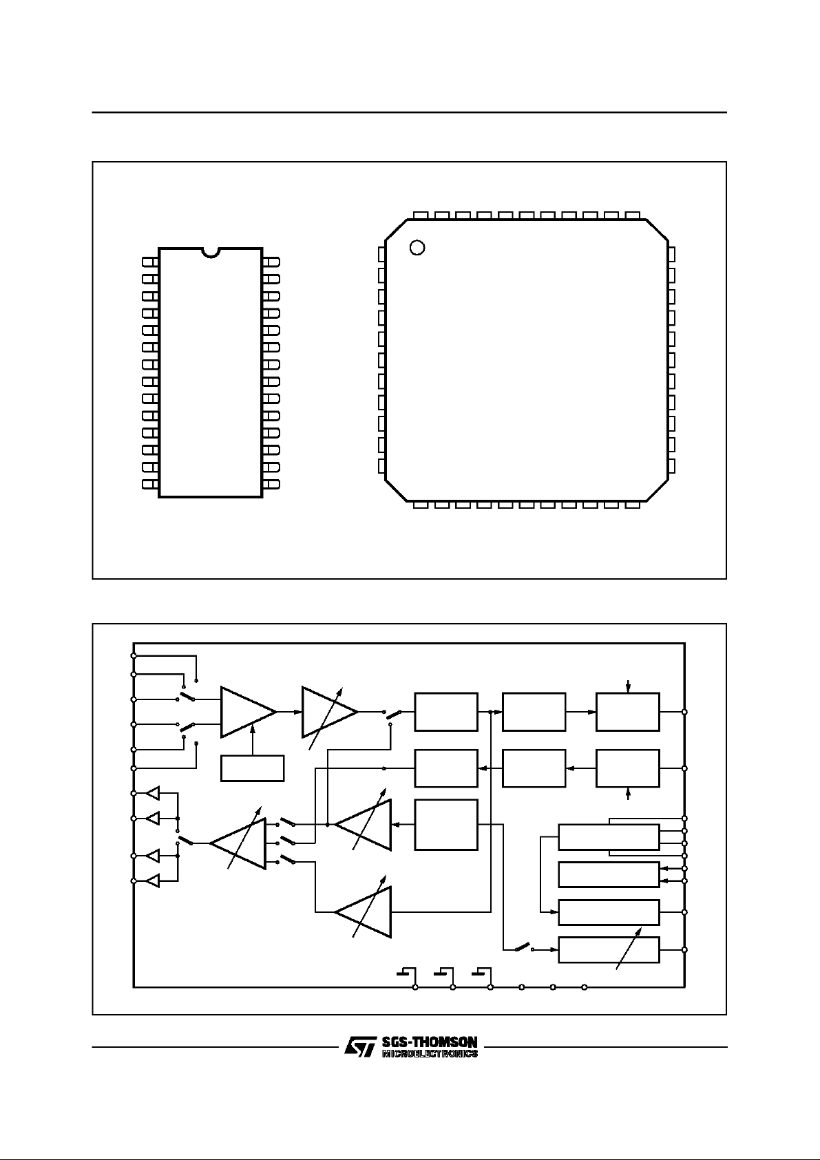
PIN CONNECTIONS(Top view)
N.C.
N.C.
VCCP
VCCA
44 43 42 41 3940 38 37 36 35 34
N.C.
N.C.
MIC3+
MIC3-
GNDA
N.C.
MIC1+
N.C.
V
CCA
V
CCP
N.C.
V
Fr-
V
Fr+
V
Lr-
V
Lr+
GNDP MCLK
D
2
3
4
5
6
SO28
7
8
9
10
R
CCLK
CS-
CI CO
12
13
28
27
26
25
24
23
22
21
20
19
18
17
16
1514BZ V
D94TL094
BLOCKDIAGRAM
MIC3+1
MIC3GNDA
MIC1+
MIC1MIC2+
MIC2LO
FS
GND11
D
x
CC
N.C.
VFr-
VFr+
N.C.
VLr-
VLr+
N.C.
GNDP
N.C.
DR
N.C.
1
2
3
4
5
6
7
8
9
10
12 13 14 15 16
N.C.
N.C.
CCLK
TQFP44
171118 19 20 21 22
CI
CS-
BZ
VCC
CO
DX
GND
N.C.
33
32
31
30
29
28
27
26
25
24
23
MIC1-
N.C.
MIC2+
MIC2-
N.C.
N.C.
N.C.
LO
MCLK
FS
N.C.
D94TL095
2/29
MIC3-
MIC2-
MIC1-
MIC2+
MIC1+
MIC3+
VFr-
VFr+
VLr-
VLr+
EARA OUTPUT
-1
12dB
1
OE
-1
12dB
1
EXTA OUTPUT
MIC
PREAMP
20dB
+ MUTE
VS & TE
0 -> -30dB,
2dB STEP
RTE
SE
SI
D93 TL074
MIC
AMP
0 -> 22.5
1.5dB STEP
TONE
0 -> -27dB
3dB STEP
SIDETONE
-12.5 -> -27.5dB
1dB STEP
AMP
PREFILTER &
DE
(A)
(B)
AMP
BANDPASS
FILTER
BANDPASS
FILTER
TONE, RING
& DTMF
GENER.
& FILTER
GNDP GNDA GND VCCA VCC VCCP
PCM ADC
PCM DAC
CONTROL INTERFACE
CLOCK GENERATOR
BE
EN
TRANSMIT
REGISTER
RECEIVE
REGISTER
EN
µ-WIRE
& SYNCHRONIZER
INTERFACE LATCH
BUZZER
DRIVER
LEVEL
(PWM)
DX
DR
CO
CI
CSCCLK
MCLK
FS
LO
BZ
ADJUST
Page 3

PIN FUNCTIONS (SO28)
Pin Name Description
1 N.C. Not Connected.
2V
3V
4 N.C. Not Connected.
5,6 V
7,8 V
Fr+,VFr–
Lr+,VLr–
9 GNDP Power ground. V
10 D
11 CCLK Control Clock input: This clock shifts serial control information into CI and out from CO when the
12 CS- Chip Select input: When thispin is low, control information is writteninto and out from theST5090
13 CI Control data Input: Serial Control information isshifted into the ST5090 on this pin when CS- is low
14 BZ Pulse width modulated buzzer driver output.
15 V
16 CO Control data Output: Serialcontrol/status information is shifted out from the ST5090 on thispin
17 D
18 GND Ground: All digitalsignals are referenced to this pin.
19 FS Frame Sync input: This signal is a 8kHz clock which defines the start of the transmit and receive
20 MCLK Master ClockInput:Thissignalisusedbythe switchedcapacitor filtersandthe encoder/decoder
21 LO A logic1 written into DO (CR1) appears atLO pin as a logic 0
22 MIC2- Second negative high impedance input to transmit pre-amplifier formicrophoneconnection.
23 MIC2+ SecondPositive high impedance input to transmitpre-amplifier for microphone connection.
24 MIC1- Negative highimpedance inputtotransmitpre-amplifier formicrophone connection.
25 MIC1+ Positivehighimpedance input to transmit pre-amplifier for microphone connection.
26 GNDA Analog Ground: All analog signals are referenced to this pin. GND and GNDA must be connected
27 MIC3- Thirdnegative high impedance output to transmitpreamplifier formicrophone connection.
28 MIC3+ Third positive high impedance output to transmit preamplifier for microphone connection.
Positive power supply inputfor the analogsection.
CCA
+5V ±10% or 3.3V ±10% selec table. V
Positive power supply inputfor the powersection. 5V ±10% or 3.3V ±10% selectable V
CCP
V
must be connected together.
CC
CC
and V
must be direct ly c on nect ed toget h er .
CCA
Receiveanalog earpiece amplifier complementary outputs.These outputscandrive directlyearpiece
transductor. The signalat thisoutputcan bethesum of:
- Receive Speech signal from D
,
R
- Internal Tone Generator,
- Sidetone signal.
Receive analog extra amplifier complementary outputs. The signal at these outputs can bethe
sum of:
- Receive Speech signal from D
,
R
- Internal Tone generator,
- Sidetone signal.
and VLrdriver are referenced to this pin. GNDP and GND must be connected
Fr
together close to the device.
Receivedata input: Data isshifted in during the assigned Received timeslots Indelayedand non-
R
delayed normal frame synchr.modes voice databyte is shiftedin at the MCLK frequencyon the
fallingedges of MCLK, whilein non-delayed reverseframesynchr.mode voicedata byte isshiftedin
at the MCLK frequency onthe rising edges ofMCLK.
CS- input is low, depending on the currentinstruction. CCLK may beasynchronous with the other
system clocks.
via CI andCO pins.
on the rising edges of CCLK.
Positive power supply inputfor the digitalsection. +5V ±10% or 3.3V ±10% selectable.
CC
when CS- islow on the fallingedges of CCLK.
Transmit Data ouput: Data is shifted out onthis pinduring the assigned transmit timeslots.
X
Elsewhere D
synchr. modes, voicedata byte is shiftedout from TRISTATE output D
output is in the high impedance state.In delayed and non-delayed normal frame
X
at the MCLK on the rising
X
edge of MCLK, while in non-delayed reverse frame synchr mode voice data byte isshifted outon
the falling edge of MCLK.
frames. Any ofthree formats may be used forthis signal: non delayed normal mode, delayed
mode, and nondelayed reverse mode.
sequencinglogic.Valuesmustbe512 kHz, 1.536MHz, 2.048MHz or2.56MHz selectedbymeans of
ControlRegister CRO. MCLKisusedalsoto shift-inandout data.
A logic 0 written into DO (CR1) appears at LO pinas a logic 1.
together close to the device.
CCP
ST5090
and
3/29
Page 4

ST5090
PIN FUNCTIONS (TQFP44)
Pin Name Description
1 N.C. Not Connected.
2,3 V
Fr+,VFr–
4 N.C. Not Connected.
5,6 V
Lr+,VLr–
7 N.C. Not Connected.
8 GNDP Power ground. V
9 N.C. Not Connected.
10 D
11,12,13 N.C. Not Connected.
14 CCLK Control Clock input: This clock shifts serial control information into CI and out from CO when the
15 CS- Chip Select input: When thispin is low, control information is writteninto and out from theST5090
16 CI Control data Input: Serial Control information isshifted into the ST5090 on this pin when CS- is low
17 BZ Pulse width modulated buzzer driver output.
18 V
19 CO Control data Output: Serialcontrol/status information is shifted out from the ST5090 on thispin
20 D
21 GND Ground: All digitalsignals are referenced to this pin.
22,23 N.C. Not Connected.
24 FS Frame Sync input: This signal is a 8kHz clock which defines the start ofthe transmitand receive
25 MCLK Master ClockInput:Thissignalisusedbythe switchedcapacitor filtersand the encoder/decoder
26 LO A logic1 written into DO (CR1) appears at LO pin as a logic 0
27,28,29 N.C. Not Connected.
30 MIC2- Second negative high impedance input to transmit pre-amplifierfor microphone connection.
31 MIC2+ SecondPositive high impedance input to transmitpre-amplifier for microphone connection.
32 N.C. Not Connected.
33 MIC1- Negative highimpedance inputtotransmitpre-amplifier formicrophone connection.
34 MIC1+ Positivehighimpedance input to transmit pre-amplifier formicrophone connection.
35 N.C. Not Connected.
36 GNDA Analog Ground: Allanalog signals are referenced to this pin. GND and GNDA must be connected
37 MIC3- Thirdnegative high impedance output to transmitpreamplifier for microphone connection.
38 MIC3+ Third positive high impedance output to transmit preamplifier for microphone connection.
39,40 N.C. Not Connected.
41 V
42 V
43,44 N.C. Not Connected.
Receiveanalog earpiece amplifier complementary outputs.These outputscandrive directlyearpiece
transductor. The signalat thisoutputcan bethesumm of:
- Receive Speech signal from D
,
R
- Internal Tone Generator,
- Sidetone signal.
Receiveanalog extra amplifiercomplementary outputs. The signal at theseoutputs can bethe sumof:
- Receive Speech signal from DR,
- Internal Tone generator,
- Sidetone signal.
and VLrdriver are referenced to this pin. GNDP and GND must be connected
Fr
together close to the device.
Receive data input: Datais shifted in during the assigned Received time slots In delayed and non-
R
delayed normal frame synchr.modes voice data byte is shifted in at the MCLK frequency on the
falling edges of MCLK, while in non-delayed reverse framesinchr. mode voice data byte is shifted
in at the MCLK frequency on the risingedges ofMCLK.
CS- input is low, depending on the currentinstruction. CCLK may beasynchronous with the other
system clocks.
via CI andCO pins.
on the rising edges of CCLK.
Positive power supply inputfor the digitalsection. +5V ±10% or 3.3V ±10% selectable.
CC
when CS- islow on the fallingedges of CCLK.
TransmitDataouput: Data is shiftedoutonthispinduring theassignedtransmittime slots.Elsewhere
X
D
outputis inthe highimpendance state.In delayed and non-delayed normalframesynchr. modes,
X
voicedatabyteisshiftedout from TRISTATEoutputD
atthe MCLK on the rising edgeof MCLK,while
X
innon-delayed reverseframesynchr mode voicedatabyte is shiftedout on the falling edgeof MCLK.
frames. Either of three formats may be used for this signal: non delayed normal mode, delayed
mode, and nondelayed reverse mode.
sequencinglogic.Valuesmustbe512 kHz, 1.536MHz, 2.048MHzor2.56MHzselectedbymeans of
ControlRegister CRO. MCLKisusedalsoto shift-inand out data.
A logic 0 written into DO (CR1) appears at LO pinas a logic 1.
together close to the device.
Positive power supply inputfor the analogsection.
CCA
+5V ±10% or 3.3V ±10% selec table. V
Positive power supply inputfor the powersection. 5V ±10% or 3.3V ±10% selectable V
CCP
V
must be connected together.
CC
CC
and V
must be direct ly c on nect ed toget h er .
CCA
CCP
and
4/29
Page 5

ST5090
FUNCTIONAL DESCRIPTION
IDEVICE OPERATION
I.1 Poweron initialization:
When power is first applied, power on reset circuitry initializes ST5090 and puts it into the power
down state. GainControl Registersfor the various
programmable gain amplifiers and programmable
switches are initialized as indicated in the Control
Registerdescription section. AllCODEC functions
are disabled.
The desired selection for all programmable functions may be intialized prior to a power up commandusing theMICROWIREcontrol channel.
I.2 Powerup/down control:
Following power-on initialization, power up and
power down controlmay be accomplishedby writing any of thecontrol instructions listed in Table 1
into ST5090 with ”P” bit set to0 for power up or1
for power down.
Normally, it is recommendedthat all programmable functions be initially programmed while the
device is powered down. Power state control can
then be included with the last programming instructionor in a separatesingle byte instruction.
Any of the programmable registers may also be
modified while ST5090 is powered up or down by
setting ”P” bit as indicated. When power up or
down control is entered as a single byte instruction, bit 1 must be set toa 0.
When a power up command is given, all de-activated circuits are activated, but output D
will re-
X
main in the highimpedance state until the second
Fs pulse afterpower up.
I.3 Powerdown state:
Following a period of activity, power down state
may be reentered by writing a power down instruction.
Control Registersremain in their current stateand
can be changed by MICROWIRE control interface.
In addition to the power down instruction, detection of loss MCLK (no transition detected) automatically enters the device in ”reset” power down
statewith D
outputin the high impedance state.
X
I.4 Transmit section:
Transmit analog interface is designed in two
stages to enable gains up to 42.5 dB to be realized. Stage 1 is a low noise differential amplifier
providing 20 dB gain. A microphone may be capacitevely connected to MIC1+, MIC1- inputs,
while the MIC2+ MIC2– and MIC3+ MIC3- inputs
may be used to capacitivelyconnect a second microphone or a third microphone respectively or an
auxiliary audio circuit. MIC1 or MIC2 or MC3 or
transmit mute is selected with bits 6 and 7 of registerCR4.
In the mute case, the analog transmit signal is
grounded and the sidetone path is also disabled.
Following the first stage is a programmable gain
amplifier which provides from 0 to 22.5 dB of additional gain in 1.5dB step. The total transmit gain
should be adjusted so that, at reference point A,
see Block Diagram description, the internal 0
dBm0 voltage is 0.49 Vrms (overload level is 0.7
Vrms). Second stage amplifier gain can be programmed with bits 4 to 7 ofCR5.
An activeRC prefilterthen precedesthe 8th order
band pass switchedcapacitor filter. A/D converter
can be either a 14-bitlinear (bit CM = 0 in register
CR0) or can have a compressing characteristics
(bit CM = 1 in register CR0) accordingto CCITTA
or MU255 coding laws. A precision on chip voltage reference ensures accurate and highly stable
transmissionlevels.
Any offset voltagearising in the gain-setamplifier,
the filtersor the comparatoris cancelledby an internal autozero circuit.
Each encode cycle begins immediatly at the beginning of theselected Transmit time slot. The total signal delay referencedto the start of the time
slot isapproximatively 195 µs (due tothe transmit
filter) plus 125 µs (due to encoding delay), which
totals 320 µs. Voice data is shifted out on D
X
during the selected time slot on the transmit rising
edges of MCLK in delayed or non-delayed normal
mode or on the falling edges of MCLK in non-delayed reverse mode.
I.5Receive section:
Voice Data is shifted into the decoder’s Receive
voice data Register via the D
lected time slot on the falling edges of MCLK in
delayed or non-delayed normal mode or on the
rising edges of MCLK in non-delayed reverse
mode.
The decoder consists of either a 14-bit linear or
an expanding DAC with A or MU255 law decoding characteristic. Following the Decoder is a
3400 Hz 8th order band-pass switched capacitor
filter with integral Sin X/X correction for the8 kHz
sampleand hold.
0 dBmO voltage at this (B) reference point (see
Block Diagram description) is 0.49 Vrms. A transcient suppressing circuitry ensure interference
noise suppression at power up.
The analog speech signal output can be routed
eitherto earpiece(V
tra analog output (V
FR+,VFR-
Lr+,VLr-
bits OE and SE (1 and 0 of CR4).
Total signal delay is approximatively 190µs (filter
plus decoding delay) plus 62.5 µs (1/2 frame)
which gives approximatively252µs.
Differential outputs V
FR+,VFR-
rectly drive an earpiece. Preceding the outputs is
a programmableattenuationamplifier,which must
pin during the se-
R
outputs)or to an ex-
outputs) by setting
are intended to di-
5/29
Page 6

ST5090
be set by writing to bits 4 to 7 in register CR6. Attenuations in the range 0 to -30 dB relative to the
maximum level in 2 dB step can be programmed.
The input of this programmable amplifier is the
sum of several signals which can be selected by
writing to register CR4.:
- Receive speech signal which has been decoded and filtered,
- Internally generated tone signal, (Tone amplitude isprogrammedwith bits 4 to 7 of register
CR7),
- Sidetone signal, the amplitude of which is programmed with bits 0 to3 ofregister CR5
V
FR+
and V
outputsare capableof driving output
FR-
power level up to 66mW into differentially connectedload impedanceof 30Ω. Piezoceramic receivers up to50nF can also be driven.
Differential outputs V
Lr+,VLr-
are intended to directlydrive an extraoutput. Precedingthe outputs
is a programmable attenuation amplifier, which
must be set by writing to bits 0 to 3 in register
CR6. Attenuations in the range 0 to -30 dB relative to the maximum level in 2.0 dB step can be
programmed. The input of this programmable amplifier can be the sumof signals which can be selected by writing to register CR4:
- Receive speech signal which has been decoded and filtered,
- Internally generated tone signal, (Tone amplitude isprogrammedwith bits 4 to 7 of register
CR7),
- Sidetone signal, the amplitude of which is programmed with bits 0 to3 ofregister CR5.
and V
V
Lr+
outputs are capable of driving output
Lr-
power level up to 66mW into differentially connectedload impedance of 30 Ω. Piezoceramic re-
ceivers up to50nF can also be driven.
Non delayed data mode is similar to long frame
timing on ST5080A: first time slot begins nominally coincident with the rising edge of F
. Alter-
S
native is touse delayed data mode, which is similar to short frame sync timing on ST5080A, in
which F
input must be high at least a half cycle
S
of MCLK earlier the frame beginning. In the case
of companded code only (bit CM = 1 in register
CRO) a time slot assignment circuit on chip may
be used with all timing modes, allowing connection to one of the two B1 and B2 voice data channels.
Two data formats are available:in Format 1, time
slot B1 corresponds to the 8 MCLK cycles following immediately the rising edge of FS, while time
slot B2 corresponds to the 8 MCLK cycles following immediatelytime slot B1.
In Format 2, time slot B1 is identical to Format 1.
Time slot B2 appears two bit slots after time slot
B1. This two bits space is left available for insertion of the D channel data.
Data format is selected by bit FF (2) in register
CR0. Time slot B1 or B2 is selected by bit TS (1)
in Control RegisterCR1.
Bit EN (2) in control register CR1 enables or disables the voice data transfer on D
and DRas
X
appropriate. During the assigned time slot, D
output shifts data out from the voicedata register
on the rising edges of MCLK in the case of delayed and non-delayed normal modes or on the
falling edges of MCLK in the case of non-delayed
reverse mode. Serial voice data is shifted into D
input during the same time slot on the falling
edges of MCLK in the case of delayed and nondelayed normal modes or on the rising edges of
MCLK in the caseof non-delayedreverse mode.
D
is in the high impedance Tristate condition
X
when in the non selected time slots.
X
R
BUZZEROUTPUT:
Single ended output BZ is intended to drive a
buzzer, via an external BJT, with a squarewave
pulse width modulated (PWM) signal the frequency ofwhich is stored into registerCR8.
For some applications it is also possible to amplitude modulate this PWM signal with a squarewave signal having a frequency stored in register
CR9.
Maximumload for BZ is 5kΩand 50pF.
I.6 DigitalInterface (Fig. 1)
F
Frame Sync input determines the beginning of
S
frame. It may have any durationfrom a single cycle of MCLK to a squarewave. Three different relationships may be established between the
Frame Sync input and the first time slot of frame
by setting bits DM1 and DM0 in register CR1.
6/29
I.7Control Interface:
Control information or data is written into or readback from ST5090 via the serial control port consisting of control clock CCLK, serial data input CI
and output CO, and Chip Select input, CS-. All
controlinstructions require 2 bytesas listed in Table 1, with the exception of a single byte powerup/down command.
To shiftcontrol data into ST5090, CCLK must be
pulsed high 8 times while CS- is low. Data on CI
input is shifted into the serial input register on the
rising edge of each CCLK pulse. After all data is
shifted in, the content of the input shift register is
decoded, and may indicate that a 2nd byte of
control data will follow. This second byte may
either be defined by a second byte-wide CSpulse or may follow the first contiguously, i.e. it is
not mandatory for CS- to return high in between
the first and second control bytes. At the end of
the 2nd control byte, data is loaded into the ap-
Page 7
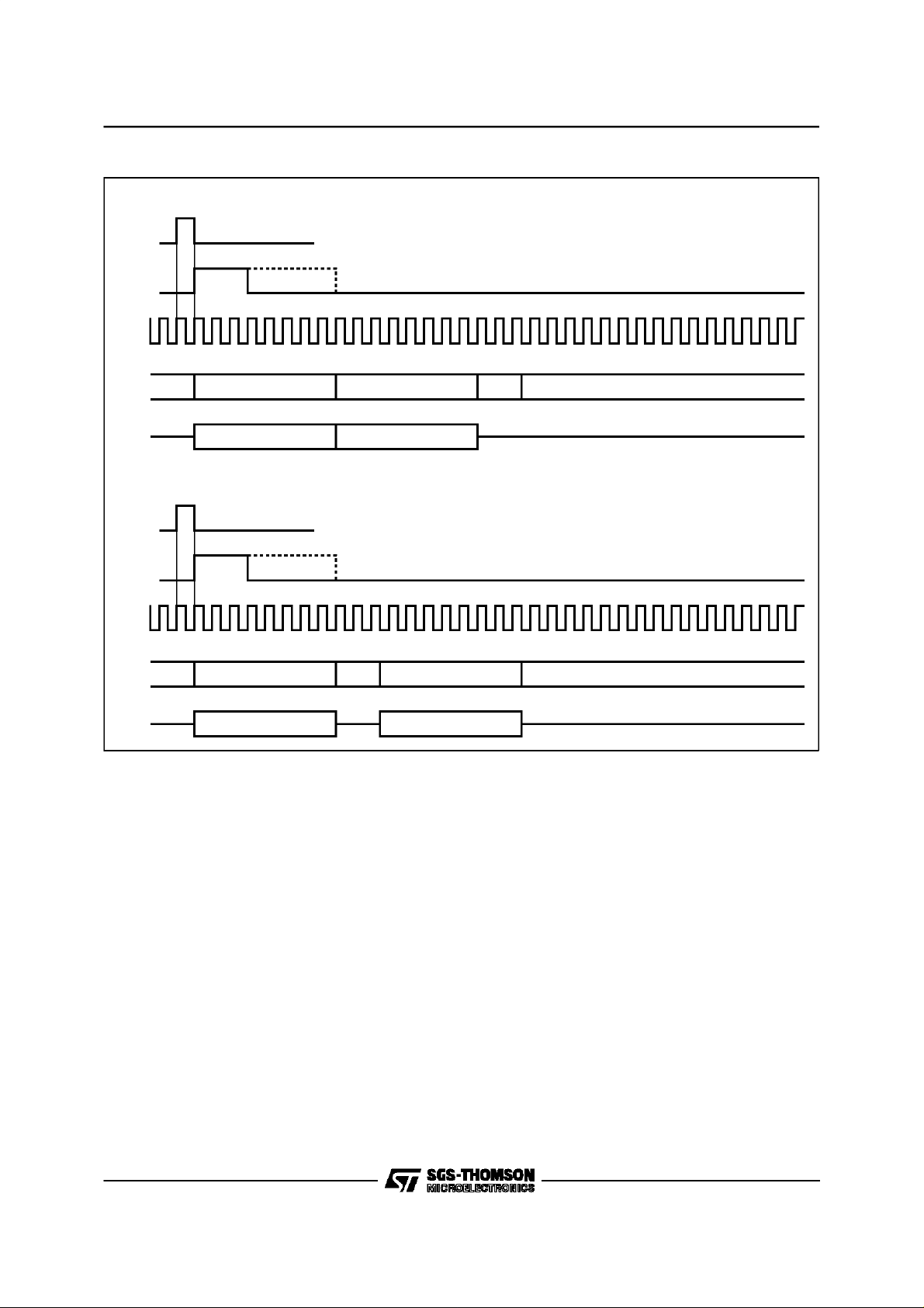
Figure1: Digital InterfaceFormat (*)
FORMAT 1
(delayed timing)F5
ST5090
F6
MCLK
DR
DX
F9
MCLK
DR
DX
FORMAT 2
(non delayed timing)
XB2B1 XX
B2B1
(delayed timing)F8
(non delayed timing)
XB2B1 XX
B2B1
D93TL075
(*) SignificantOnly ForCompanded Code.
propriate programmable register. CS- must return
high at the end of the 2nd byte.
To read-back status information from ST5090,the
first byte of the appropriate instruction is strobed
in during the first CS- pulse, as defined in Table
1. CS- must be set low for a further 8 CCLK cycles, during which data is shifted out of the CO
pin on the fallingedges of CCLK.
When CS- is high, CO pin is in the high impedance Tri-state, enabling CO pins of several devices to be multiplexedtogether.
Thus, to summarise, 2 byte READ and WRITE instructions may use either two 8-bit wide CSpulsesor a single16 bit wide CS- pulse.
I.8 Control channel access toPCM interface:
It is possible to access the B channel previously
selected in Register CR1 in the case of companded code only.
A byte written into Control Register CR3 will be
automatically transmitted from D
output in the
X
following frame in placeof the transmitPCMdata.
A byte written into Control Register CR2 will be
automatically sent through the receivepath to the
Receive amplifiers.
In orderto implementa continuous data flow from
the Control MICROWIRE interface to a B channel, it is necessary to send the control byte on
each PCM frame.
A current byte received on D
input can be read
R
in the register CR2. In order to implement a continuous data flow from a B channel to MICROWIRE interface,it is necessary to read register CR2 at each PCM frame.
7/29
Page 8

ST5090
IIPROGRAMMABLE FUNCTIONS
For both formats of Digital Interface, programmable functions are configured by writing to a number of registersusing a 2-byte write cycle.
verification. Byte one is always register address,
while byte two isData.
Table 1 lists the register set and their respective
adresses.
Most of theseregisters can also be read-back for
Table 1: ProgrammableRegister Intructions
Function Address byte
76543210
Single byte Power up/down P X X X X X 0 X none
Write CR0 P 000001XseeCR0TABLE 2
Read-back CR0 P 0 0 0 0 1 1 X see CR0
Write CR1 P 000101XseeCR1TABLE 3
Read-back CR1 P 0 0 0 1 1 1 X see CR1
Write Data to receive path P 001001XseeCR2TABLE 4
Read datafrom D
Write Data to D
Write CR4 P 010001XseeCR4TABLE 6
Read-back CR4 P 0 1 0 0 1 1 X see CR4
Write CR5 P 010101XseeCR5TABLE 7
Read-back CR5 P 0 1 0 1 1 1 X see CR5
Write CR6 P 011001XseeCR6TABLE 8
Read-back CR6 P 0 1 1 0 1 1 X see CR6
Write CR7 P 011101XseeCR7TABLE 9
Read-back CR7 P 0 1 1 1 1 1 X see CR7
Write CR8 P 100001XseeCR8TABLE 10
Read-back CR8 P 1 0 0 0 1 1 X see CR8
Write CR9 P 100101XseeCR9TABLE 11
Read-back CR9 P 1 0 0 1 1 1 X see CR9
Write CR10 P 101001XseeCR10 TABLE 12
Read-back CR10 P 1 0 1 0 1 1 X see CR10
Write CR11 P 101101XseeCR11 TABLE 13
Read-back CR11 P 1 0 1 1 1 1 X see CR11
Write Test Register CR14 P 111001Xreserved
R
X
P001011XseeCR2
P001101XseeCR3TABLE 5
Data byte
NOTE 1: bit 7 ofthe addressbyte and data byteis always the firstbit clocked into orout from:CI and CO pins when MICROWIREserial
NOTE 2: ”P” bit isPower up/downControl bit. P = 1 MeansPower Down.
NOTE 3: Bit 2 is write/read selectbit.
NOTE 4: RegistersCR12, CR13, and CR15 are not accessible.
8/29
port isenabled.
X =reserved: write0
Bit 1 indicates, if set,the presence of a second byte.
Page 9
Table 2: ControlRegister CR0Functions
ST5090
76543210
F1 F0 CM MA IA FF B7 DL
0
0
1
0
0
1
1
1
0
1
0
0
1
0
0
1
1
1
0
1
0
1
*: state at power on initialization
(1): significantin companded mode only
MCLK = 512 kHz
MCLK = 1.536 MHz
MCLK = 2.048 MHz
MCLK = 2.560 MHz
Linear code
Companded code
Linear Code Companded Code
2-complement *
sign and magnitude
2-complement
1-complement
B1 and B2 consecutive
B1 and B2 separated
8 bitstime-slot
7 bitstime-slot
01Normaloperation
Digital Loop-back
Function
*
*
MU-law: CCITT D3-D4 *
MU-law: Bare Coding
A-law including even bit inversion
A-law: Bare Coding
* (1)
(1)
* (1)
(1)
*
Table 3: ControlRegister CR1 Functions
76543210
DM1 DM0 DO MR MX EN TS SV
X
0
0
1
1
1
0
1
0
1
0
1
0
1
0
1
*: state at power on initialization
(1): significant in companded mode only
delayed data timing
non-delayed normal data timing
non-delayed reverse data timing
L0 latch set to 1
L0 latch set to 0
D
connected to rec. path
R
CR2 connected to rec. path
Trans path connected to D
CR3 connected to D
X
voice data transfer disable
voice data transfer enable
B1 channel selected
B2 channel selected
013.3V power supply
5.0V power supply
Function
X
*
*
*
(1)
*
(1)
*
* (1)
(1)
*
9/29
Page 10

ST5090
Table 4: Control Register CR2 Functions
76543210
d7 d6 d5 d4 d3 d2 d1 d0
Function
msb lsb Data sent to Receive path or Data receivedfrom D
(1) Significant in companded mode only.
Table 5: ControlRegisters CR3 Functions
76543210
d7 d6 d5 d4 d3 d2 d1 d0
msb lsb D
(1) Significant in companded mode only
data transmitted (1)
X
Function
Table 6: ControlRegister CR4 Functions
76543210
VS TE SI OE1 OE2 RTE SE
0
0
1
0
0
1
1
1
0
1
0
0
1
0
0
1
1
1
0
1
X
01Receive Signal to V
Transmit input muted
MIC1 Selected
MIC2 Selected
MIC3 Selected
Internal sidetone disabled
Internal sidetone enabled
Receive output muted
VFr output selected
VLr output selected
NOT ALLOWED
Ring / Tone to V
Ring/ Tone to V
Receive Signal to V
or VLrdisabled
Fr
or VLrenabled
Fr
Fr
Fr
Function
or VLrdisabled
or VLrenabled
input (1)
R
*
*
*
*
*
*: state at power on initialization
X: reserved: write 0
10/29
Page 11

Table 7: ControlRegister CR5Functions
ST5090
76543210
Transmit amplifier Sidetone amplifier
0
0
0
-
1
1
*:state atpower on initialization
1
0
-
1
1
0
0
0
0
-
1
0
0
-
1
1
0
0
0
Table 8: ControlRegister CR6Functions
76543210
Earpiece ampifier
[EARA]
0
0
0
0
-
1
*:state atpower on initialization
0
0
-
1
1
Extra amplifier [EXTA]
0
1
-
1
0
0
0
0
-
1
1
0
0
-
1
0 dBgain
1.5dB gain
in 1.5 dB step
22.5 dB gain
-12.5 dB gain
0
-13.5 dB gain
1
in 1 dB step
-
-27.5 dB gain
1
0 dBgain
-2dB gain
in 2 dB step
-30 dB gain
0 dBgain
0
-2dB gain
1
in 2 dB step
-
-30 dB gain
1
Function
*
*
Function
*
*
Table 9: ControlRegister CR7Functions
76543210 Function
Tone gain F1 F2 SN DE Attenuation f1 V
0
0
0
0
0
0
0
1
0
1
0
1
0
1
0
X
1
X
1
1
0
0
1
1
1
0
0
1
0
0
1
1
1
0
X
1
X
0
0
1
0
0
1
1
1
0
0
0
0
1
*: state at power on initialization
(2): value provided if f1 or f2 is selected alone.
X reserved: write 0
if f1 and f2 are selected in the summed mode, f1=0.89V
01Normal operation
....0dB *
-3 dB
-6 dB
-9dB
-12 dB
-15 dB
-18 dB
-21 dB
-24 dB
-27 dB
f1 and f2 muted
f2 selected
f1 selected
f1 and f2 in summed mode
Squarewave signal selected
Sinewave signal selected
Tone / Ring Generator connected to
Transmit path
while f2=0.7 Vpp.
pp
pp
...1.6(2)
0.066
f2 V
pp
1.26(2)
0.053
*
*
*
11/29
Page 12

ST5090
Table 10: Control Register CR8 Functions
76543210
f17 f16 f15 f14 f13 f12 f11 f10
msb lsb Binary equivalent of the decimal number used to calculate f1
Function
Table 11: Control Register CR9 Functions
76543210
f27 f26 f25 f24 f23 f22 f21 f20
msb lsb Binary equivalent of the decimal number used to calculate f2
Function
Table 12: Control Register CR10 Functions
76543210
DFT HFT
XXXXXX
0
0
1
1
(*) Defaultvalues inserted into the Register at PowerOn.
(*)Standard FrequencyTone Range
0
Halved Frequency Tone Range
1
DoubledFrequency Tone Range
0
Forbidden
1
Function
X reserved, write 0.
Table 13: Control Register CR11 Functions
76543210
BE BI BZ5 BZ4 BZ3 BZ2 BZ1 BZ0
0
1
0
1
msb lsb Binary equivalent of the decimal number used to calculate the
* state at power on initialization
12/29
Function
Buzzer output disabled (set to 0) *
Buzzer output enabled
Duty Cycle isintended as the relative width of logic 1 *
Duty cycle isintended as the relative widthof logic 0
duty cycle.
Page 13

ST5090
CONTROLREGISTERCR0
First byte of a READ or a WRITE instruction to
Control Register CR0 is as shown in TABLE 1.
Secondbyte isas shown in TABLE2.
Master Clock FrequencySelection
A master clock must be provided to ST5090 for
operationof filter and coding/decoding functions.
MCLK frequency can be either 512 kHz, 1.536
MHz,2.048 MHz or 2.56 MHz.
Bit F1 (7) and F0 (6) must be set during initialization to selectthe correct internal divider.
Defaultvalue is512 kHz.
Any clock different from the default one must be
selectedprior a Power-Up instruction.
Coding LawSelection
Bits MA (4) and IA (3) permitselection of Mu-255
law or A law coding with or without even bit inversion if companded code (bit CM = 1) is selected.
Bits MA(4) and IA(3) permit selection of 2-complement, 1-complement or sign and magnitude if
linear code (bit CM= 0) is selected.
CodingSelection
Bit CM (5) permitsselectioneither of linear coding
(14-bit) or companded coding (8-bit). Default
value is linearcoding.
DigitalInterface format (1)
Bit FF(2) = 0 selects digital interface in Format 1
where B1 and B2 channel are consecutive. FF=1
selects Format 2 where B1 and B2 channel are
separated by two bits. (See digital interface format section.)
56+8 selection (1)
Bit ’B7’ (1) selects capability for ST5090 to take
into account only the seven most significant bits
of the PCMdata byte selected.
When ’B7’ is set, the LSBbit on D
LSB bit on D
ishigh impedance.This functional-
X
is ignoredand
R
lows connection of an external ”in band” data
generator directly connected on the Digital Interface.
Digital loopback
Digital loopback mode is entered by setting DL
bit(0) equal 1.
In Digital Loopback mode, data written into Receive PCM Data Register from the selected received time-slot is read-back from that Register in
the selected transmittime-slot on D
.
X
No PCM decoding or encoding takes place in this
mode. Transmit and Receive amplifier stages are
muted.
CONTROLREGISTER CR1
First byte of a READ or a WRITE instruction to
Control Register CR1 is as shown in TABLE 1.
Second byte is as shownin TABLE 3.
Digital InterfaceTiming
Bit DM1(7) = 0 selects digital interface in delayed
timing mode, while DM1= 1 and DM0 = 0 selects
non-delayed normal data timing mode, and DM1
= 1 and DM0 = 1 selects non-delayed reverse
data timing mode.
Default is delayed datatiming.
Latch output control
Bit DO controls directly logical status of latch output LO: ie, a ”ZERO” written in bit DO puts the
output LO at logical 1, while a ”ONE” writtenin bit
DO sets the outputLO to zero.
Microwire access to B channel on receive
path (1)
Bit MR (4) selects access from MICROWIRE
Register CR2 to Receive path. When bit MR is
set high, data written to register CR2 is decoded
each frame, sent to the receive path and data inputat D
is ignored.
R
In the other direction, current PCM data input received at D
can be read from registerCR2 each
R
frame.
Microwire access to B channel on transmit
path (1)
Bit MX (3) selectsaccess from MICROWIREwrite
only Register CR3 to D
set high, data written to CR3is output at D
output. When bit MX is
X
X
every
frame and the output of PCM encoder isignored.
(1) Significant in companded mode only
Mu 255 law
msb lsb msb lsb msb lsb
Vin = + fullscale 100000001010101011111111
Vin = 0 V
Vin = - full scale 000000000010101001111111
MSB is always the first PCM bit shiftedin or outof: ST5090.
10111111111111111011001100110011100000000000000
True A law even bit
inversion
A law without even bit
inversion
0
13/29
Page 14

ST5090
Transmit/Receiveenabling/disabling
Bit ’EN’ (2) enables or disables voice data transfer on D
and DRpins. When disabled, PCM data
X
from DR is not decoded and PCM time-slots are
high impedanceon D
. Defaultvalue is disabled.
X
B-channelselection (1)
Bit TS(1) permits selection between B1 or B2
channels.Default value is B1 channel.
SupplyVoltage selection
Bit SV(0) permits selectionof the power supply of
the ST5090.Default value is 3.3V.
CONTROLREGISTERCR2 (1)
Data sent to receive path or data received from
D
input. Refer to bit MR(4) in ”Control Register
R
CR1” paragraph.
CONTROLREGISTERCR3 (1)
data transmitted.Refer to bit MX(3)in ”Control
D
X
RegisterCR1” paragraph.
CONTROLREGISTERCR4
First byte of a READ or a WRITE instruction to
Control Register CR4 is as shown in TABLE 1.
Secondbyte isas shown in TABLE6.
Transmit Input Selection
MIC1 or MIC2 or MIC3 or transmit mute can be
selectedwith bits 6 and7 (V
and TE).
S
Transmit gain can be adjusted within a 22.5 dB
range in 1.5 dBstep with Register CR5.
SidetoneSelection
Bit ”SI” (5) enables or disables Sidetone circuitry.
When enabled, sidetone gain can be adjusted
with Register (CR5). When Transmit path is disabled, sidetonecircuit is also disabled.
PCM receive dataselection
Bits ”SE” (0) provide select capability to connect
received speech signal either to an extra amplifier
input or to earpieceamplifier input.
CONTROLREGISTER CR5
First byte of a READ or a WRITE instuction to
Control Register CR5 is as shown in TABLE 1.
Second byte is as shownin TABLE 7.
Transmit gainselection
Transmit amplifier can be programmedfor a gain
from 0dB to 22.5dBin 1.5dBstep with bits 4 to 7.
0 dBmO level at the output of the transmit amplifier (A reference point) is 0.492 Vrms (overload
voltage is 0.707 Vrms).
Sidetoneattenuation selection
Transmit signal picked up after the switched capacitor low pass filter may be fed back into both
Receive amplifiers.
Attenuation o f the signal at the output o f the
sidetone attenuator can be programmed from
–12.5dB to -27.5dBrelative to reference point
A in 1 dB step with bits 0 to 3.
CONTROLREGISTER CR6
First byte of a READ or a WRITE instruction to
Control Register CR6 is as shown in TABLE 1.
Second byte is as shownin TABLE 8.
Earpiece amplifiergain selection:
Earpiece Receive gain can be programmed in 2
dB step from 0 dB to -30 dB relative to the maximum with bits 4 to7.
0 dBmO voltage at the output of the amplifier on
pins V
Fr+
andV
is then 1.965 Vrms when 0dB
Fr-
gain is selected down to 61.85 Vrms when -30dB
gain is selected.
OutputDriver Selection
Bits OE1(4) and OE2(3) provide the selection
among the earpiece output or the extra amplifier
output or both outputs muted.
OE1= 1 andOE2 = 1 is notallowed.
Ring/Tonesignal selection
Bit RTE (2) provide select capability to connect
on-chip Ring/Tone generator either to an extra
amplifierinput orto earpiece amplifier input.
(1) Significant in companded mode only
14/29
Extra amplifiergain selection:
Extra Receive amplifier gain can be programmed
in 2 dB step from 0 dB to -30 dB relative to the
maximum with bits0 to3.
0 dBmO voltage on the output of the amplifier on
pins V
Lr+
and V
1.965 Vrms when 0 dB gain is
Lr-
selecteddown to 61.85 mVrms when -30 dB gain
is selected.
CONTROLREGISTER CR7:
First byte of a READ or a WRITE instruction to
Control Register CR7 is as shown in TABLE 1.
Secondbyte is as shown in TABLE9.
Page 15

ST5090
Tone/Ringamplifier gain selection
Output level of Ring/Tone generator, before attenuation by programmable attenuator is 1.6Vpkpk when f1 generator is selected alone or
summed with the f2 generator and 1.26 Vpk-pk
when f2 generatoris selected alone.
Selected output level can be attenuated down to
-27 dB by programmable attenutator by setting
bits 4 to 7.
Frequencymode selection
Bits ’F1’ (3) and ’F2’ (2) permit selection of f1
and/or f2 frequency generator according to TABLE 9.
When f1 (or f2) is selected, output of the
Ring/Toneis a squarewave(or a sinewave) signal
at the frequency selected in the CR8 (or CR9)
Register.
When f1 and f2 are selected in summed mode,
output of the Ring/Tone generator is a signal
where f1 and f2 frequencyare summed.
In order to meet DTMF specifications, f2 output
level is attenuatedby 2dB relative to the f1output
level.
Frequencytemporization must be controlled by the
microcontroller.
Waveformselection
Bit ’SN’ (1) selects waveform of the output of the
Ring/Tone generator. Sinewave or squarewave
signal can be selected.
DTMF selection
Bit DE (0) permitsconnection of Ring/Tone/DTMF
generator on the Transmit Data path instead of
the Transmit Amplifier output. Earpiece or extra
receive output feed-back may be provided by
sidetone circuitry by setting bit SI or directly by
setting bit RTE in Register CR4. Loudspeaker
feed-back may be provided directly by setting bit
RTL in RegisterCR4.
CONTROLREGISTERS CR8 AND CR9
First byte of a READ or a WRITE instruction to
Control Register CR8 or CR9 is as shown in TABLE 1. Second byte is respectively as shown in
TABLE10 and11.
If ”standard frequency tone range” is selected,
Tone or Ring signal frequency value is defined by
the formula:
f1 = CR8 /0.128 Hz
and
f2 = CR9 /0.128 Hz
where CR8 and CR9 are decimal equivalents of
the binary values of the CR8 and CR9 registers
respectively.Thus, any frequencybetween 7.8 Hz
and 1992 Hz may be selectedin 7.8 Hzstep.
If ”halved frequency tone range”is selected, Tone
or Ring signal frequency value is defined by the
formula:
f1 = CR8 / 0.256 Hz
and
f2 = CR9 / 0.256 Hz
This any frequency between 3.9Hz and 996Hz
may be selectedin 3.9Hz step.
If ”doubled frequency tone range”is selected,
Tone or Ring signal frequency value is defined by
the formula:
f1 = CR8 / 0.064 Hz
and
f2 = CR9 / 0.064 Hz
Thus any frequency between15.6Hz and 3984Hz
may be selectedin 15.6Hz step.
TABLE 12 gives examples for the main frequenciesusual forTone or Ring generation.
CONTROLREGISTERCR10
Bit DFT(1) and HFT(0) permits the selection
among ”standard frequencytone range” (i.e. from
7.8Hz to 1992Hz in 7.8Hz step), ”halved frequency tone range” (i.e. from 3.9Hz to 996Hz in
3.9Hz step), and ”doubled frequency tone range”
(i.e. from 15.6Hz to 3984Hz in 15.6Hz step) according to the values described in CONTROL
REGISTERCR8 and CR9.
CONTROLREGISTER CR11
Bit BE(7) permits connection of a f1 squarewave
PWM Ring signal, amplitude modulated or not by
a f2 squarewave signal, to buzzer driver output
BZ. Bits BZ5 to BZ0 define the duty cycle of the
PWM squarewave, according to the following formula:
Duty Cycle= CR11(5 ÷ 0)x 0.78125%
where CR11(5 ÷ 0) is the decimal equivalent of
the binary value BZ5÷ BZ0.
When BE = 1, if bits F1 = 1 and F2 = 0 in register CR7, a f1 PWM ring signal is present at the
buzzer output, while if bits F1 = 1 and F2 = 1 in
register CR7 the f1 PWM ring signal is also amplitude modulated by a f2 squarewave frequency. Bit BI (6) allows to chose the logic level
at which the duty cycle is referred: BI = 0 means
that duty cycle is intended as the relative width
of the logic1, while BI = 1 means that duty cycle
is intended as the relative width of the logic 0.
When BE = 0 (or during power down) BZ = 0 if
BI = 0 or BZ = 1 if BI = 1.
15/29
Page 16

ST5090
Table 12: Examples of UsualFrequency Selection (Standardfrequency tone range)
Description f1 value (decimal) Theoretic value (Hz) Typical value (Hz) Error %
Tone 250 Hz
Tone 330 Hz
Tone 425 Hz
Tone 440 Hz
Tone 800 Hz
Tone 1330 Hz
DTMF 697 Hz
DTMF 770 Hz
DTMF 852 Hz
DTMF 941 Hz
DTMF 1209 Hz
DTMF 1336 Hz
DTMF 1477 Hz
DTMF 1633 Hz
SOL
LA
SI
DO
RE
MI flat
MI
FA
FA sharp
SOL
SOL sharp
LA
SI
DO
RE
MI
32
42
54
56
102
170
89
99
109
120
155
171
189
209
50
56
63
67
75
80
84
89
95
100
106
113
126
134
150
169
250
330
425
440
800
1330
697
770
852
941
1209
1336
1477
1633
392
440
494
523.25
587.33
622.25
659.25
698.5
740
784
830.6
880
987.8
1046.5
1174.66
1318.5
250
328.2
421.9
437.5
796.9
1328.1
695.3
773.4
851.6
937.5
1210.9
1335.9
1476.6
1632.8
390.6
437.5
492.2
523.5
586.0
625.0
656.3
695.3
742.2
781.3
828.2
882.9
984.4
1046.9
1171.9
1320.4
.00
–.56
–.73
–.56
–.39
–.14
–.24
+.44
–.05
–.37
+.16
–.01
.00
.00
–.30
–.56
–.34
+.04
–.23
+.45
–.45
–.45
+.30
–.34
–.29
+.33
–.34
+.04
–.23
+.14
16/29
Page 17

TIMING DIAGRAM
NonDelayed Data Timing Mode(Normal) (*)
ST5090
DelayedData Timing Mode (*)
16
16
17
16
16
17
(*) Inthe caseof companded code the timing is applied to 8 bitsinstead of 16 bits (see ST5080A data sheet)
16
16
17/29
Page 18

ST5090
TIMINGDIAGRAM (continued)
NonDelayed Reverse Data TimingMode (*)
MCLK
FS
DX
DR
tHMFR
12345671617
tHMFRtSFMR
tDFD
tDMDR
1234567 16
tSDM tHMDR
1234567 16
tRM tFM tWMM
(*) Inthe caseof companded code the timing is applied to 8 bitsinstead of 16 bits.
tWML
tDMZR
D93TL076A
Serial Control Timing (MICROWIRE MODE)
18/29
Page 19

ST5090
ABSOLUTEMAXIMUM RATINGS
Parameter Value Unit
to GND 7V
V
CC
Voltage at MIC (V
Current at V
Fr
Current at any digital output + 50 mA
Voltage at anydigital input (V
Storage temperature range - 65 to + 150 °C
Lead Temperature (wave soldering,10s) + 260 °C
TIMINGSPECIFICATIONS(unlessotherwisespecifi ed,VCC=3.3V+ 10%or5V± 10%,TA=–30°Cto85°C;
typical characteristicsare specified V
all signals are referencedto GND, see Note5 fortiming definitions)
NOTICE:All timing specificationscan be changed.
MASTERCLOCK TIMING
Symbol Parameter Test Condition Min. Typ. Max. Unit
f
MCLK
t
WMH
t
WML
t
RM
t
FM
≤ 5.5V) VCC+1 to GND -1 V
CC
and V
Lr
≤ 5.5V); limitedat + 50mA VCC+ 1 to GND - 1 V
CC
= 3.3V,TA=25°C;
CC
Frequency of MCLK Selection of frequency is
programmable (see table 2)
+ 100 mA
512
1.536
2.048
2.560
Period of MCLK high Measured from VIHto V
Period of MCLK low Measured from VILto V
Rise Time ofMCLK Measured from VILto V
Fall Time of MCLK Measured from VIHto V
IH
IL
IH
IL
80 ns
80 ns
kHz
MHz
MHz
MHz
30 ns
30 ns
PCM INTERFACETIMING
Symbol Parameter Test Condition Min. Typ. Max. Unit
t
HMF
t
SFM
t
DMD
t
DMZ
t
DFD
t
SDM
t
HMD
t
HMFR
t
SFMR
t
DMDR
t
DMZR
t
HMDR
Hold Time MCLK low to FS low 0 ns
Setup Time, FS high to MCLK
30 ns
low
Delay Time, MCLK highto data
Load = 100 pf 100 ns
valid
Delay Time, MCLK low to DX
10 100 ns
disabled
Delay Time, FS highto data valid Load = 100 pf ;
100 ns
Applies only ifFS riseslater
than MCLK rising edge in Non
Delayed Mode only
Setup Time, DRvalid toMCLK
20 ns
receive edge
Hold Time, MCLK low to D
R
10 ns
invalid
Hold Time MCLK Highto FS low 30 ns
SetupTime,FS hightoMCLKHigh 30 ns
DelayTime,MCLKlowto datavalid Load = 100pF 100 ns
Delay Time, MCLK High toDX
10 100 ns
disabled
Hold Time, MCLK High to D
R
20 ns
invalid
19/29
Page 20

ST5090
SERIALCONTROL PORT TIMING
Symbol Parameter Test Condition Min. Typ. Max. Unit
f
CCLK
t
WCH
t
WCL
t
RC
t
FC
t
HCS
t
SSC
t
SDC
t
HCD
t
DCD
t
DSD
t
DDZ
t
HSC
t
SCS
Note 5: A signal is valid if it is above VIHor below VILand invalid if it is between VILand VIH.
Frequency of CCLK 2.048 MHz
Period of CCLK high Measured from VIHto V
Period of CCLK low Measured from VILto V
Rise Time ofCCLK Measured from VILto V
Fall Time of CCLK Measured from VIHto V
IH
IL
IH
IL
160 ns
160 ns
50 ns
50 ns
HoldTime,CCLKhigh toCS– low 10 ns
SetupTime,CS–lowtoCCLKhigh 50 ns
SetupTime, CI validto CCLK high 50 ns
HoldTime,CCLKhigh toCIinvalid 50 ns
Delay Time, CCLK low toCO
Load = 100 pF 80 ns
data valid
Delay Time, CS–low to CO data
50 ns
valid
Delay Time CS–high or 8th CCLK
10 80 ns
lowto COhigh impedance
whichever comesfirst
Hold Time, 8th CCLKhigh to
100 ns
CS– high
SetupTime,CS– hig hto CCLKhigh 100 ns
For the purpoes ofthis specification the following conditions apply:
a) All input signal aredefined as: V
b) Delay times are measured from the inputs signal valid tothe output signal valid.
c) Setuptimes are measuredfrom the data input valid tothe clock input invalid.
d) Hold times are measured fromthe clock signal valid to thedata input invalid.
= 0.2VCC,VIH= 0.8VCC,tR< 10ns, tF< 10ns.
IL
ELECTRICALCHARACTERISTICS (unlessotherwisespecified,VCC=3.3V+10% or5V ±10%,TA=–-30°C
to85°C; typicalcharacteristicarespecified atV
=3.3V,TA=25°C ; allsignalsarereferencedto GND )
CC
DIGITAL INTERFACES
Symbol Parameter Test Condition Min. Typ. Max. Unit
V
IL
V
IH
V
OL
V
OH
I
IL
I
IH
I
OZ
Input Low Voltage All digital inputs DC
AC
Input High Voltage Alldigital inputs DCAC0.7V
0.8V
Output Low Voltage Alldigital outputs,IL=10µA
Alldigital outputs,I
Output High Voltage Alldigitaloutputs, IL=10µA
Alldigital outputs,I
Input Low Current Any digitalinput,
GND < V
IN<VIL
Input High Current Any digital input,
V
IH<VIN<VCC
Output Current in High
DXand CO -10 10 µA
=2mA
L
=2mA
L
V
CC
V
CC
-10 10 µA
-10 10 µA
CC
CC
-0.1
-0.4
0.3V
0.2V
0.1
0.4
CC
CC
V
V
V
V
V
V
V
V
impedance (Tri-state)
A.C. TESTING INPUT,OUTPUT WAVEFORM
INTPUT/OUTPUT
0.8VCC
0.2VCC
0.7VCC
0.3VCC
TEST POINTS
0.7VCC
0.3VCC
D93TL077
AC Testing: inputs are driven at 0.8VCCfor
a logic ”1”and0.2VCC for a logic”0 ”.
Timing measurements are made at0.7V
CC
for a logic”1”and 0.3VCCfor a logic ”0”.
20/29
Page 21

ANALOGINTERFACES
Symbol Parameter Test Condition Min. Typ. Max. Unit
I
MIC
R
MIC
R
LVFr
C
LVFr
R
OVFr0
V
OSVFr0
R
LvLr
C
LvLr
R
OLVrO
V
OSVLrO
(*) Seeapplication note for VFrand VLrconnections.
Input Leakage GND < V
Input Resistance GND < V
Load Resistance (*) V
Load Capacitance (*) From V
Output Resistance Steady zeroPCM code applied
Differential offset:
Voltage at V
Fr+,VFr-
Load Resistance (*) V
Load Capacitance (*) from V
Output Resistance Steady zeroPCM code applied
Differential offsetVoltage at
V
Lr+,VLr-
MIC<VCC
MIC<VCC
to V
Fr+
Fr-
to V
Fr+
Fr-
to DR; I = + 1mA
Alternating +zero PCM code
applied to DR maximum
receive gain; R
to V
Lr+
Lr-
Lr+
to V
L
Lr-
= 100Ω
to DR; I + 1mA
Alternating +zero PCM code
applied to DR maximum
receive gain; R
=50Ω
L
-100 +100 µA
50 kΩ
30 Ω
50 nF
1.0 Ω
-100 +100 mV
30 Ω
50 nF
1 Ω
–100 +100 mV
ST5090
POWERDISSIPATION
Symbol Parameter Test Condition Min. Typ. Max. Unit
I
CC0
I
CC0
I
CC1
PowerdownCurrent at 3.3V± 10% CCLK,CI = 0.1V;CS= VCC-0.1V 0.5 5 µA
Power down Current at 5V± 10% CCLK,CI= 0.1V;CS = VCC-0.1V 1 10 µA
Power Up Current at 3.3V ±10% V
Lr+,VLr-
and V
Fr+,VFr-
not
710mA
loaded
I
CC1
Power Up Current at 5V ±10% V
Lr+,VLr-
and V
Fr+,VFr-
not
812mA
loaded
TRANSMISSION CHARACTERISTICS (unless otherwise spec ified, V
= –30° Cto85°C; t ypical charact eristic s ar e s pecified at VCC=3.3V,TA=25°C, M IC1/2/3 =
T
A
0
dBm0, DR= –6dBm0 PCM code, f = 1015.625 Hz; all signal are referenced to GND)
= 3.3V + 10% or 5V ±10%,
CC
AMPLITUDE RESPONSE(Maximum, Nominal, and Minimum Levels)
Transmitpath - Absolute levelsat MIC1/ MIC2 / MIC3
Parameter Test Condition Min. Typ. Max. Unit
0 dBm0 level Transmit Amps connectedfor
20dB gain
Overload level 70.71 mV
0 dBm0 level Transmit Amps connectedfor
42.5dB gain
Overload level 5.302 mV
49.26 mV
3.694 mV
RMS
RMS
RMS
RMS
21/29
Page 22

ST5090
TRANSMISSION CHARACTERISTICS (continued)
AMPLITUDE RESPONSE(Maximum, Nominal, and Minimum Levels)
Receivepath - Absolute levels at V
Parameter Test Condition Min. Typ. Max. Unit
0 dBM0 level Receive Amp programmed for
0 dBM0 level Receive Amp programmed for
AMPLITUDE RESPONSE(Maximum, Nominal, and Minimum Levels)
Receivepath - Absolute levels at V
Parameter Test Condition Min. Typ. Max. Unit
0 dBM0 level Receive Amp programmed for
0 dBM0 level Receive Amp programmed for
AMPLITUDE RESPONSE
Transmitpath
Symbol Parameter Test Condition Min. Typ. Max. Unit
G
XA
G
XAG
G
XAT
G
XAV
G
XAF
G
XAL
(*) The limitatfrequencies between 4600Hz and 8000Hz lieson a straightline connecting the two frequencieson a linear (dB)scale versus log
(Hz) scale.
Transmit Gain Absolute
Accuracy
Transmit Gain Variation with
programmed gain
Transmit Gain Variation with
temperature
Transmit Gain Variation with
supply
Transmit Gain Variation with
frequency
Transmit Gain Variation with
signal level
(Differentiallymeasured)
FR
0dB gain
- 30dBattenuation
(Differentiallymeasured)
Lr
0dB gain
- 30dBgain
Transmit Gain Programmed for
maximum.
Measure deviation of Digital
PCM Code from ideal 0dB
PCM code at D
Measure Transmit Gain over
the range from Maximum to
minimum setting.
Calculate the deviation from
the programmed gain relative
to GXA,
i.e. G
AXG=Gactual-Gprog.-GXA
Measured relative to GXA.
min. gain < G
Measured relative to G
GX= Maximum gain
Relative to 1015,625 Hz,
multitone test technique used.
min. gain < G
f = 60Hz
f = 100 Hz
f = 200 Hz
f = 300 Hz
f = 400 Hz to 3000 Hz
f = 3400 Hz
f = 4000 Hz
f = 4600 Hz (*)
f = 8000 Hz (*)
Sinusoidal Test method.
Reference Level = -10 dBm0
V
= -40 dBm0 to +3 dBm0
MIC
V
= -50 dBm0 to -40 dBm0
MIC
V
= -55 dBm0 to -50 dBm0
MIC
X
< Max. gain
X
< Max. gain
X
XA
m0
1.965 V
RMS
61.85 mV
1.965 V
RMS
61.85 mV
-0.5 0.5 dB
-0.5 0.5 dB
-0.1 0.1 dB
-0.1 0.1 dB
dB
dB
dB
dB
dB
dB
dB
dB
dB
dB
dB
dB
-1.5
-0.5
-1.5
-0.5
-0.5
-1.2
-30
-20
-6
0.5
0.5
0.0
-14
-35
-47
0.5
0.5
1.2
RMS
RMS
22/29
Page 23

AMPLITUDE RESPONSE
Receivepath
Symbol Parameter Test Condition Min. Typ. Max. Unit
G
G
G
G
G
G
G
G
G
RAE
RAL
RAGE
RAGL
RAT
RAV
RAF
RAL E
RAL L
Receive Gain Absolute Accuracy Receive gainprogrammed for
maximum
Apply -6 dB
Measure V
PCM code to D
m0
Fr+
Receive Gain Absolute Accuracy Receive gainprogrammed for
maximum
Receive Gain Variation with
programmed gain
Apply -6 dB
Measure V
Measure VFrGain over the
range from Maximum to
PCM code to D
m0
Lr+
minimum setting.
Calculate the deviation from
the programmed gain relative
to GRAE,
i.e.G
RAGE=Gactual-Gprog.-GRAE
Receive Gain Variation with
programmed gain
Measure VLrGain over the
range from Maximum to
minimum setting.
Calculate the deviation from
the programmed gain relative
to GRAL,
i.e.G
RAGL=Gactual-Gprog.-GRAL
Receive Gain Variation with
temperature
Measured relative to GRA. (V
and VFr)
min. gain < GR < Max. gain
Receive Gain Variation with
Supply
Receive Gain Variation with
frequency (V
and VFr)
Lr
Measured relative to GRA. (V
and VFr)
G
= Maximum Gain
R
Relative to 1015,625 Hz,
multitone test technique used.
min. gain < G
< Max. gain
R
f = 60Hz
f = 100Hz
f = 200 Hz
f = 300 Hz
f = 400 Hz to 3000 Hz
f = 3400 Hz
f = 4000 Hz
Receive Gain Variation with
signal level (V
)
Fr
Receive Gain Variation with
signal level (V
)
Lr
Sinusoidal Test Method
Reference Level = –10 dBm0
D
= -40 dBm0 to -3 dBm0
R
D
= -50 dBm0 to -40 dBm0
R
D
= -55 dBm0 to -50 dBm0
R
Sinusoidal Test Method
Reference Level = –10 dBm0
D
= -40 dBm0 to -3 dBm0
R
D
= -50 dBm0 to -40 dBm0
R
D
= -55 dBm0 to -50 dBm0
R
-0.5 0.5 dB
R
-0.5 0.5 dB
R
-0.5 0.5 dB
-0.5 0.5 dB
-0.1 0.1 dB
Lr
-0.1 0.1 dB
Lr
-1.5
-0.5
-1.5
-0.5
-0.5
-1.2
-0.5
-0,5
-1.2
-20
-12
-2
0.5
0.5
0.0
-14
0.5
0.5
1.2
0.5
0.5
1.2
ST5090
dB
dB
dB
dB
dB
dB
dB
dB
dB
dB
dB
dB
dB
23/29
Page 24

ST5090
ENVELOPEDELAY DISTORTION WITHFREQUENCY
Symbol Parameter Test Condition Min. Typ. Max. Unit
DXA Tx Delay, Absolute f = 1600 Hz 320 µs
DXR Tx Delay, Relative f = 500 - 600Hz
f = 600 - 800 Hz
f = 800 - 1000 Hz
f = 1000 - 1600 Hz
f = 1600 - 2600 Hz
f = 2600 - 2800 Hz
f = 2800 - 3000 Hz
DRA Rx Delay, Absolute f = 1600 Hz 280 µs
DRR Rx Delay, Relative f= 500 - 600Hz
f = 600 - 800 Hz
f = 800 - 1000 Hz
f = 1000 - 1600 Hz
f = 1600 - 2600 Hz
f = 2600 - 2800 Hz
f = 2800 - 3000 Hz
290
180
50
20
55
80
180
200
110
50
20
65
100
220
µs
µs
µs
µs
µs
µs
µs
µs
µs
µs
µs
µs
µs
µs
NOISE
Symbol Parameter Test Condition Min. Typ. Max. Unit
NXP Tx Noise, P weighted (up to
35dB)
NRP Rx Noise, A weighted
(max. gain)
NRS Noise, Single Frequency MIC = 0V, Loop-around
PPSRx PSRR, Tx MIC = 0V,
PPSRp PSRR, Rx PCM Code equals PositiveZero,
SOS SpuriousOut-Band signal at
the output
(*) AWeighted
= 0V, DE = 0 -75 -70 dBm0p
V
MIC
Receive PCMcode= PositiveZero
120 150 µVrms
SI =0 and RTE = 0
-50 dBm0
measurament from f = 0 Hz to
100 kHz
V
= 3.3 VDC+50mV
CC
rms
;
30 60 dB
f = 0Hz to 50KHz
V
= 3.3 VDC + 50 mVrms,
CC
f=0Hz-4kHz
f = 4 kHz - 50 kHz
30
30
70
70
DR input setto -6 dBm0 PCM
code
300 - 3400Hz Input PCM Code
applied at DR
4600 Hz - 5600 Hz
5600 Hz - 7600 Hz
7600 Hz - 8400 Hz
-40
-50
-50
(*)
dB
dB
dB
dB
dB
24/29
Page 25

ST5090
DISTORTION
Symbol Parameter Test Condition Min. Typ. Max. Unit
56
50
48
43
38
29
24
15
37.5
28.5
50
48
43
38
29
24
15
50
48
43
38
29
24
15
#
65
56
64
50
61
48
52
43
42
31
26
23
16
13
64
62
53
43
33
28
18
64
62
53
43
33
28
18
-75 -46 dB
dB
dB
dB
dB
dB
dB
dB
dB
dB
dB
dB
dB
dB
dB
dB
dB
dB
dB
dB
dB
dB
dB
S
TDX
(*)
Signal to Total Distortion
(up to 35dB gain)
Sinusoidal Test Method
(measured using linear 300 to
3400 weighting)
Level = 0 dBm0
Typical values are measured with
30.5dB gain
Level = -6 dBm0
Level = -10 dBm0
Level = -20 dBm0
Level = -30 dBm0
Level = -40 dBm0
Level = -45 dBm0
Level = -55 dBm0
S
DFx
Single Frequency Distortion
0 dBm0 input signal -80 -56 dB
transmit
S
TDRE
(*)
Signal to Total Distortion (VFr)
( up to 20dB attenuation)
Sinusoidal Test Method
(measured using linear 300 to
3400 weighting)
Level = -6 dBm0
Typical values are measured with
20dB attenuation.
Level = -10 dBm0
Level = -20 dBm0
Level = -30 dBm0
Level = -40 dBm0
Level = -45 dBm0
Level = -55 dBm0
S
S
DFr
TDRL
(*)
Single Frequency Distortion
receive (V
)
Fr
Signal to Total Distortion (VLr)
(up to 20dB attenuation)
-6 dBm0 input signal -80 -50 dB
Sinusoidal Test Method
(measured using linear 300 to
3400 weighting)
Level = -6 dBm0
Typical values are measured with
20dB attenuation
Level = -10 dBm0
Level = -20 dBm0
Level = -30 dBm0
Level = -40 dBm0
Level = -45 dBm0
Level = -55 dBm0
S
DLr
Single Frequency Distortion
receive (V
)
Lr
-6 dBm0 input signal -80 -50 dB
IMD Intermodulation Loop-around measurement
Voltage at MIC = -10 dBm0
to -27 dBm0, 2 Frequencies in
the range 300 -3400 Hz
(*) The limitcurve shall bedetermined by straight lines joining successive coordinates given in the table.
(#) Lower limitsused during the automatic testing toavoid unrealistic yield loss due to ±2dB imprecision of time-limitednoise measurements.
CROSSTALK
Symbol Parameter Test Condition Min. Typ. Max. Unit
C
Tx-r
Transmit to Receive Transmit Level = 0 dBm0,
f = 300 - 3400 Hz
DR = Quiet PCM Code
C
Tr-x
Receive to Transmit Receive Level= -6 dBm0,
f = 300 - 3400 Hz
MIC = 0V
-100 -65 dB
-80 -65 dB
25/29
Page 26

ST5090
APPLICATIONS
ApplicationNote for MicrophoneConnections
ST5090
ApplicationNote for VFrandVLrConnections
DYNAMIC
RECEIVERS
(32Ω)
VFr+
VFr-
CERAMIC
R
ST5090
VLr+
R
RECEIVERS
(50nF)
VFr+
VFr-
ST5090
VLr+
ST5090
DYNAMIC/CERAMIC
(REVERSIBLE)
VFr+
VFr-
ST5090
R
VLr+
ST5090
RECEIVERS
VLr-
R must be greater than 30Ω
For highercapacitive transducers, lower R values can be used.
VLr-
POWERSUPPLIES
While pins of ST5090 device are well protected
against electrical misuse, it is recommended that
the standard CMOS practise of applying GNDbefore any other connections are made should always be followed. In applications where the
printed circuit card may be plugged into a hot
socket with power and clocks already present, an
extralong ground pinon the connectorshould be
26/29
VLr-
D93TL078A
used.
To minimize noise sources, all ground connec-
tions to each device should meet at a common
point as close as possible to the GND pin in order
to prevent the interaction of ground return currents flowing through a common bus impedance.
A power supply decoupling capacitor of 0.1 µF
should be connected from this common point to
V
as closeas possibleto the devicepins.
CC
Page 27

TQFP44(10 x 10) PACKAGE MECHANICAL DATA
ST5090
DIM.
mm inch
MIN. TYP. MAX. MIN. TYP. MAX.
A 1.60 0.063
A1 0.05 0.15 0.002 0.006
A2 1.35 1.40 1.45 0.053 0.055 0.057
B 0.30 0.37 0.45 0.012 0.014 0.018
C 0.09 0.20 0.004 0.008
D 12.00 0.472
D1 10.00 0.394
D3 8.00 0.315
e 0.80 0.031
E 12.00 0.472
E1 10.00 0.394
E3 8.00 0.315
L 0.45 0.60 0.75 0.018 0.024 0.030
L1 1.00 0.039
K 0°(min.), 3.5°(typ.), 7°(max.)
D
D1
2333
34
B
44
1
e
22
E3D3E1
12
11
E
L1
L
Seating Plane
K
0.10mm
.004
B
A1
A
A2
C
27/29
Page 28

ST5090
SO28 PACKAGE AND MECHANICAL DATA
DIM.
MIN. TYP. MAX. MIN. TYP. MAX.
A 2.65 0.104
a1 0.1 0.3 0.004 0.012
b 0.35 0.49 0.014 0.019
b1 0.23 0.32 0.009 0.013
C 0.5 0.020
c1 45° (typ.)
D 17.7 18.1 0.697 0.713
E 10 10.65 0.394 0.419
e 1.27 0.050
e3 16.51 0.65
F 7.4 7.6 0.291 0.299
L 0.4 1.27 0.016 0.050
S8°(max.)
mm inch
28/29
Page 29

ST5090
Information furnished is believed to be accurate and reliable. However, SGS-THOMSON Microelectronics assumes no responsibility for the
consequences of use of such information nor for any infringementof patents or other rights of third parties which may result from itsuse. No
license is granted by implication or otherwise under any patent or patent rights of SGS-THOMSON Microelectronics. Specifications mentioned in this publication are subject to change without notice. This publication supersedes and replaces all information previously supplied.
SGS-THOMSON Microelectronics products are not authorized for use as critical components in life support devices or systems without express written approval of SGS-THOMSONMicroelectronics.
1996 SGS-THOMSON Microelectronics All Rights Reserved
Australia - Brazil - Canada - France - Germany - Hong Kong -Italy - Japan- Korea - Malaysia - Malta - Morocco - TheNetherlands
Singapore - Spain - Sweden - Switzerland -Taiwan - Thaliand -United Kingdom - U.S.A.
SGS-THOMSON MicroelectronicsGROUP OF COMPANIES
29/29
 Loading...