

Page 1
PROGRAMMABLE AUDIO FRONT END
FOR DIGITAL PHONES AND ISDN TERMINALS
FEATURES:
CompleteCODECandFILTERsystemincluding:
PCM ANALOG TO DIGITAL AND DIGITAL TO
ANALOG CONVERTERS
POWERFUL ANALOG FRONT END CAPABLE TO INTERFACEDIRECTLY:
- MicrophoneDynamic or Electrete
- Earpiecedownto 100Ω orup to150nF
- Loudspeakerdown to 50Ω or Buzzer up to
600nF.
TRANSMITBAND-PASSFILTER
ACTIVERC NOISE FILTER
RECEIVE LOW-PASS FILTER WITH SIN X/X
CORRECTION
MU-LAW OR A-LAW SELECTABLE COM-
PANDING CODER AND DECODER
PRECISIONVOLTAGE REFERENCE
Phones Features:
DUAL SWITCHABLE MICROPHONE AMPLIFIER INPUTS. GAIN PROGRAMMABLE: 15
dB RANGE,1 dB STEP.
LOUDSPEAKERAMPLIFIEROUTPUT.
SWITCHABLE MAXIMUM GAIN: +9dB/+27dB
WITH AUTOMATIC DIGITAL ANTICLIPPING
SYSTEM. aTTENUATION PROGRAMMABLE:
30dB RANGE,2dB STEP.
SEPARATEEARPIECE AMPLIFIEROUTPUT.
ATTENUATION PROGRAMMABLE: 15 dB
RANGE, 1 dB STEP.
AUXILIARY TAPE RECORDER ANALOG INTERFACE:Tx + Rx COMBINEDOUTPUT.
AUXILIARY SWITCHABLE EXTERNAL RING
INPUT (EAIN).
TRANSIENT SUPRESSION SIGNAL DURING
POWERON.
INTERNAL PROGRAMMABLE SIDETONE
CIRCUIT. ATTENUATION PROGRAMMABLE:
15 dB RANGE, 1 dB STEP, INDEPENDENT
FROM Rx CONTROL.
INTERNALRING OR TONE GENERATORINCLUDING DTMF TONES, SINEWAVE OR
SQUAREWAVE WAVEFORMS. ATTENUATION PROGRAMMABLE: 27 dB RANGE, 3
dB STEP.
RINGER CONTROL PROGRAMMABLE IN-
ST5088
PLCC28SO28
ORDERING NUMBERS:
ST5088D ST5088FN
TERNALLY(µP)OR EXTERNALLY(pin AT)
COMPATIBLE WITH HANDS-FREE CIRCUIT
TEA7540.
ON CHIP SWITCHABLE ANTI-ACOUSTIC
FEED-BACKCIRCUIT (ANTI-LARSEN).
GeneralFeatures:
EXTENDED TEMPERATURE RANGE OPERATION
EXTENDEDPOWERSUPPLYRANGE5V±10%.
60 mW OPERATINGPOWER(TYPICAL).
1.0 mW STANDBYPOWER (TYPICAL).
CMOSDIGITAL INTERFACES.
SINGLE + 5V SUPPLY.
DIGITALLOOPBACKTEST MODE.
PROGRAMMABLE DIGITAL AND CONTROL
INTERFACES:
–Digital PCM Interface associated with
separate serial Control Interface MICROWIRE compatible.
–GCI interfacecompatible.
(*) Functionality guaranteed in the range – 25°C to +85°C;
Timingand ElectricalSpecificationsare guaranteed in the range
–5°C to +70°C.
APPLICATIONS:
ISDN TERMINALS.
DIGITALTELEPHONES
CT2 AND GSM APPLICATIONS
–25°C TO +85°C.
(*)
December 1999
This is advanced information on a new product now in development or undergoing evaluation. Details are subject to change without notice.
1/33
Page 2

ST5088
PIN CONNECTION (Topview)
HFI
HFO
VFR+
VFR-
VCC
LS-
LS+
GND
MS CS-/A3
DX CCLK/A0
AT
CO/A2
CI/A1 MCLK
2
3
4
5
6
7
8
9
10
12
13
BLOCK DIAGRAM
SO28
D93TL047
28
27
26
25
24
23
22
21
20
19
18
17
16
1514DR FS
EAIN1
GNDA
MIC 2VCCA
TRO
MIC 1MIC 1+
MIC 2+
N.C.11
LO
PLCC28
2/33
Page 3
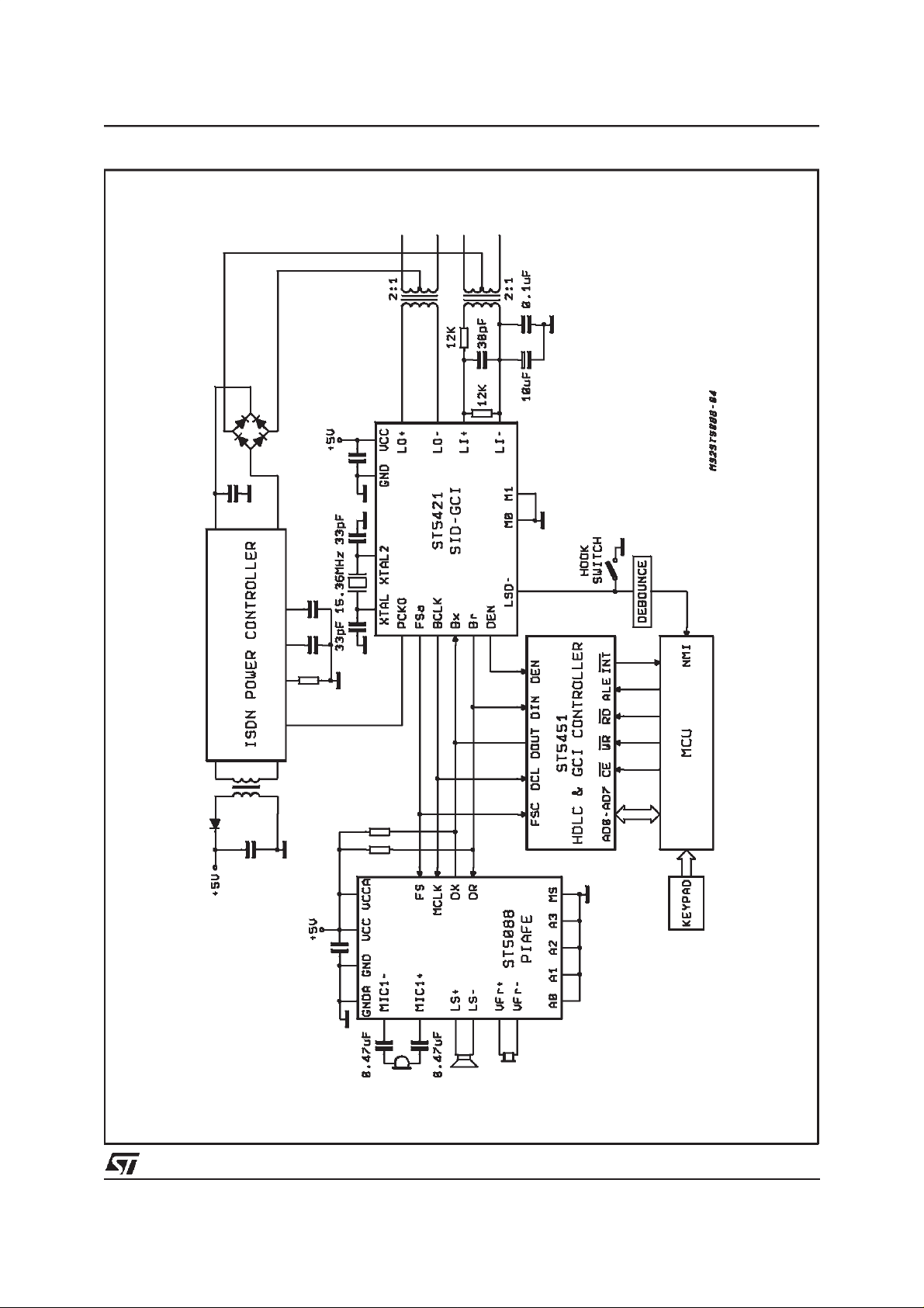
TYPICALISDN TELEPHONE SET APPLICATION
ST5088
3/33
Page 4
ST5088
GENERAL DESCRIPTION
ST5088 PIAFE is a combined PCM CODEC/FILTERdeviceoptimizedfor ISDNTerminalsand Digital Telephone applications. This device is A-law
and Mu-lawselectable and offers a number ofprogrammable functions accessed through a serial
controlchannel.
Depending on mode selected, channel control is
provided by means of a separate serial channel
control MICROWIRE compatible or multiplexed
with the PCM voice data channel in a GCI compatible format requiring only 4 digital interface
pins. When separate serial control interfaceis selected, PCM interface is compatible with Combo I
and Combo II families of devices such as
ETC5057/54,TS5070/71.
PIAFE is built using SGS-THOMSON’s advanced
HCMOS process.
Transmitsection of PIAFE consists of an amplifier
with switchable high impedance inputs followed
by a programmable gain amplifier, an active RC
antialiasingpre-filter to provideattenuationof high
frequency noise, an 8th order switched capacitor
band pass transmit filter and an A-law/Mu-law selectable compandigencoder.
Receive section consist of an A-law/Mu-law selectable expanding decoder which reconstructs
the analog sampled data signal, a 3400 Hz low
pass filter with sin X/X correction followed by two
separate programmable attenuation blocks and
two power amplifiers: one can be used to drive an
earpiece, and the other to drive a 50 Ω loud-
speakeror a piezo transducerup to 600nF.
When the loudspeaker section is set up with
maximum gain (+27dB) the device provide internally a programmable digital anticlipping system
to avoid output distortion.
Programmable functions on PIAFE include a
Ring/Tone generator which provides one or two
tones and can be directed to earpiece or to loudspeaker(or buzzer).
A simple ringer control interface can bypass µP
control of sweep frequency and ring ON/OFF
phases.
A separate programmable gain amplifier allows
gain control of the signal injected. Ring/Tone generator provides sinewave or squarewave signal
with precise frequencies which may be also directed to the input of the Transmit amplifier for
DTMF tone generation.
An auxiliary analog input (EAIN) is also provided
to enable for example the output of an external
band limited Ring signal to the Loudspeaker.
Transmit signal may be fed back into the receive
ampifier with a programmable attenuation to provide a sidetonecircuitry.
A switchable anti-accoustic feed-back system
cancelsthe larsen effect in speech monitoring application.
Two additional pins are provided for insertion of
an external Handfree functionin the Loudspeaker
receivepath.
An output latch controlled by register programming permits external device control.
PIN FUNCTIONS
SO
1,2 1,2 HFI, HFO Hands free I/Os:
3,4 3,4 V
55 V
6,7 6,7 LS-,LS+ Receive analog loudspeaker amplifier complementary outputs,
4/33
PLCC
Name Description
Thesetwopins canbe usedtoinsert an externalHandfreecircuit
suchasthe TEA7540in thereceivepath.HFOisanoutput which
providesthesignalissuedfromoutput ofthe receive low pass filter
whileHFIis a highimpendance input whichis connected directly to
oneof theinputs ofthe Loudspeaker amplifier.
Fr+,VFr–
CC
Receive analog earpiece amplifier complementary
outputs, capable of driving load impedances between 100
and 400 Ω or a piezo ceramic t ransducer up to 150nF.
These outputs can drive directly earpiece transductor. The
signal at this output can drive be the summ of:
- Receive Speech signal from D
- Internal Tone Generator,
- Sidetone signal.
Positive power supply input for the digital section. +5 V + 10%.
intended for driving a Loudspeaker: 80 mW on 50Ω load
impedance can be provided at low distorsion meeting
specifications.
Alternatively this stage can drive a piezo transducer up to
600nF. The signal at these outputs can be the sum of:
- Receive Speech signal from D
- Internal Tone generator,
- External input signal from EAIN input.
,
R
,
R
Page 5

PIN FUNCTIONS (continued)
ST5088
SO
PLCC
Name Description
8 8,9 GND Ground: All digital signals are referenced to this pin.
9 10 MS Mode Select: This input selects COMBO I/II interface mode
with separate MICROWIRE Control interface when tied high
and GCI mode when tied low.
10 11 D
X
Transmit Data ouput: Data is shifted out on this pin during the
assigned transmit time slots. Elsewhere D
output is in the
X
high impendance state. In COMBO I/II mode, voice data byte
is shifted out from TRISTATE output D
at the MCLK
X
frequency on the rising edge of MCLK. In GCI mode, voice
data byte and control bytes are shifted out from OPEN-DRAIN
output D
at half the MCLK. An external pull up resistor is
X
needed.
11 12 AT Alternate Tone: Ring frequency out is controlled without µP
intervention. Tri-state logic controls: f1 (Vcc), f2 (GND), pause
(High Impedance).
14 15 D
R
Receive data input: Data is shifted in during the assigned
Received time slots. In the COMBO I/II mode, voice data byte
is shifted in at the MCLK frequency on the falling edges of
MCLK. In the GCI mode, PCM data byte and contol byte are
shifted in at half the MCLK frequency on the receive rising
edges of MCLK.There is one period delay between transmit
rising edge and receive rising edge of MCLK.
15 16 FS Frame Sync input: This signal is a 8kHz clock which defines
the start of the transmit and receive frames. Either of three
formats may be used for this signal: non delayed timing mode,
delayed timing and GCI compatible timing mode.
16 17 MCLK Master Clock Input: This signal is used by the switched
capacitor filters and the encoder/decoder sequencing logic.
Values must be 512 kHz, 1.536 MHz, 2.048 MHz or 2.56 MHz
selected by means of Control Register CRO. MCLK is used
also to shift-in and out data. In GCI mode, 2.56 MHz and 512
kHz are not allowed.
17 18 LO Open drain output:
a logic 1 written into DO (CR1) appears at LO pin as a logic 0
a logic 0 written into DO puts LO pin in high impedance.
18 – N. C. No connected.
21 22 MIC2+ Alternative positive high impedance input to transmit pre-
amplifier.
22 23 MIC1+ Positive high impedance input to transmit pre-amplifier for
microphone symetrical connection.
23 24 MIC1- Negative high impedance input to transmit pre-amplifier for
microphone symetrical connection.
24 21 TRO Tape Recorder Output: This pin provides the analog
combination of Tx voice signal and Rx voice signal.
25 25 V
CCA
Positive power supply input for the analog section.
+5 V + 10%. V
CC
and V
must be directly connected
CCA
together .
26 26 MIC2- Alternative negative high impedance input to transmit pre-
amplifier.
27 27 GNDA Analog Ground: All analog signals are referenced to this pin.
GND and GNDA must be connected together close to the
device.
28 28 EAIN ExternalAuxiliary input: This input can be used to provide
alternate signals to the Loudspeaker in place of Internal Ring
generator. Input signal should be voice band limited.
5/33
Page 6
ST5088
Following pin definitions are used only when COMBO I/II mode with separate MICROWIRE compatible serial control port is selected. (MS inputset equal one)
PIN FUNCTIONS (continued)
SO
12 13 CO Control data Output: Serial control/status information is shifted
13 14 CI Control data Input:SerialControl information is shiftedintothe
19 19 CCLK Control Clock input: This clock shifts serial control information
20 20 CS- Chip Select input: When this pin is low, control information is
PLCC
Name Description
out from the PIAFE on this pin when CS- is low on the falling
odges of CCLK.
PIAFEon thispin when CS- islow on the rising edges of CCLK.
into CI and out from CO when the CS- input is low, depending
on the current instruction. CCLK may be asynchronous with
the other system clocks.
written into and out from the PIAFE via CI and CO pins.
Followingpin definitions are used only when the GCI mode is selected.(MS input set equal zero)
PIN FUNCTIONS (continued)
SO
19,13,12,20 19,14,13,20 A0,A1,A2,A3 These pins select the address of PIAFE on GCI interface and
PLCC
FUNCTIONAL DESCRIPTION
Power on initialization:
When power is first applied, power on reset
cicuitryinitializes PIAFE and puts it into the power
Name Description
must be hardwired to either V
C4,C5,C6,C7 bits of the first address byte respectively.
or GND. A0,A1,A2,A3 refer to
CC
When a power up command is given, all de-activated circuits are activated, but output D
main in the high impedance state on B time slots
until the second Fs pulse after power up, even if a
B channel is selected.
will re-
X
down state. Gain Control Registersfor the various
programmable gain amplifiers and programmable
switches are initialized as indicated in the Control
Register description section. All CODEC functions
are disabled.Digital Interface is configuredin GCI
mode or in COMBOI/II mode dependingon Mode
Select pin connection.
The desired selection for all programmable functions may be intialized prior to a power up command using Monitor channel in GCI mode or MICROWIREport in COMBOI/II mode.
Power down state:
Following a period of activity, power down state
may be reentered by writing a power down instruction.
ControlRegisters remain in their current state and
can be changedeither by MICROWIREcontrol interface or GCI control channel depending on
modeselected.
In addition to the power down instruction, detection of loss MCLK (no transition detected) automatically enters the device in ”reset” power down
Power up/down control:
Following power-on initialization, power up and
state with D
output in the high impedance state
X
and L0 in high impedancestate.
power down control may be accomplishedby writing any of the control instructions listed in Table 1
into PIAFE with ”P” bit set to 0 for power up or 1
for power down.
Normally, it is recommended that all programmable functions be initially programmed while the
device is powered down. Power state control can
then be included with the last programming instruction or in a separatesingle byte instruction.
Any of the programmable registers may also be
modified while ST5088 is powered up ordown by
setting ”P” bit as indicated. When power up or
down control is entered as a single byte instruction, bit 1 must be set to a 0.
Transmitsection:
Transmit analog interface is designed in two
stages to enable gains up to 35 dB to be realized.
Stage 1 is a low noise differential amplifierprovid-
ing 20 dB gain. A microphone may be ca-
pacitevely connected to MIC1+, MIC1- inputs,
while the MIC2+ MIC2– inputs may be used to
capacitively connect a second microphone (for
digital handsfree operation) or an auxiliary audio
circuitsuch as TEA 7540 Hands-free circuit. MIC1
or MIC2 source is selected with bit 7 of register
CR4.
Following the first stage is a programmable gain
6/33
Page 7

ST5088
amplifier which provides from 0 to 15 dB of additional gain in 1 dB step. The total transmit gain
should be adjusted so that, at reference point A,
see Block Diagram description, the internal 0
dBmO voltage is 0.739 V (overload level is 1.06
Vrms). Second stage amplifier can be programmed with bits 4 to 7 of CR5. To temporarily
mute the transmit input, bit TE (6 of CR4) may be
set low. In this case, the analog transmit signal is
grounded and the sidetonepath is also disabled.
An activeRC prefilterthenprecedes the 8th order
band pass switched capacitor filter. A/D converter
has a compressing characteristic according to
CCITT A or mu255 coding laws, which must be
selected by setting bits MA, IA in register CR0. A
precision on chip voltage reference ensuresaccurate and highly stabletransmission levels.
Any offset voltage arising in the gain-set amplifier,
the filtersor the comparatoris cancelled by an internalautozero circuit.
Each encode cycle begins immediatly at the beginning of theselected Transmit time slot. The total signal delay referenced to the start of thetime
slot is approximatively195 µs (due to the transmit
filter) plus 123 µs (due to encoding delay), which
totals 320 µs. Voice data is shifted out on D
X
during the selected time slot on the transmit rising
adges of MCLK.
Receive section:
Voice Data is shifted into the decoder’s Receive
voice data Register via the D
pin during the se-
R
lected time slot on the 8 receiveedges of MCLK.
The decoder consists of an expandingDAC with
either A or MU255 law decoding characteristic
which is selected by the same control instruction
used to select the Encode law during intitialization. Following the Decoder is a 3400 Hz 6th order low pass switched capacitorfilter with integral
Sin X/X correctionfor the 8 kHz sample and hold.
0 dBmO voltage at this (B) reference point (see
Block Diagram description) is 0.49 Vrms. A transcient suppressing circuitry ensure interference
noise suppressionat power up.
The analog speech signal output can be routed
either to earpiece (V
FR+,VFR-
outputs) or to loudspeaker (LS+, LS- outputs) by setting bits SL and
SE (1and 0 of CR4).
Total signal delay is approximatively190 µs (filter
plus decoding delay) plus 62.5 µs (1/2 frame)
which gives approximatively252 µs.
Differential outputs V
FR+,VFR-
are intended to directly drive an earpiece. Preceding the outputs is
a programmableattenuationamplifier, which must
be set by writing to bits 4 to 7 in register CR6. Attenuationsin the range 0 to -15 dB relativeto the
maximum level in 1 dB step can be programmed.
The input of this programmable amplifier is the
summ of several signals which can be selected
by writing to register CR4.:
- Receive speech signal which has been decodedand filtered,
- Internally generated tone signal, (Tone amplitude is programmed with bits 4 to 7 of register
CR7),
- Sidetone signal, the amplitude of which is programmedwith bits 0 to 3 of registerCR5
V
FR+
andV
outputsarecapableof drivingoutput
FR-
power level up to 14mW into differentially connectedloadimpedancebetween100 and 400Ω.
Differential outputs LS+,LS- are intended to directly drive a Loudspeaker.Preceding the outputs
is a programmable attenuation amplifier, which
must be set by writing to bits 0 to 3 in register
CR6. Attenuations in the range 0 to -30 dB relative to the maximum level in 2.0 dB step can be
programmed.The input of this programmableamplifier can be the summ of signals which can be
selectedby writing to register CR4:
- Receive speech signal which has been decodedand filtered,
- Internally generated tone signal, (Tone amplitude is programmed with bits 4 to 7 of register
CR7),
- EAIN input which may be an alternate Ring
signal or any voice frequency band limited
signal. (An external decoupling capacitor of
about0.1µF is necessary).
Receive voice signal may be directed to output
HFO by means of bit HFE in Register CR4. After
processing, signal must be re-enteredthrough input HFI to Loudspeakeramplifier input. (An external decoupling capacitor of about 0.1µF is necessary).
The output loudspeaker section has two switchable gains of +9dB and +27dB.
+9dB LS Gain
This gain mode is fully equivalent to PIAFE
ST5080 behaviour.
LS+ and LS- outputs are capableof driving output
power level up to 80 mW into 50Ωdifferentially
connectedload impedance at low distortion meeting PCM channel specifications. When the signal
source is a Ring squarewavesignal, power levels
up to approximatively200 mW can be delivered.
+27dBLS Gain
Additional gain of 18dB has the purpose to increase the undistorted output power up to
150mW typical with digital input DR ranging from
-12dBm0to +3dBm0.
Output DC offset is limited by high pass filter with
35Hz cut frequency (wit h LS gain = +9dB cut frequency = 9Hz)
Anti-acoustic feed-back for loudspeakerto handset microphone loop with squelch effect: on chip
7/33
Page 8

ST5088
switchable anti-larsen for loudspeaker to handset
microphone feedback is implemented. A 12dB
depth gain control on both transmit and receive
path is provided to keep constant the loop gain.
On the transmit path the 12dB gain control is provided starting from the CR5 transmit gain definition; at the same time, on the receive path the
12dB gain control is provided starting from CR6
receive gain definition.
DIGITAL ANTICLIPPINGSYSTEM(D.A.S.)
An automatic anticlipping system is necessary to
avoid distortion on LS+/LS- when the output
swing approaches the supply rails. (LS GAIN >>
+9dB).
The digital anticlipping system calculates equivalent input signal on DR pin and compares it with a
selectable anticlipping threshold. The D.A.S. is
then able to reduce the overall gain in order to
avoid or limit the distortion.
Four different thresholds are programmable via
register:
-15dBm0 D < 1% For safe margin
-13dBm0 D = 1% For normal operation
-9dBm0 D ≥ 1% Fornoisy ambient (*)
-7dBm0 D >> 1% For very noisy ambient (*)
(*) When environment is noisy, power output
might be more important than 1% distortion.
Gain reduction of the D.A.S. (Anticlipping Attack)
has a fixedspeed of 8KHz.
Gain recovery or increase (Anticlipping Release)
has 4 programmable speeds of 4Hz, 8Hz, 31Hz
and 62Hz.
TAPE RECORDEROUTPUT(TRO)
This section provides a combinationof Txand Rx
Analog Signals to an external user like a recordering machine. The output levels relative to a
signal of 0dBm0 on channel Dx and DR are:
Rx TRO= 0.245V
Tx TRO = 0.246V
(for0dBm0 on DR)
RMS
(for0dBm0 on DX)
RMS
The single ended Op Amp is able to drive an externalload as low as 600Ω.
ALTERNATE TONE CONTROL(AT)
This section allows to simplifythe microprocessor
control of ringeroperation. When pin AT is put externally at high impedance state (or left open) the
control of ring frequency emission is totally
through a microprocessor, which updates in real
time the contents of various registers.
When pin AT is forced at GND or Vcc the ring
generator emits respectively the frequencies f2
(GND) and f1 (Vcc), previously defined through
registers CR9 (f2) and CR8(f1). This operative
mode requires only start-up interventionof the mi-
croprocessor.
Digitaland Control Interface:
PIAFE provides a choice of either of two types of
Digital Interface for both control data and PCM.
For compatibilitywith systems which use time slot
oriented PCM busses with a separate Control Interface, as used on COMBO I/II families of devices, PIAFE functions are describedin next section.
Alternatively, for systems in which PCM and control data are multiplexedtogether using GCI interface scheme, PIAFE functions are described in
the section following the next one.
PIAFE will automatically switch to one of these
two types of interfaceby sensingthe MS pin.
Due to Line Transceiver clock recovery circuitry,a
low jitter may be provided on F
clocks. F
and MCLK must be always in phase.
S
and MCLK
S
For ST5421S Transceiver, as an example,
maximun value of jitter amplitude is a step of 65
ns at each GCI frame (125µs). So, the maximum
jitter amplitude is 130 ns pk-pk.
COMBOI/II mode.
DigitalInterface (Fig. 1)
F
Frame Sync input determines the beginningof
S
frame. It may have any duration from a single cycle of MCLK to a squarewave.Two different relationships may be establishedbetween the Frame
Sync input and the first time slot of frame by setting bit 3 in register CR0. Non delayed data mode
is similar to long frame timing on ETC5057/
TS5070 series of devices (COMBO I and
COMBO II respectively): first time slot begins
nominally coincident with the rising edge of F
S
Alternative is to use delayed data mode, which is
similar to short frame sync timing on COMBO I or
COMBO II, in which F
inputmust be high at least
S
a half cycle of MCLK earlier the frame beginning.
A time slot assignment circuit on chip may be
used with both timing modes, allowing connection
to one of the two B1 and B2 voice data channels.
Two data formats are available: in Format 1, time
slot B1 corresponds to the 8 MCLK cycles following immediately the rising edge of FS, while time
slot B2 corresponds to the 8 MCLK cycles following immediately time slot B1.
In Format 2, time slot B1 is identical to Format 1.
Time slot B2 appears two bit slots after time slot
B1. This two bits space is left available for insertion of the D channel data.
Data format is selected by bit FF (2) in register
CR0. Time slot B1 or B2 is selected by bit T0 (0)
in Control Register CR1.
Bit EN (2) in control register CR1 enables or disables the voice data transfer on D
and DRas
X
appropriate. During the assigned time slot, D
.
X
8/33
Page 9
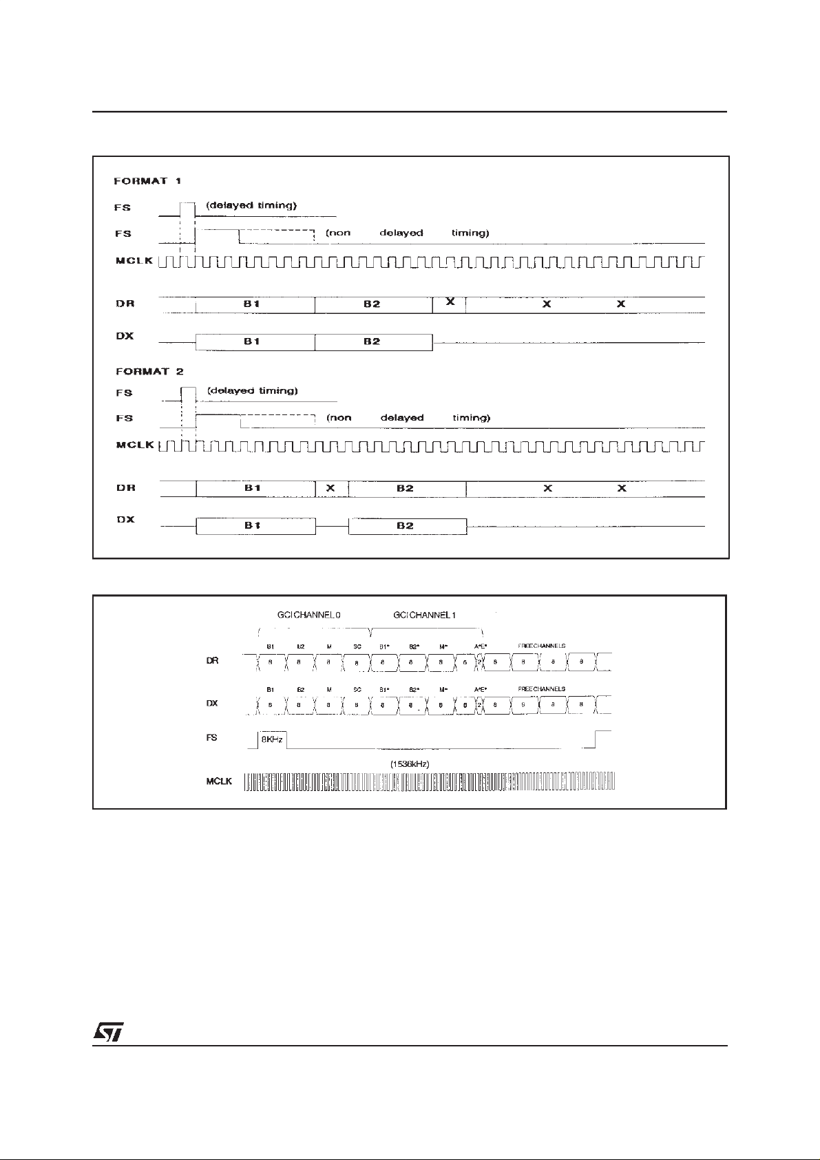
Figure 1: Digital Interface Format
ST5088
Figure 2: GCI InterfaceFrame Structure
output shifts data out from the voice data register
on the rising edges of MCLK. Serial voice data is
shifted into D
input during the same time slot on
R
the falling edges of MCLK.
D
is in the high impedance Tristate condition
X
when in the non selectedtime slots.
ControlInterface:
Control informationor data is written into or readback from PIAFE via the serial control port consisting of control clock CCLK, serial data input CI
and output CO, and Chip Select input, CS-. All
control instructionsrequire 2 bytes as listed in Ta-
ble 1, with the exception of a single byte powerup/down command.
To shift control data into ST5088, CCLK must be
pulsed high 8 times while CS- is low. Data on CI
input is shifted into the serial input registeron the
rising edge of each CCLK pulse. After all data is
shifted in, the content of the input shift register is
decoded, and may indicate that a 2nd byte of
control data will follow. This second byte may
either be defined by a second byte-wide CSpulse or may follow the first contiguously, i.e. it is
not mandatory for CS- to return high in between
the first and second control bytes. At the end of
9/33
Page 10

ST5088
the 2nd control byte, data is loaded into the appropriate programmable register. CS- must return
high at the endof the 2nd byte.
To read-back status information from PIAFE, the
first byte of the appropriate instruction is strobed
in during the first CS- pulse, as defined in Table
1. CS- must be set low for a further 8 CCLK cycles, during which data is shifted out of the CO
pin onthe falling edges of CCLK.
When CS- is high, CO pin is in the high impedance Tri-state, enabling CO pins of several devices to be multiplexedtogether.
Thus, to summarise,2 byte READ and WRITE instructions may use either two 8-bit wide CSpulses or a single16 bit wide CS-pulse.
Controlchannel access to PCM interface:
It is possible to access the B channel previously
selected in Register CR1.
A byte written into Control Register CR3 will be
automatically transmitted from D
output in the
X
followingframe in place of the transmit PCM data.
A byte written into Control Register CR2 will be
automatically sent through the receive path to the
Receiveamplifiers.
In order to implement a continuousdata flow from
the Control MICROWIRE interface to a B channel, it is necessary to send the control byte on
each PCM frame.
A current byte received on D
input can be read
R
in the register CR2. In order to implement a continuous data flow from a B channel to MICROWIREinterface, it is necessary to read register CR2 at each PCM frame.
GCI COMPATIBLEMODE
GCI interface is an European standardized interface to connect ISDN dedicated components in
the different configurations of equipment as Terminals, NetworkTerminations,PBX, etc...
In a Terminal equipment, this interface called
SCIT for SpecialCircuit Interface for Terminals allows for exampleconnection between:
- ST5421 (SID-GCI) and ST5451 (HDLC/GCI
controller)used for 16 kbit/s D channel packet
framesprocessingand SID control,
- Peripheraldevices connected to a 64 kbit/s B
channel and ST5451 used for GCI peripheral
control.
ST5088 may be assigned to one of the B channels present on the GCI interface and is monitored via a control channel which is multiplexed
with the 64 kbit/sVoice Data channels.
Figure 2 shows the frame structure at the GCI interface. Two 256 kbit/s channel are supported.
a)GCI channel 0: It is structured in four sub-
channels:
–B1 channel 8 bits per frame
–B2 channel 8 bits per frame
–M channel8 bitsperfra m eignoredbyPIAFE
–SC channel 8 bits per frame ignored by
PIAFE
Only B1 or B2 channelcan be selected in
PIAFEfor PCM data transfer.
b)GCI channel 1: It is structured also in four
subchannels:
–B1* channel 8 bits per frame
–B2* channel 8 bits per frame
–M* channel 8 bitsper frame
–SC* which is structuredas follows:
6 bits ignored by PIAFE
A* bit associatedwith M* channel
E* bit associatedwith M* channel.
B1*or B2* channel can be selectedin PIAFE
for PCM data transfer.
M*channel and twoassociated bitsE* and A*
areused for PIAFEcontrol.
Thus, to summarize, B1, B2, B1* or B2* channel
can be selected to transmit PCM data and M*
channel is used toread/write status/commandperipheral device registers. Protocol for byte exchange on the M* channel usesE* and A* bits.
Physical Interface
The interfaceis physically constitued with 4 wires:
InputData wire: D
OutputData wire: D
R
X
Bit Clock: MCLK
Frame Synchronization: F
S
Data is synchronized by MCLK and FSclock inputs.
F
insures reinitialization of time slot counter at
S
each frame beginning. The rising edge or FS is
the referencetime for the first GCI channel bit.
Data is transmitted in both directions at half the
MCLK input frequency. Data is transmitted on the
the rising edge of MCLK and is sampled one period after the transmit rising edge, also on a rising
edge.
Note: Transmit data may be sampled by far-end
device ie SID ST5421 on the falling edge 1.5 period afterthetransmit rising edge.
Unused channel are high impedance. Data outputs are OPEN-DRAIN and need an external pull
up resistor.
COMBOactivation/deactivation
ST5088 is automatically set in power down mode
when GCI clocks are idle. GCI section is reactivated when GCI clocks are detected. PIAFE is
completly reactivated after receiving of a power
up command.
Exchangeprotocol on M* channel
10/33
Page 11

ST5088
Protocol allows a bidirectional transfer of bytes
between ST5088 and GCIcontroller with acknowledgment at each received byte. For PIAFE,
standard protocol is simplified to provide read or
write register cycles almost identical to MICROWIREserial interface.
Write cycle
Control Unit sends through the GCI controller following bytes:
- First byte is the chip select byte. The first four
bits indicate the device address:
(A3,A2,A1,A0).The four last bits are ignored.
ST5088 compare the validated byte received
internallywith the addressdefined by pins A3,
A2, A1, A0. If comparison is true, byte is acknowledged,if not, ST5088 does not acknowledgethe byte.
NOTE: An internal ”message in progress” flag remains active till the end of the completemessage
transmissionto avoid irrelevant acknowledgement
of any furtherbyte.
- Second byte is structured as defined in Table 1.
- Third byte is the Data byte to write into the
Registeras indicated in Table 1.
It is possiblebut optional to write to several different registersin a single message. In this case the
Chip Select byte is sent only once at the beginning of the message, the device automatically
togglesbetween address byte and data byte.
Read cycle
Control Unit sends two bytes. First byte is the
chip select byte as defined above. Second byte is
structuredas defined in Table 1.
If PIAFE identifies a read-back cycle, bit 2 of byte
1 in Table 1 equal 1, it has to respond to the Control Unit by sending a single byte message which
is the content of the addressed register.
It is possible but optional to request several different read-backregister cycles in a singlemessage
but it is recommended to wait the answer before
requesting a new read back to avoid loss of data.
ST5088 responds by sending a single data byte
message at each request.
Received byte validation:
A received byte is validated if it is detected two
consecutivetimes identical.
ExchangeProtocol:
Exchangeprotocol is identical for both directions.
Sender uses E* bit to indicate that it is sending a
M* byte while receiver uses A* bit to acknowledge
received byte.
When no message is transferred, E* bit and A* bit
are forcedto inactive state.
A transmission is initialized by sender putting E*
bit from inactive state to active state and by sending first byte on M* channel in the same frame.
Transmission of a message is allowed only if A*
bit from the receiver has been set inactive for at
leasttwo frames.
When receiver is ready, it validates the received
byte internally when received in two consecutive
frames identical. Then the receiver sets first A* bit
from inactive to active state (pre-acknowlegement), and maintains A* bit active at least in
the following frame (acknowledgement).If validation is not possible, (two last bytes received are
not identical), receiver aborts the message setting
A* bit active for only a single frame.
For the first byte received, Abort sequence is not
allowed. PIAFE does not respond either if two last
bytes are not identical or if the byte received does
not meet the Chip Select byte defined by A0-A3
pins bias.
A second byte may be transmitted by the sender
putting E* bit from active to inactive state and
sending the second byte on the M* channel in the
same frame. E* bit is set inactive for only one
frame. If it remains inactive more than one frame,
it is an end of message (i.e. not second byte
available).
The secondbyte may be transmitted only after receiving the pre-acknowledgment of the previous
byte transmitted (see Fig. 3). The same protocol
is used if a third byte is transmitted. Each byte
has to be transmitted at least in two consecutive
frames.
The receiver validates current received byte as
done on first byte and then set A* bit in the next
two frames first from active to inactive state (preacknowledgement),and after from inactive to active state (acknowledgement).If the receiver cannot validate the received current byte (two bytes
received are not identical), it pre-acknowledges
normally, but let A* bit in the inactive state in the
next frame which indicates an abort request.
If a message sent by ST5088 is aborted, it will
stop the message and wait for a new read cycle
instructionfromthe controller.
A message received by ST5088 is acknowledged
or aborted without flow Control.
Figures 3 gives timing of a write cycle. Most significant bit (MSB) of a Monitorbyte is sent first on
M* channel.
E* and A* bits are active low and inactive state on
DOUTis high impedance.
PROGRAMMABLE FUNCTIONS
11/33
Page 12

ST5088
Figure 3: E and Abits Timing
12/33
Page 13

ST5088
For both formats of Digital Interface, programmable functions are configured by writing to a number of registersusing a 2-byte write cycle (not including chip select byte in GCI).
verification. Byte one is always register address,
while byte two is Data.
Table 1 lists the register set and their respective
adresses.
Most of these registers can also be read-back for
Table 1: ProgrammableRegister Intructions
Function Address byte
76543210
Single byte Power up/down P X X X X X 0 X none
Write CR0 P 0 00001XseeCR0TABLE 2
Read-back CR0 P 0 00011XseeCR0
Write CR1 P 0 00101XseeCR1TABLE 3
Read-back CR1 P 0 00111XseeCR1
Write Data to receive path P 0 01001XseeCR2TABLE 4
Read data from D
Write Data to D
Write CR4 P 0 10001XseeCR4TABLE 6
Read-back CR4 P 0 10011XseeCR4
Write CR5 P 0 10101XseeCR5TABLE 7
Read-back CR5 P 0 10111XseeCR5
Write CR6 P 0 11001XseeCR6TABLE 8
Read-back CR6 P 0 11011XseeCR6
Write CR7 P 0 11101XseeCR7TABLE 9
Read-back CR7 P 0 11111XseeCR7
Write CR8 P 1 00001XseeCR8TABLE 10
Read-back CR8 P 1 00011XseeCR8
Write CR9 P 1 00101XseeCR9TABLE 11
Read-back CR9 P 1 00111XseeCR9
Write CR10 P 1 01001XseeCR10 TABLE 12
Read-back CR10 P 1 01011XseeCR10
R
X
P001011XseeCR2
P001101XseeCR3TABLE 5
Data byte
NOTE 1: bit7 of the address byte and data byte is always the first bit clocked into or out from: CI and CO pins when MICROWIRE serial
port is enabled, or into and out from D
X = reserved: write 0
NOTE 2: ”P” bit is Power up/downControl bit. P = 1 Means Power Down.
Bit 1 indicates, if set, the presence of a second byte.
NOTE 3: Bit 2 is write/read select bit.
and DXpins when GCI mode selected.
R
13/33
Page 14

ST5088
Table 2: Control Register CR0 Functions
76543210
F1 F0 MA IA DN FF B7 DL
0
0
1
0
0
1
1
1
0
0
1
0
0
1
1
1
0
1
0
1
0
1
*: state at power on initialization
(1): significant in COMBO I/II mode only
MCLK = 512 kHz
MCLK = 1.536 MHz
MCLK = 2.048 MHz
MCLK = 2.560 MHz
MU-law; CCITT D3-D4
MU-law; Bare Coding
A-law including even bit inversion
A-law; Bare Coding
Delayed data timing
Non delayed data timing
B1 and B2 consecutive
B1 and B2 separated
8 bits time-slot
7 bits time-slot
01Normal operation
Digital Loop-back
Function
(1)
*
(1)
*
*(1)
(1)
*(1)
(1)
*
*
Table 3: Control Register CR1 Functions
76543210
HFE ALE DO MR MX EN T1 T0
0
1
0
1
0
1
0
1
0
1
0
1
0
0
1
1
*: state at power on initialization
(1): significant in COMBO I / II mode only
(2): significant in GCI mode only.
HFO / HFI pins disabled
HFO / HFi pins enabled
Anti-larsen disabled
Anti-larsen enabled
L0 latch is put in highimpedance
L0 latch set to 0
D
connected to rec. path
R
CR2 connected to rec. path
Trans path connected to D
CR3 connected to D
X
voice data transfer disable
voice data transfer enable
B1 channel selected
0
B2 channel selected
1
B1* channel selected
0
B2* channel selected
1
Function
X
*
*
*
* (1)
(1)
* (1)
(1)
*
*
(2)
(2)
14/33
Page 15

Table 4: ControlRegister CR2 Functions
ST5088
76543210
d7 d6 d5 d4 d3 d2 d1 d0
msb lsb Data sent to Receive path or Data received from D
Function
Table 5: Control Registers CR3 Functions
76543210
d7 d6 d5 d4 d3 d2 d1 d0
msb lsb D
data transmitted
X
Function
Table 6: Control Register CR4 Functions
76543210
VS TE SI EE RTL RTE SL SE
0
1
0
1
0
1
0
1
0
0
1
0
0
1
1
1
0
0
1
0
0
1
1
1
MIC1 selected
MIC2 selected
Transmit input muted
Transmit input enabled
Internal sidetone disabled
Internal sidetone enabled
EAIN disconnected
EAIN selected to Loudspeaker
Ring / Tone muted
Ring / Tone to Earpiece
Ring / Tone to Loudspeaker
Ring / Tone to Earpiece and Loudspeaker
Receive signal muted
Receive signal connected toearpiece amplifer
Receive signal connected toloudspeaker amplifier
Receive signal connected toloudspeaker and
earpiece amplifier
Function
R
input
*
*
*
*
*
*
*: state at power on initialization
15/33
Page 16

ST5088
Table 7: Control Register CR5 Functions
76543210
Transmit amplifier Sidetone amplifier
0
0
0
-
1
1
*: state at power on initialization
1
0
-
1
1
0
0
0
0
-
1
0
0
-
1
1
0
0
0
Table 8: Control Register CR6 Functions
76543210
Earpiece ampifier Loudspeaker
0
0
0
0
0
0
-
1
1
*: state at power on initialization
1
0
-
1
1
0
0
0
0
-
1
0
0
-
1
1
0 dB gain
1 dB gain
in 1 dB step
15 dB gain
-8 dB gain
0
-9 dB gain
1
in 1 dB step
-
-23 dB gain
1
0 dB gain
-1 dB gain
in 1 dB step
-15 dB gain
0 dB gain
0
-2 dB gain
1
in 2 dB step
-
-30 dB gain
1
Function
*
*
Function
*
*
Table 9: Control Register CR7 Functions
7 6 5 4 3 2 1 0 Function
Tone gain F1 F2 SN DE Attenuation f1 V
0
0
0
0
0
0
0
1
0
1
0
1
0
1
0
X
1
X
1
1
0
0
1
1
1
0
0
1
0
0
1
1
1
0
X
1
X
0
0
1
0
0
1
1
1
0
0
0
0
1
*: state at power on initialization
(1): value provided if f1 or f2 is selected alone.
X reserved: write 0
if f1 and f2are selected in the summedmode, f1=1.34V
Outputgenerator is 2.4 V
pp
....0dB*
-3dB
-6dB
-9dB
-12 dB
-15 dB
-18 dB
-21 dB
-24 dB
-27 dB
f1 and f2 muted
f2 selected
f1 selected
f1 and f2 in summed mode
Squarewave signal selected
Sinewave signal selected
01Normal operation *
Tone / Ring Generator connected toTransmit path
whilef2=1.06 Vpp.
pp
...2.4 (1)
1.70
1.20
0.85
0.60
0.43
0.30
0.21
0.15
0.10
pp
f2 V
pp
....1.9 (1)
1.34
0.95
0.67
0.47
0.34
0.24
0.17
0.12
0.08
*
*
16/33
Page 17

Table 10: Control Register CR8 Functions
ST5088
76543210
f17 f16 f15 f14 f13 f12 f11 f10
msb lsb Binary equivalent of the decimal number used to calculate f1
Function
Table 11: Control Register CR9 Functions
76543210
f27 f26 f25 f24 f23 f22 f21 f20
msb lsb Binary equivalent of the decimal number used to calculate f2
Function
Table 12: Control Register CR10 Functions
76543210
GLS ACE VT1 VT0 FD1 FD0 DFT HFT
1
0
1
0
0
0
1
0
0
1
1
1
0
0
1
0
0
1
1
1
0
0
1
1
(*) Default values inserted into the Register atPower On.
+27 dB into LH Path
(*) +9dB intoLH Path
Anticlipping ON
(*) Anticlipping OFF
(*) -15dm0 Anticlipping Threshold
-13dm0 Anticlipping Threshold
-9dm0 Anticlipping Threshold
-7dm0 Anticlipping Threshold
(*) 256ms Gain Recovery Time Constant / (4Hz)
128ms Gain recovery Time Constant / (8Hz)
32ms Gain Recovery TimeConstant / (31Hz)
16ms Gain Recovery TimeConstant / (62Hz)
(*) Standard Frequency ToneRange
0
Halved Frequency Tone Range
1
Doubled Frequency Tone Range
0
Forbidden
1
Function
17/33
Page 18

ST5088
CONTROLREGISTERCR0
First byte of a READ or a WRITE instruction to
Control Register CR0 is as shown in TABLE 1.
Secondbyte is as shown in TABLE 2.
2.048MHz.
512KHzand 2.56MHz are not allowed.
Defaultvalue is 1.536 MHz for both modes.
Any clock different from the default one must be
selected prior a Power-Up instruction for both
MasterClock Frequency Selection
modes.
A master clock must be provided to PIAFE for operation of filter and coding/decodingfunctions.
In COMBO I/II mode, MCLK frequency can be
either 512 kHz, 1.536 MHz, 2.048 MHz or 2.56
MHz.
Bit F1 (7) and F0 (6) mustbe set during initialization to selectthe correct internal divider.
Coding Law Selection
Bits MA (5) and IA (4) permit selection of Mu-255
law or A law coding with or without even bit inver-
sion.
After power on initialization, the Mu-255 law is se-
lected.
In GCI mode, MCLK must be either 1.536MHzor
Mu 255 law
msb lsb msb lsb msb lsb
Vin = + full scale 1 0 0000001010101011111111
Vin = 0 V
Vin = - full scale 0 0 0000000010101001111111
MSB is always the first PCMbit shifted in or out of PIAFE.
10111111111111111011001100110011100000000000000
True A law even bit
inversion
A law without even bit
inversion
0
Digital Interfacetiming
Bit DN=0 (3) selects digital interface in delayed
timing mode while DN=1 selects non delayed
data timing.
In GCI mode, bit DN is not significant.
After reset and if COMBO I/II mode is selected,
delayed data timing is selected.
Digital Interfaceformat
Bit FF=0 (2) selects digital interface in Format 1
where B1 and B2 channel are consecutive. FF=1
selects Format 2 where B1 and B2 channel are
separatedby two bits. (see digital interface format
section).
In GCI mode, bit FF is not significant.
56+8 selection
Bit ’B7’ (1) selects capability for PIAFE to take
into account only the seven most significant bits
of the PCM data byte selected.
When ’B7’ is set, the LSB bit on D
LSB bit on D
is high impedance. This functional-
X
is ignoredand
R
lows connection of an external ”in band” data
generator directly connected on the Digital Interface.
Digital loopback
Digital loopback mode is entered by setting DL
bit(0) equal1.
In Digital Loopback mode, data written into Receive PCM Data Register from the selected received time-slot is read-backfrom that Register in
the selected transmit time-slot on D
. Time slot is
X
selectedwith Register CR1.
No PCM decoding or encoding takes place in this
mode. Transmit and Receive amplifier stages are
muted.
CONTROLREGISTER CR1
First byte of a READ or a WRITE instruction to
Control Register CR1 is as shown in TABLE 1.
Secondbyte is as shown in TABLE 3.
Hands-free I/Os selection
Bit HFE set to one enables HFI, HFO pins for
connectionof an external handfreecircuit such as
TEA 7540. HFO is an analog output that provides
the receive voice signal. 0 dBMO level on that
output is 0.491 Vrms (1.4V
). HFI is an analog
pp
high impedance input (10 KΩ typ.) intended to
send back the processed receive signal to the
Loudspeaker. 0 dBMO level on that input is
0.491Vrms.
Anti-larsenselection
Bit ALE set toone enables on-chip antilarsen and
squelch effect system.
Latchoutput control
Bit DO controls directly logical status of latchout-
put LO: ie, a ”ZERO”written in bit DOputs output
LO in high impedance, a ”ONE” written in bit DO
setsoutput LO to zero.
18/33
Page 19

ST5088
Microwire access to B channel on receive
path
Bit MR (4) selects access from MICROWIRE
Register CR2 to Receive path. When bit MR is
set high, data written to register CR2 is decoded
each frame, sent to the receive path and data input at D
is ignored.
R
In the other direction, current PCM data input received at D
can be read from register CR2 each
R
frame.
Microwire access to B channel on transmit
path
Bit MX (3) selects access from MICROWIREwrite
only Register CR3 to D
set high,data written to CR3 is output at D
output. When bit MX is
X
X
every
frame and the output of PCM encoder is ignored.
B channelselection
Bit ’EN’ (2) enables or disables voice data transferon D
and DRpins.When disabled,PCM data
X
from DR is not decoded and PCM time-slots are
high impedance on D
.
X
In GCI mode, bits ’T1’ (1) and ’T0’ (0) select one
of the four channelsof the GCI interface.
In COMBO I/II mode, only B1 or B2 channel can
be selected according to the interface format selected. Bit ’T1’ is ignored.
CONTROLREGISTERCR2
Data sent to receive path or data received from
D
input. Refer to bit MR(4) in ”Control Register
R
CR1” paragraph.
CONTROLREGISTERCR3
data transmitted. Refer to bit MX(3)in ”Control
D
X
Rgister CR1” paragraph.
CONTROLREGISTERCR4
First byte of a READ or a WRITE instruction to
Control Register CR4 is as shown in TABLE 1.
Secondbyte is as shown in TABLE 6.
TransmitInput Selection
MIC1 or MIC2 source is selectedwith bit VS (7).
Transmit input selected can be enabled or muted
with bit TE (6).
Transmit gain can be adjusted within a 15 dB
range in 1 dB step with RegisterCR5.
loudspeakeramplifier input.
Ring/Tonesignal routing
Bits ”RTL” (3) and RTE (2) provide select capabil-
ity to connect on-chip Ring/Tone generator either
to loudspeakeramplifier input or to earpiece am-
plifier input or both.
PCM receivedata routing
Bits ”SL” (1) and ”SE” (0) provide select capability
to connect received speech signal either to Loud-
speaker amplifier input or to earpieceamplifier in-
put or both.
CONTROLREGISTER CR5
First byte of a READ or a WRITE instuction to
Control Register CR5 is as shown in TABLE 1.
Secondbyte is as shown in TABLE 7.
Transmitgain selection
Transmit amplifier can be programmed for a gain
from 0dB to 15dB in 1dB step with bits 4 to 7.
0 dBmO level at the output of the transmit ampli-
fier (A reference point) is 0.739 Vrms (overload
voltageis 1.06 Vrms).
Sidetoneattenuationselection
Transmit signal picked up after the switched ca-
pacitor low pass filter may be fed back into the
ReceiveEarpiece amplifier.
Attenuation of the signal at the output of the
side tone attenuator can be programmed from
–8dB to –23dB relative to reference point A in
1 dB step with bits 0 to 3.
CONTROLREGISTER CR6
First byte of a READ or a WRITE instruction to
Control Register CR6 is as shown in TABLE 1.
Secondbyte is as shown in TABLE 8.
Earpieceamplifiergain selection:
Earpiece Receive gain can be programmed in 1
dB step from 0 dB to -15 dB relative to the maxi-
mum with bits 4 to 7.
0 dBmO voltage at the output of the amplifier on
pins V
Fr+
and V
is then 824.5 mVrms when
Fr-
0dB gain is selected down to 146.6 mVrms
when –15dB gain is selected.
Sidetoneselect
Bit ”SI” (5) enables or disables Sidetone circuitry.
When enabled, sidetone gain can be adjusted
with Register (CR5). When Transmit path is disabled, bit TE set low, sidetone circuit is also disabled.
ExternalAuxiliary signal select
Bit ”EE” (4) set to one connectsEAIN input to the
Loudspeakeramplifier gain selection:
Loudspeaker Receive amplifier gain can be pro-
grammed in 2 dB step from 0 dB to -30 dB rela-
tive to the maximumwith bits 0 to 3.
0 dBmO voltage on the output of the amplifier on
pins LS+ and LS- on 50 Ω is then 1.384 Vrms
(3.91V
43.7 mVrms (123.6mV
) when 0 dB gain is selected down to
pp
) when -30 dB gain is se-
pp
lected.
19/33
Page 20

ST5088
Current limitation is approximatively150 mApk.
CONTROLREGISTERCR7:
First byte of a READ or a WRITE instruction to
Control Register CR7 is as shown in TABLE 1.
Secondbyte is as shown in TABLE 9.
Tone/Ring amplifier gain selection
Output level of Ring/Tone generator, before attenuation by programmableattenuator is 2.4 Vpkpk when f1 generator is selected alone or
summed with the f2 generator and 1.9 Vpk-pk
when f2 generatoris selected alone.
Selected output level can be attenuated down to
-27 dB by programmable attenutator by setting
bits 4 to 7.
Frequency mode selection
Bits ’F1’ (3) and ’F2’ (2) permit selection of f1
and/or f2 frequency generator according to TABLE 9.
When f1 (or f2) is selected, output of the
Ring/Toneis a squarewave (or a sinewave)signal
at the frequency selected in the CR8 (or CR9)
Register.
When f1 and f2 are selected in summed mode,
output of the Ring/Tone generator is a signal
where f1 and f2 frequencyare summed.
In order to meet DTMF specifications, f2 output
level is attenuatedby 2dB relative to the f1 output
level.
Frequencytemporizationmust be controlled by the
microcontroller.
Any switching between two frequencies of the
same channel (f1 or f2) is done maintaining practically the phase continuity.
The actual change in the frequency of the tone
generator takes place within 1/16th of the period
of the highest of the two frequencies that are
switched between, plus 2µs for internal data acquisition.
Waveformselection
Bit ’SN’ (1) selects waveform of the output of the
Ring/Tone generator. Sinewave or squarewave
signal can be selected.
DTMF selection
Bit DE (0) permits connectionof Ring/Tone/DTMF
generator on the Transmit Data path instead of
the TransmitAmplifier output. Earpiece feed-back
may be provided by sidetone circuitry by setting
bit SI or directly by setting bit RTE in Register
CR4. Loudspeakerfeed-backmay be provided directly by setting bit RTL in Register CR4.
Control Register CR8 or CR9 is as shown in TA-
BLE 1. Second byte is respectively as shown in
TABLE 10 and 11.
Tone or Ring signal frequencyvalue is defined by
the formula:
f1 = CR8 / 0.128Hz and f2 = CR9 / 0.128 Hz
(withDFT = HFT = 0 in CR10)
where CR8 and CR9 are decimal equivalents of
the binary values of the CR8 and CR9 registers
respectively.Thus, any frequencybetween7.8 Hz
and 1992 Hz may be selected in 7.8 Hz step.
TABLE 13 gives examples for the main frequen-
cies usual for Tone or Ring generation.
CONTROLREGISTER CR10
First byte of a READ or a WRITE instruction to
controlregister CR10 is as shown in TABLE1.
Secondbyte is as shown in Table 12.
Extra+18dB in LS Gain
GLS= 1 setsextra 18dB Gain (total Gain = 27dB)
GLS= 0 setsstandardGain= 9dB likeon ST5080
Anticlipping enable, thresholds and time con-
stants
ACE = 1 enablesthe operation of the Digital anti-
clipping section (D.A.S.), needed to avoid distor-
tionon sinewave whenGLS= 1 (extra 18dBon LS)
anticlippingthresholdsof -15,-13,-9and-7dBmoare
definedby bits 4 and5 (VT1/ VT0).
Gain recovery the constants (anticlipping release)
are selectableamong four values, 256ms, 128ms,
32msand 16ms by bits 2 and 3 (FD1/FD0).
Doubled Tone/RingerFrequency Range
Double frequency range on tone & ringer gener-
atorisobtainedby puttingDFT = 1 (andHFT = 0).
Formula for frequencygenerator is:
f1 = CR8/0.064Hzand f2 = CR9/0.064Hz.
Maximum frequency is 3984.4Hz and frequency
accuracyis 15.6Hz.
Halved Tone/Ringer Frequency Range
Halved frequencyand doubleaccuracy on tone&
ringergeneratoris obtainedbu puttingHFT = 1 (and
DFT=0).
Formula for frequencygenerator is:
f1 = CR8/0.256Hzand f1 = CR9/0.256Hz
Frequency range is from 3.9Hz to 996.1Hz and
step is 3.9Hz with improved accuracy for low fre-
quenciescombination.
HFT = DFT= 1 is a forbiddencombination.
CONTROLREGISTERSCR8 AND CR9
First byte of a READ or a WRITE instruction to
20/33
Page 21

ST5088
Table 13:
Tone 250 Hz
Tone 330 Hz
Tone 425 Hz
Tone 440 Hz
Tone 800 Hz
Tone 1330 Hz
DTMF 697 Hz
DTMF 770 Hz
DTMF 852 Hz
DTMF 941 Hz
DTMF 1209 Hz
DTMF 1336 Hz
DTMF 1477 Hz
DTMF 1633 Hz
SOL
LA
SI
DO
RE
MI flat
MI
FA
FA sharp
SOL
SOL sharp
LA
SI
DO
RE
MI
Examplesof Usual FrequencySelection (DFT = HFT = 0 in CR10)
Description f1 value (decimal) Theoric value (Hz) Typical value (Hz) Error %
32
42
54
56
102
170
89
99
109
120
155
171
189
209
50
56
63
67
75
80
84
89
95
100
106
113
126
134
150
169
250
330
425
440
800
1330
697
770
852
941
1209
1336
1477
1633
392
440
494
523.25
587.33
622.25
659.25
698.5
740
784
830.6
880
987.8
1046.5
1174.66
1318.5
250
328.2
421.9
437.5
796.9
1328.1
695.3
773.4
851.6
937.5
1210.9
1335.9
1476.6
1632.8
390.6
437.5
492.2
523.5
586.0
625.0
656.3
695.3
742.2
781.3
828.2
882.9
984.4
1046.9
1171.9
1320.4
.00
–.56
–.73
–.56
–.39
–.14
–.24
+.44
–.05
–.37
+.16
–.01
.00
.00
–.30
–.56
–.34
+.04
–.23
+.45
–.45
–.45
+.30
–.34
–.29
+.33
–.34
+.04
–.23
+.14
POWERSUPPLIES
While pins of PIAFE device are well protected
against electrical misuse, it is recommended that
the standard CMOS practise of applying GND before any other connections are made should always be followed. In applications where the
printed circuit card may be plugged into a hot
socket with power and clocks already present, an
extra long ground pin on the connector should be
used.
To minimize noise sources, all ground connections to each device should meet at a common
point as closeas possible to the GND pin in order
to prevent the interaction of ground return currents flowing through a common bus impedance.
A power supply decoupling capacitor of 0.1 µF
should be connected from this common point to
V
asclose as possible to the device pins.
CC
21/33
Page 22

ST5088
TIMING DIAGRAM
Non Delayed Data TimingMode
Delayed Data Timing Mode
22/33
Page 23

TIMING DIAGRAM(continued)
GCI Timing Mode
ST5088
Serial Control Timing (MICROWIRE MODE)
23/33
Page 24

ST5088
ABSOLUTE MAXIMUM RATINGS
Parameter Value Unit
to GND 7V
V
CC
Current at V
Current at V
MIC(VCC
RxO
Voltage at any digital input (V
Current at any digital output + 50 mA
Storage temperature range - 65 to + 150 °C
Lead Temperature (wave soldering, 10s) + 260 °C
TIMING SPECIFICATIONS (unlessotherwise specified, VCC= 5V + 10%, TA=–5°Cto70°C;
typical characteristicsare specified V
all signals are referenced to GND, see Note 5 for timing definitions)
MASTERCLOCK TIMING
Symbol Parameter Test Condition Min. Typ. Max. Unit
f
MCLK
t
WMH
t
WML
t
RM
t
FM
≤ 5.5V) + 50 mA
and LS + 100 mA
5.5V); limited at±50mA V
≤
CC
= 5V, TA=25°C;
CC
Frequency of MCLK Selection of frequency is
programmable (see table 2)
+ 1 to GND - 1 V
CC
512
1.536
2.048
2.560
Period of MCLK high Measured from VIHto V
Period of MCLK low Measured from VILto V
Rise Time of MCLK Measured from VILto V
Fall Timeof MCLK Measured from VIHto V
IH
IL
IH
IL
80 ns
80 ns
30 ns
30 ns
kHz
MHz
MHz
MHz
PCM INTERFACETIMING
(COMBOI / II and GCI modes)
Symbol Parameter Test Condition Min. Typ. Max. Unit
t
HMF
t
SFM
Hold Time MCLK low to FS low 10 ns
Setup Time, FS high to MCLK
30 ns
low
t
DMD
Delay Time, MCLK high to data
Load = 100 pF 100 ns
valid
t
DMZ
Delay Time, MCLK low to DX
15 100 ns
disabled
t
DFD
Delay Time, FS high to data valid Load = 100 pF ;
100 ns
Applies only if FS rises later
than MCLK rising edge in Non
Delayed Mode only
t
SDM
Setup Time, DRvalid to MCLK
20 ns
receive edge
t
HMD
Hold Time, MCLK low to D
R
20 ns
invalid
24/33
Page 25

ST5088
SERIAL CONTROL PORT TIMING
(UsualCOMBOI / II mode only)
Symbol Parameter Test Condition Min. Typ. Max. Unit
f
CCLK
t
WCH
t
WCL
t
RC
t
FC
t
HCS
Frequency of CCLK 2.048 MHz
Period of CCLK high Measured from VIHto V
Period of CCLK low Measured from VILto V
Rise Time of CCLK Measured from VILto V
Fall Timeof CCLK Measured from VIHto V
Hold Time, CCLK high to CS–
IH
IL
IH
IL
160 ns
160 ns
50 ns
50 ns
10 ns
low
t
SSC
Setup Time, CS– low to CCLK
50 ns
high
t
SDC
Setup Time, CIvalid to CCLK
50 ns
high
t
HCD
Hold Time, CCLK high to CI
50 ns
invalid
t
DCD
t
DSD
Delay Time, CCLK low to CO
data valid
Delay Time, CS–low to CO data
Load = 100 pF ,
plus 1 LSTTL load
80 ns
50 ns
valid
t
DDZ
Delay Time CS–high or 8th
15 80 ns
CCLK low to CO high
impedance whichever comes
first
t
HSC
Hold Time, 8th CCLK high to
100 ns
CS– high
t
SCS
Set up Time, CS– high to CCLK
100 ns
high
Note 5: A signal is valid ifit is above VIHor below VILand invalidif it is between VILandVIH.
For the purpoesof this specification the following conditions apply:
a) All input signal are defined as: V
b) Delay times are measured from the inputs signal valid to the output signal valid.
c) Setup times are measured from the data input valid to theclock input invalid.
d) Hold times are measured from the clock signal valid to the data input invalid.
= 0.4V,VIH= 2.7V,tR< 10ns, tF<10ns.
IL
ELECTRICALCHARACTERISTICS
typical characteristicare specified at V
(unlessotherwise specified,V
= 5V, TA=25°C ; all signalsare referencedto GND)
CC
= 5V + 10%, TA=–5°Cto70°C;
CC
DIGITAL INTERFACES
Symbol Parameter Test Condition Min. Typ. Max. Unit
V
IL
Input Low Voltage All digital inputs DC
except pin AT AC
V
IH
Input High Voltage All digital inputs DC
except pin AT AC
V
IL
V
IH
Input Low Voltage Input AT 0.5 V
Input High Voltage Input AT VCC
2.0 V
2.7 V
-0.5V
V
OL
Output Low Voltage DX,IL= -2.0mA; DC
all other digital outputs, AC
I
= –1mA
L
V
OH
Output High Voltage DX,IL= 2.0mA; DC
all other digital outputs, AC
I
= 1mA
L
I
IL
I
IH
I
OZ
Input Low Current Anydigital input,GND < VIN<VIL-10 10 µA
Input High Current Any digital input, VIH<VIN<V
Output Current in High
DXand CO -10 10 µA
2.4
2.0
-10 10 µA
CC
impedance (Tri-state)
0.7 V
0.4 V
0.4
0.7
V
V
V
V
V
25/33
Page 26

ST5088
ANALOGINTERFACES
Symbol Parameter Test Condition Min. Typ. Max. Unit
I
R
R
C
R
OVFr0
V
OSVFr0
R
C
R
V
OSLS
R
MIC
MIC
LVFr
LVFr
LLS
LLS
OLS
LTRO
Input Leakage GND < V
Input Resistance GND < V
Load Resistance V
Load Capacitance V
Fr+
Fr+
to V
to V
MIC<VCC
MIC<VCC
FrFr-
Output Resistance Steady zero PCM code applied
to DR; I = + 1mA
Differential offset:
Voltage at V
Fr+,VFr-
Load Resistance LS+to L
Load Capacitance LS+to L
Alternating + zero PCM code
applied to DR maximum
receive gain; R
SS-
= 100
L
Ω
Output Resistance Steady zero PCM code applied
to DR; I + 1mA
Differential offset Voltage at LS+,
L
S-
Alternating + zero PCM code
applied to DR maximum
receive gain; R
=50Ω
L
Load Resistance at TRO TRO to GND 600
-100 +100 µA
50 kΩ
100 Ω
150 nF
1.0
-100 +100 mV
50 Ω
600 nF
1 Ω
–100 +100 mV
Ω
Ω
POWERDISSIPATION
Symbol Parameter Test Condition Min. Typ. Max. Unit
I
CC0
Power down Current CCLK,CI = 0.4V; CS = 2.4V
0.2
0.5
mA
(µwire only)
All other inputs active
I
CC1
GCI modeonly:
Power Up Current LS+,LS-and V
Fr+,VFr-
not
0.2
0.5
mA
12.0 17.0 mA
loaded
TRANSMISSION CHARACTERISTICS (unless otherwise specified, VCC= 5V + 10%, TA=–5°Cto
70°C; typical characteristicsare specified at V
= 5V, TA=25°C, MIC1/2 = 0dBm0,DR= 0dBm0PCM
CC
code,
f = 1015.625Hz; all signal are referenced to GND)
AMPLITUDERESPONSE (Maximum,Nominal,and Minimum Levels)
Transmitpath - Absolutelevels at MIC1 / MIC2
Parameter Test Condition Min. Typ. Max. Unit
0 dBM0 level Transmit Amps connected for
0dB gain
Overload level A law selected 106.08 mV
Overload level mu law selected 106.47 mV
0 dBM0 level Transmit Amps connected for
15dB gain
Overload level A law selected 18.86 mV
Overload level mu law selected 18.93 mV
73.9 mV
13.14 mV
RMS
RMS
RMS
RMS
RMS
RMS
26/33
Page 27

ST5088
TRANSMISSIONCHARACTERISTICS
AMPLITUDERESPONSE
(Maximum, Nominal, and Minimum Levels)
Receivepath - Absolutelevels at V
(continued)
(Differentiallymeasured)
FR
Parameter Test Condition Min. Typ. Max. Unit
0 dBM0 level Receive Amp programmed for
824.5 mV
0dB gain
0 dBM0 level Receive Amp programmed for
146.6 mV
- 15dB attenuation
AMPLITUDERESPONSE
Receivepath - Absolutelevels at L
(Maximum, Nominal, and Minimum Levels)
(Differentiallymeasured)
S
Parameter Test Condition Min. Typ. Max. Unit
0 dBM0 level Receive Amp programmed for
1.384 V
0dB gain
0 dBM0 level Receive Amp programmed for
43.7 mV
- 30dB gain
AMPLITUDERESPONSE
Transmitpath
Symbol Parameter Test Condition Min. Typ. Max. Unit
G
XA
Transmit Gain Absolute
Accuracy
G
XAG
Transmit Gain Variation with
programmed gain
G
XAT
Transmit Gain Variation with
temperature
G
XAV
Transmit Gain Variation with
supply
G
XAF
Transmit Gain Variation with
frequency
Transmit Gain Programmed for
maximum.
Measure deviation of Digital
PCM Code from ideal 0dB
PCM code at D
X
m0
Measure Transmit Gainover
the range from Maximum to
minimum setting.
Calculate the deviation from
the programmed gain relative
to GXA,
i.e. G
AXG=Gactual-Gprog.-GXA
Measured relative to GXA.
min. gain < G
Measured relative to G
< Max. gain
X
XA
GX= Maximum gain
Relative to 1015,625 Hz,
multitone test technique used.
min. gain < G
< Max. gain
X
-0.30 0.30 dB
-0.5 0.5 dB
-0.1 0.1 dB
-0.1 0.1 dB
RMS
RMS
RMS
RMS
f = 60 Hz
f = 200 Hz
f = 300 Hz to 3000 Hz
f = 3400 Hz
-1.5
-0.3
-0.8
f = 4000 Hz
f = 4600 Hz to 5000 Hz
f = 5000 Hz and up
G
XAL
Transmit Gain Variation with
signal level
Sinusoidal Test method.
Reference Level = -10 dB
V
= -40 dBm0to +3 dB
MIC
V
= -50 dBm0to -40 dB
MIC
V
= -55 dBm0to -50 dB
MIC
m0
m0
m0
m0
-0.25
-0.5
-1.5
-26
-0.1
0.3
0.0
-14
-32
-40
0.25
0.5
1.5
dB
dB
dB
dB
dB
dB
dB
dB
dB
dB
27/33
Page 28

ST5088
AMPLITUDERESPONSE
Receivepath
Symbol Parameter Test Condition Min. Typ. Max. Unit
G
G
G
G
G
G
G
RAE
RAL
RAGE
RAGL
RAT
RAV
RAF
Receive Gain Absolute Accuracy Receive gain programmed for
maximum
Apply 0 dB
Measure V
PCM code to D
m0
Fr+
Receive Gain Absolute Accuracy Receive gain programmed for
maximum
Receive Gain Variation with
programmed gain
Apply 0 dB
Measure L
Measure Earpiece Gain over
the range from Maximum to
PCM code to D
m0
S+
minimum setting.
Calculate the deviation from
the programmed gain relative
to GRAE,
i.e.G
RAGE=Gactual-Gprog.-GRAE
Receive Gain Variation with
programmed gain
Measure Loudspeaker Gain
over the range from Maximum
to minimum setting.
Calculate the deviation from
the programmed gain relative
to GRAL,
i.e.G
RAGL=Gactual-Gprog.-GRAL
Receive Gain Variation with
temperature
Receive Gain Variation with
Supply
Receive Gain Variation with
frequency
(Earpiece or Loudspeaker)
Measured relative to GRA. (LS
and V
)
Fr
G
= Maximum Gain
R
Measured relative to GRA. (LS
and V
)
Fr
G
= Maximum Gain
R
Relative to 1015,625 Hz,
multitone test technique used.
min. gain < G
< Max. gain
R
-0.3 0.3 dB
R
-0.6 0.6 dB
R
-0.5 0.5 dB
-1.0 1.0 dB
-0.1 0.1 dB
-0.1 0.1 dB
28/33
G
G
RAL E
RAL L
Receive Gain Variation with
signal level (Earpiece)
Receive Gain Variation with
signal level (Loudspeaker)
f = 200 Hz
f = 300 Hz to 3000 Hz
f = 3400 Hz
f = 4000 Hz
Sinusoidal Test Method
Reference Level = –10 dBm0
D
= 0 dBm0 to +3 dBm0
R
D
= -40 dBm0 to 0 dBm0
R
D
= -50 dBm0 to -40 dBm0
R
D
= -55 dBm0 to -50 dBm0
R
Sinusoidal Test Method
Reference Level = –10 dBm0
D
= 0 dBm0 to +3 dBm0
R
D
= -40 dBm0 to 0 dBm0
R
D
= -50 dBm0 to -40 dBm0
R
D
= -55 dBm0 to -50 dBm0
R
-0.3
-0.3
-0.8
-0.25
-0.25
-0.5
-1.5
-0.25
-0.25
-0,5
-1.5
0.3
0.3
0.0
-14
0.25
0.25
0.5
1.5
0.25
0.25
0.5
1.5
dB
dB
dB
dB
dB
dB
dB
dB
dB
dB
dB
dB
Page 29

ENVELOPEDELAY DISTORTION WITH FREQUENCY
Symbol Parameter Test Condition Min. Typ. Max. Unit
DXA Tx Delay, Absolute f = 1000Hz 320 340 µs
DXR Tx Delay, Relative f = 500 - 600 Hz
f = 600 - 800 Hz
f = 800 - 1000 Hz
f = 1000 - 1600 Hz
f = 1600 - 2600 Hz
f = 2600 - 2800 Hz
f = 2800 - 3000 Hz
225
125
50
20
55
80
130
245
145
70
40
75
100
150
DRA Rx Delay, Absolute f = 1000 Hz 252 270 µs
DRR Rx Delay, Relative f = 500 - 1000 Hz
f = 1000 - 1600 Hz
f = 1600 - 2600 Hz
f = 2600 - 2800 Hz
f = 2800 - 3000 Hz
10
30
105
135
185
30
50
125
155
205
NOISE
Symbol Parameter Test Condition Min. Typ. Max. Unit
NXC Tx Noise, C weighted V
NXP Tx Noise, P weighted V
NREC Rx Noise, C weighted
(Earpiece)
NREP Rx Noise, P weighted
(Earpiece)
NRLC Rx Noise, C weighted
(Loudspeaker)
NRLP Rx Noise, P weighted
(Loudspeaker)
NRS Noise, Single Frequency V
NTRO Recorder Noise, Pweighted V
PPSRx Positive PSRR, Tx V
PPSRp Positive PSRR, Rx PCM Code equals Positive Zero,
SOS Spurious Out-Band signal at
the output
= 0V Max. Gain 16 dBrnC0
MIC
= 0V Max. Gain -70 dBm0p
MIC
Receive PCM code = Alternating
18 dBrnC0
Positive and Negative code
Max. Gain
Receive PCM code=PositiveZero
-70 dBm0p
Max. Gain
Receive PCM code = Alternating
21 dBrnC0
Positive and Negative code
Max. Gain
Receive PCM code=PositiveZero
-67 dBm0p
Max. Gain
= 0V, Loop-around
MIC
-50 dBm0
measurament from f = 0 Hz to
100 kHz
MIC
=0V
-60 dBmp
Receive PCM code=PositiveZero
= 0V,
MIC
V
= 5.0 VDC+ 100 mV
CC
rms
;
30 dB
f = 0Hz to 50KHz
30
V
= 5.0 VDC + 100 mVrms,
CC
measure V
f = 0 Hz - 4 kHz
f = 4 kHz - 50 kHz
Fr+
30
30
DR input set to 0 dBm0 PCM
code
300 - 3400 Hz Input PCM Code
applied at DR
4600 Hz - 5600 Hz
5600 Hz - 7600 Hz
7600 Hz - 8400 Hz
8400 Hz - 100 kHz
-40
-50
-50
-50
ST5088
s
µ
s
µ
µs
µs
s
µ
µs
µs
s
µ
µs
µs
s
µ
µs
dB
dB
dB
dB
dB
dB
dB
29/33
Page 30

ST5088
DISTORTION
Symbol Parameter Test Condition Min. Typ. Max. Unit
S
TDx
S
TDr
S
DFx
S
DFr
IMD Intermodulation Loop-around measurament
CROSSTALK
Symbol Parameter Test Condition Min. Typ. Max. Unit
C
Tx-r
C
Tr-x
Signal to Total Distortion Sinusoidal Test Methode
(measured using C message
weighting Filter)
Level = 0 dBm0 to - 30 dBm0
Level = - 40 dBm0
Level = - 45 dBm0
Single Frequency Distortion
0 dBm0 input signal -46 dB
transmit
Single Frequency Distortion
0 dBm0 input signal -46 dB
receive
Voltage at V
= -4 dBm0
MIC
to -21 dBm0, 2 Frequencies in
the range 300 - 3400 Hz
Transmit to Receive TransmitLevel = 0 dBm0,
f = 300 - 3400 Hz
DR = QuietPCM Code
Receive to Transmit Receive Level = 0 dBm0,
f = 300 - 3400 Hz; V
MIC
36
29
24
-41 dB
-65 dB
-65 dB
=0V
dBC
dBC
dBC
TAPE RECORDER
Symbol Parameter Test Condition Min. Typ. Max. Unit
G
TRORX
G
TRO TX
Receive TRO Output DR = 0dBm0 200 245 275 mV
Transmit TRO Output DX = 0dBm0 200 246 275 mV
APPLICATIONNOTE FOR MICROPHONE CONNECTIONS
RMS
RMS
The 4 connection modes (since the MIXED MODE is symmetrical with respect to MIC1and MIC2) allow
one microphoneat a time to be selectedvia the V
30/33
bit(bit 7 of Control Register CR4).
S
Page 31

ST5088
DIM.
MIN. TYP. MAX. MIN. TYP. MAX.
A 12.32 12.57 0.485 0.495
B 11.43 11.58 0.450 0.456
D 4.2 4.57 0.165 0.180
D1 2.29 3.04 0.090
D2 0.51 0.020
E 9.91 10.92 0.390 0.430
e 1.27 0.050
e3 7.62 0.300
F 0.46 0.018
F1 0.71 0.028
G 0.101 0.004
M 1.24 0.049
M1 1.143 0.045
mm inch
0.120
OUTLINE AND
MECHANICAL DATA
PLCC28
31/33
Page 32

ST5088
DIM.
MIN. TYP. MAX. MIN. TYP. MAX.
A 2.65 0.104
a1 0.1 0.3 0.004 0.012
b 0.35 0.49 0.014 0.019
b1 0.23 0.32 0.009 0.013
C 0.5 0.020
c1 45° (typ.)
D 17.7 18.1 0.697 0.713
E 10 10.65 0.394 0.419
e 1.27 0.050
e3 16.51 0.65
F 7.4 7.6 0.291 0.299
L 0.4 1.27 0.016 0.050
S8°(max.)
mm inch
OUTLINE AND
MECHANICAL DATA
SO28
32/33
Page 33

ST5088
Information furnished is believed to be accurate and reliable. However, STMicroelectronics assumes no responsibility for the consequences
of use of such information nor for any infringement of patents or other rights of third parties which may result from its use. No license is
granted by implication or otherwise under any patent or patent rights of STMicroelectronics. Specification mentioned in this publication are
subject to change without notice. This publication supersedes and replaces all information previously supplied. STMicroelectronics products
are not authorized for use as critical components in life support devices or systems without express written approval of STMicroelectronics.
The ST logo is a registered trademark of STMicroelectronics
1999 STMicroelectronics – Printed in Italy – AllRights Reserved
STMicroelectronics GROUP OF COMPANIES
Australia - Brazil - China- Finland - France - Germany - HongKong - India - Italy - Japan - Malaysia - Malta - Morocco -
Singapore - Spain - Sweden - Switzerland - United Kingdom - U.S.A.
http://www.st.com
33/33
 Loading...