

ST4G3234
4-BIT DUAL SUPPLY BUS BUFFER LEVEL TRANSLATOR
WITH A SIDE SERIES RESISTOR
■ HIGH SPEED: t
= 1.65V; V
V
CCB
■ LOW POWER DISSIPATION:
= I
I
CCA
■ SYMMETRICAL OUTPUT IMPEDANCE:
|I
V
|I
V
■ BALANCED PROPAGATION DELAYS:
t
PLH
■ POWER DOWN PROTECTION ON INPUTS
OHA
CCA
OHA
CCA
| = I
| = I
≅ t
CCB
OLA
= 3.0V; V
OLA
= 2.3V; V
PHL
= 4.4ns (MAX.) at TA=85°C
PD
= 3.0V
CCA
= 5µA(MAX.) at TA=85°C
= 10mA MIN at
= 1.4V to 3.6V
CCB
= 8mA MIN at
= 1.4 to 3.6V)
CCB
AND OUTPUTS
■ 26Ω SERIES RESISTOR ON A SIDE OUTPUTS
■ OPERATING VOLTAGE RANGE:
(OPR) = 1.4V to 3.6V (1.2V Data Retent)
V
CCA
(OPR) = 1.4V to 3.6V (1.2V Data Retent)
V
CCB
■ MAX DATA RATES:
380 Mbps (1.8V to 3.3V translation)
260 Mbps (<1.8V to 3.3V translation)
260 Mbps (Translate to 2.5V)
210 Mbps (Translate to 1.5V)
100 Mbps (Translate to 1.2V)
■ LA TCH-UP PERFORMANCE EXCEEDS
500mA (JESD 17)
■ ESD PERFORMANCE:
HBM > 2000V (MIL STD 883 method 3015);
MM > 200V
■ R
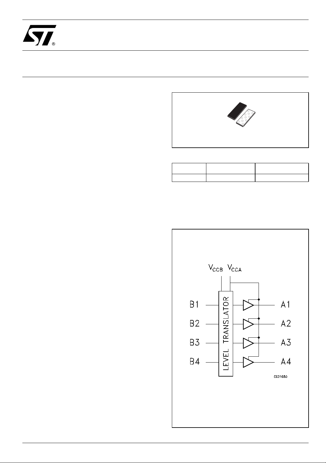
HS Compliant for FLIPCHIP Package
O
FLIPCHIP
Table 1: Order Codes
PACKAGE T & R Comments
FLIPCHIP11 ST4G3234BJR 5000 parts per reel
All inputs are equipped with protection circuits
against static discharge, giving them ESD immunity and transient excess voltage.
Figure 1: Logic Diagram
DESCRIPTION
The ST4G3234 is a dual supply low voltage
CMOS 4-BIT BUS BUFFER level translator
fabricated with sub-micron silicon gate and
five-layer metal wiring C
2
MOS technology.
Designed for use as an interface between a 3.3V
bus and a 2.5V or 1.8V bus in a mixed 3. 3V / 1.8V,
3.3V/2.5V, 1.8V/1.4V and 2.5V/1.8V supply
systems, it achieves high speed operation while
maintaining the CMOS low power dissipation.
This IC is intended for one-way asynchronous
communication between data buses. The input
and output power down protections disable the
device when both power supply are down, so that
the buses are effectively isolated.
The input tolerant buff ers allow to translate V
compatible signals and greater signals than V
up/down t o V
CCA
.
CCB
CCB
Rev. 7
1/11May 2005

ST4G3234
Figure 2: Input An d Output Equival e n t Ci rcuit
Table 2: Pin Description
PIN° SYMBOL NAME AND FUNCTION
A1 A4 Data Output
A3 A3 Data Output
A5 A2 Data Output
A7 A1 Data Output
C1 B4 Data Input
C3 B3 Data Input
C5 B2 Data Input
C7 B1 Data Input
B2 GND Ground (0V)
B6 V
B4 V
CCA
CCB
Positive Supply Voltage
Positive Supply Voltage
Figure 3: Pi n C onnect ion (top through view)
2/11
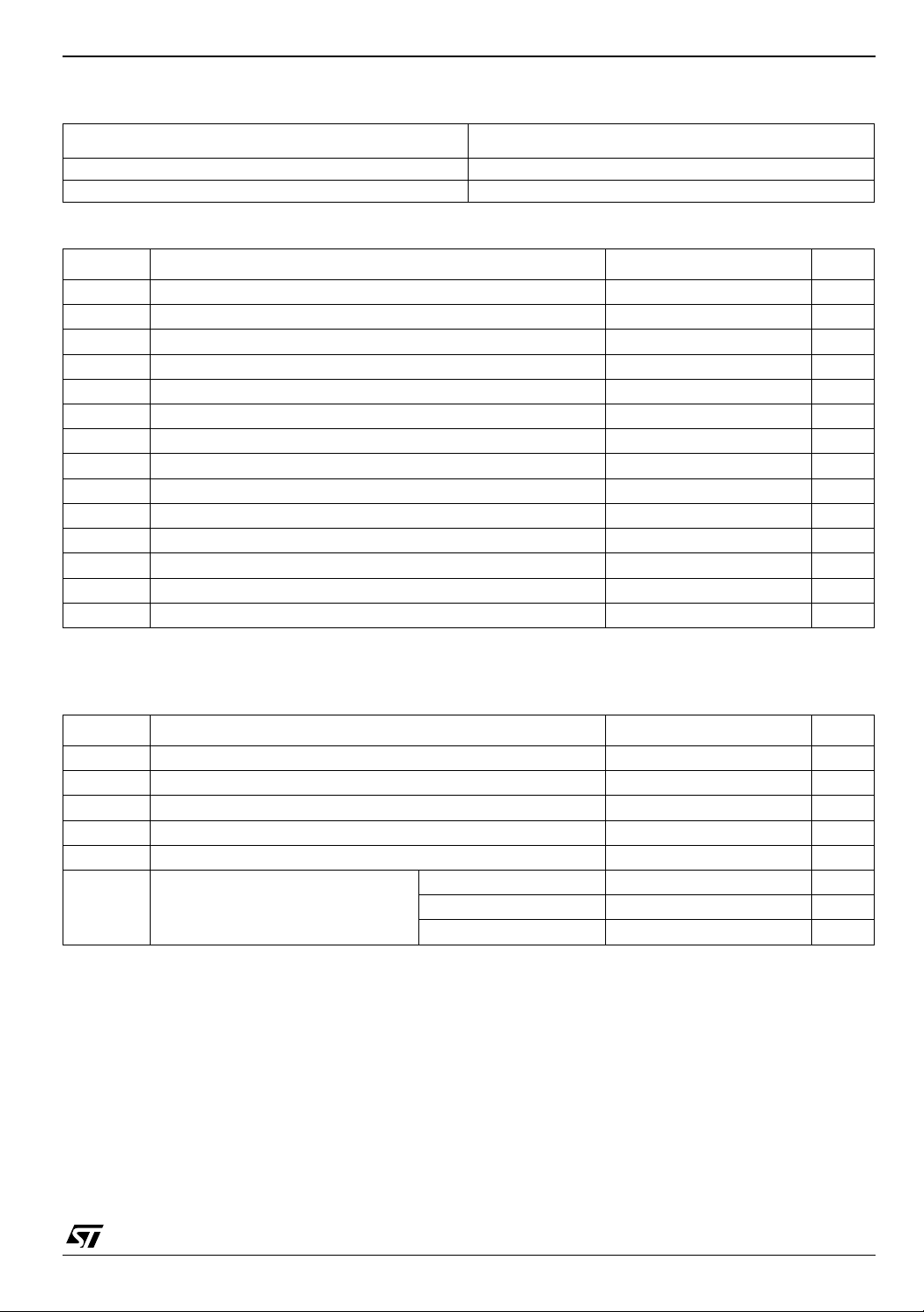
Table 3: Truth Ta ble
ST4G3234
INPUTS Bn (V
Referred) OUTPUTS Bn (V
CCB
Referred)
CCA
LL
HH
Table 4: Absolute Maximum Ratings
Symbol Parameter Value Unit
V
CCA
V
CCB
V
V
V
V
I
I
OK
I
OA
I
CCA
I
CCB
P
T
T
Absolute Maximum Ratings are those value beyond which damage to the device may occur. Functional operation under these conditions is
not implied
Output Supply Voltage
Input Supply Voltage
DC Output Voltage (Power Down Mode: V
OA
DC Input Voltage (Power Down Mode: V
IB
DC Output Voltage -0.5 to V
OA
DC Input Voltage
IB
DC Input Diode Current
IK
CCA=VCCB
CCA=VCCB
=Gnd)
=Gnd)
DC Output Diode Current
DC Output Current
DC V
DC V
Power Dissipation
d
Storage Temperature
stg
Lead Temperature (10 sec)
L
or Ground Current
CCA
or Ground Current
CCB
-0.5 to +4.6 V
-0.5 to +4.6 V
-0.5 to +4.6 V
-0.5 to +4.6 V
+ 0.5
CCA
-0.5 to +4.6 V
− 20 mA
− 50 mA
± 50 mA
± 100 mA
± 100 mA
400 mW
-65 to +150 °C
260 °C
V
Table 5: Recommended Operating Conditions
Symbol Parameter Value Unit
V
CCA
V
CCB
V
V
T
dt/dv
1) VI from 0.8V to 2.0V at V
Supply Voltage
Supply Voltage
Input Voltage (Bn) 0 to V
IB
Output Voltage (An) 0 to V
OA
Operating Temperature
op
Input Rise and Fall Time (note 1) V
= 3.0V
CC
= 3.0 to 3.6V
CCB
= 2.3 to 2.7V
V
CCB
V
= 1.4 to 1.95V
CCB
1.4 to 3.6 V
1.4 to 3.6 V
CCB
CCA
-40 to 85 °C
0 to 10 ns/V
0 to 20 ns/V
0 to 100 ns/V
V
V
3/11
ST4G3234
Table 6: DC Specification
Symbol Parameter
V
V
V
I
I
∆I
IHB
V
ILB
OHA
OLA
I
IB
I
OFF
CCtB
CCtA
CCtB
High Level Input
Voltage (Bn)
Low Level Input
Voltage (Bn)
High Level
Output Voltage
Low Level
Output Voltage
Input Leakage
Current
Power Off
Leakage Current
Quiescent
Supply Current
Quiescent
Supply Current
Maximum
Quiescent
Supply Current /
Input (Bn)
V
CCB
(V)(*)
1.4
1.8
2.5 1.6 1.6
3.3 2.0 2.0
1.4
1.8
2.5 0.7 0.7
3.3 0.8 0.8
1.4
to
3.6V
1.4
to
3.6V
2.7 3.6
1.4 2.7
00VIB=GND to 3.6V
1.4
to
3.6V
1.4
to
3.6V
2.7 3.6
1.95 3.6
1.95 2.7
Test Condition Value
= 25 °C
T
V
CCA
(V)(*)
1.4
to
Min. Typ. Max. Min. Max.
0.65V
0.65V
A
CCB
CCB
3.6V
0.35V
1.4
to
0.35V
3.6V
1.4 IO=-100µA
2.75 I
2.3
1.65
1.4
=-10mA
O
=-8mA
I
O
=-6mA
I
O
I
=-2mA
O
1.2 1.2
2.2 2.2
2.0 2.0
1.4 1.4
1.1 1.1
1.4 IO=100µA
2.75 I
2.3
1.65
1.4
=10mA
O
=8mA
I
O
I
=6mA
O
=2mA
I
O
=V
V
IB
CCB
=3.6V or GND
V
IB
or GND
0.55 0.55
0.30 0.30
0.25 0.25
0.20 0.20
± 0.5 ± 5 µA
± 0.5 ± 5 µA
± 1.0 ± 10 µA
V
=GND to 3.6V
OA
1.4
to
=V
CCB
or GND
V
IB
3.6V
1.4
to
=V
CCB
or GND
V
IB
3.6V
=V
CCB
CCB
- 0.6V
or GND
V
IB
V
=V
IB
CCB
CCB
-40 to 85 °C
0.65V
CCB
0.65V
CCB
0.35V
0.35V
CCB
CCB
Unit
V
V
V
0.2 0.2
V
0.5 5 µA
0.5 5 µA
0.75 mA
(*) VCC range = 3.3±0.3; 2.5 ±0.2V ; 1.8±0.15V
4/11

Table 7: Dynamic Switching Characteristics
Test Condition Value
Symbol Parameter
V
Dynamic Low Level
OLPA
Quiet An Output
V
CCB
(V)
1.4 1.8
V
CCA
(V)
1.8-2.5 3.3 0.35
V
Dynamic Low Level
OLVA
Quiet An Output
1.4 1.8
1.8-2.5 3.3 -0.35
V
OHVA
Dynamic High Level
Quiet An Output
1.4 1.8
1.8-2.5 3.3 2.7
Table 8: AC Electrical Characteristics
V
V
V
IL
IL
IL
= 25 °C
T
A
Min. Typ. Max. Min. Max.
=30pF
C
L
=0V V
C
=30pF
L
=0V V
C
=30pF
L
=0V V
IH =VCC
IH =VCC
IH =VCC
0.2
-0.2
1.6
Test Condition Value
ST4G3234
-40 to 85 °C
Unit
V1.4-1.8 2.5 0.25
V1.4-1.8 2.5 -0.25
V1.4-1.8 2.5 2.1
Symbol Parameter
Propagation Delay Time Bn to An 2.3 to 3.6 1.4
t
PLH
t
PHL
V
CCB
(V)
V
CCA
(V)
-40 to 85 °C
Min. Max.
2.0 5.5
1.4 to 1.95 1.4 2.0 5.5
Unit
2.3 to 3.6 1.65 to 1.95 2.0 5.0
1.4 to 1.95 1.65 to 1.95 2.0 5.2
CL = 10 pF
ns
1.4 to 1.95 2.3 to 2.7 2.0 4.6
1.4 to 1.95 3.0 to 3.6 2.0 4.3
2.3 to 2.7 3.0 to 3.6 1.0 3.5
t
Propagation Delay Time Bn to An 2.3 to 3.6 1.4
PLH
t
PHL
1.4 to 1.95 1.4 2.0 7.9
2.3 to 3.6 1.65 to 1.95 2.0 6.0
1.4 to 1.95 1.65 to 1.95 2.0 6.5
1.4 to 1.95 2.3 to 2.7 2.0 5.7
= 30 pF
C
L
R
= 500 Ω
L
2.0 7.5
ns
1.4 to 1.95 3.0 to 3.6 2.0 5.2
2.3 to 2.7 3.0 to 3.6 1.0 4.6
t
OSLH
t
OSHL
1) Skew is defined as the absolute value of the difference between the actual propagation delay for any two outputs of the same device switching in the sa me directio n, either HIG H or LOW (t
2) Param eter guaran teed by design
Output To Output Skew Time (note1, 2) 1.8 ± 0.15 2.5 ± 0.2
1.8 ± 0.15 3.3 ± 0.3 0.5
2.5 ± 0.2 3.3 ± 0.3 0.75
OSLH
= | t
PLHm
- t
PLHn
|, t
OSHL
= | t
PHLm
- t
PHLn
C
R
L
|
= 30 pF
L
= 500 Ω
0.5 ns
5/11

ST4G3234
Table 9: Capacitance Characteristics
Test Condition Value
= 25 °C
Symbol Parameter
C
C
Input Capacitance open open 7 pF
INB
Output Capacitance 2.5 3.3 9 pF
C
O
Power Dissipation
PD
Capacitance
V
V
CCB
CCA
(V)
(V)
2.5 3.3 f=10MHz 28
1.8 3.3 28
T
A
Min. Typ. Max. Min. Max.
1.4 2.5 25
1.4 1.8 21
3.3 1.8 28
1) CPD is defined as the value of the IC’s internal equivalent capacitance which is calculated from the operating current consumption without
load. (R efer to Test Circuit). Average curre nt can be obtained by the following equation. I
= CPD x VCC x fIN + ICC/4 (per circuit)
CC(opr)
Figure 4: Te st Circuit
-40 to 85 °C
Unit
pF
TEST SWITCH
, t
t
PLH
PHL
CL = 30pF or equivalent (includes jig and p robe capacitance)
R
= R1 = 500Ω or equivalent
L
= Z
R
of pulse generator (typically 50Ω)
T
OUT
Table 10: Waveform Symbol Value
6/11
Symbol
V
IH
V
M
V
X
V
Y
3.0 to 3.6V 2.3 to 2.7V 1.65 to 1.95V
V
CC
1.5V VCC/2 VCC/2
VOL +0.3V VOL +0.15V VOL +0.15V
VOL -0.3V VOL -0.15V VOL -0.15V
Open
V
CC
V
CC
V
CC

Figure 5: Waveform - Propagation Delay (f=1MHz; 50% duty cycle)
ST4G3234
Figure 6: Marking
NOTE: E = Eco Level; Y = Assy Year; WW = Assy Week; X = Marking Area; Marking Code 9521
7/11

ST4G3234
Flip-Chip11 MECHANICAL DATA
mm. mils
DIM.
MIN. TYP MAX. MIN. TYP. MAX.
A 0.585 0.65 0.715 23.0 25.6 28.1
A1 0.21 0.25 0.29 8.3 9.8 11.4
A2 0.40 15.7
b 0.265 0.315 0.365 10.4 12.4 14.4
D 1.992.042.0978.380.382.3
D1 1.5 59.1
E 1.361.411.4653.555.557.5
E1 0.866 34.1
eD 0.2 0.25 0.30 7.9 9.8 11.8
eE 0.383 0.433 0.483 15.1 17.0 19.0
fD 0.270 10.6
fE 0.272 10.7
ccc 0.080 3.1
8/11
7224724E

ST4G3234
Tape & Reel Flip-Chip 11 MECHANICAL DATA
mm. inch
DIM.
MIN. TYP MAX. MIN. TYP. MAX.
A 178 6.926
C 12.8 13.2 0.504 0.519
D 20.2 0.795
N 49 50 51 1.929 1.969 2.008
T 12.4 0.488
Ao 2.29 2.34 2.39 0.090 0.092 0.094
Bo 1.65 1.70 1.75 0.065 0.067 0.069
Ko 0.76 0.81 0.86 0.030 0.032 0.034
Po 3.9 4 4.1 0.153 0.157 0.161
P 3.9 4 4.1 0.153 0.157 0.161
9/11

ST4G3234
Table 11: Revision History
Date Revision Description of Changes
14-Oct-2004 1 First Release.
26-Oct-2004 2 Mechanical Data has been updated.
18-Nov-2004 3
11-Feb-2005 4 Add Tape & Reel and Figure 6.
18-Feb-2005 5 Table 1 has been updated from 4000 to 5000 parts per Reel.
18-Mar-2005 6 Add Features ==> Max Data Rates.
09-May-2005 7 Table 8 and Table 9 have been updated.
Mistake V
on table 6.
OHA
10/11

ST4G3234
Information furnished is believed to be accurate and reliable. However, STMicroelectronics assumes no responsibility for the consequences
of use of such information nor for any infringement of patents or other rights of third parties which may result from its use. No license is granted
by implic ati o n or ot h er wis e und er an y pat ent or pa te nt r igh ts of STMi cr oe l ect ro ni cs . Sp ec if i cat i on s ment i o ned i n th is p ub li c ati on ar e s ubj ec t
to change without notice. This publication supersedes and replaces all information previously suppli ed. STMicroelectronics products are not
authorized for use as critical components in life support devices or systems without express written approval of STMicroelectronics.
The ST logo is a registered trademark of STMicroelectronics
All other names are the property of their respective owners
© 2005 STMicroelectronics - All Rights Reserved
STMicroelectronics group of companies
Australia - Belgium - Brazil - Canada - China - Czech Republic - Finland - France - Germany - Hong Kong - India - Israel - Italy - Japan -
Malaysia - Malta - Morocco - Singapore - Spain - Sweden - Switzerland - United Kingdom - United States of America
www.st.com
11/11
 Loading...