

Datasheet ST491ACN, ST491ACDR, ST491ACD, ST491ABN, ST491ABD Datasheet (SGS Thomson Microelectronics)
Page 1
ST491A
LOW POWER HIGH SPEED RS-485/RS-422 TRANSCEIVER
■ LOW SUPPLY CURRENT: 5mA MAX
■ DESIGNED FOR RS485 INTERFACE
APPLICATIONS
■ -7 TO 12 COMMON MODE INPUT VOLTAGE
RANGE
■ 70mV TYPICAL INPUT HYSTERESIS
■ DESIGNED FOR 25Mbps OPERATION
■ OPERATE FROM SINGLE 5 SUPPLY
■ ±4kV ESD PROTECTION
■ CURRENT LIMITING AND T HER MAL
SHUTDOWN FOR DRIVER OVERLOAD
PROTECTION
DESCRIPTION
The ST491A is a low power transceiver for
RS-485 and RS-422 communications. The device
contains one driver and one receiver in full duplex
configuration. The ST491A draws 5mA (typ.) of
supply current when unloaded a nd operates from
a single 5V supply.
Driver is short-circuit current limited and is
protected against ex cessive power dissipation by
thermal shutdown circuitry that place the driver
outputs into a high-impedance state. The receiver
input has a fail-safe feature that guarantees a
logic high out put if both inputs are open circuit.
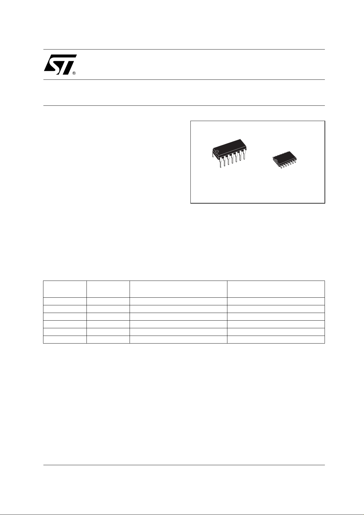
DIP SOP
ORDERING CODES
Type
ST491ACN 0 to 70 °C DIP-14 25parts per tube /40tube per box
ST491ABN -40 to 85 °C DIP-14 25parts per tube / 40tube per box
ST491ACD 0 to 70 °C SO-14 (Tube) 50parts per tube / 20tube per box
ST491ABD -40 to 85 °C SO-14 (Tube) 50parts per tube / 20tube per box
ST491ACDR 0 to 70 °C SO-14 (Tape & Reel) 2500 parts per reel
ST491ABDR -40 to 85 °C SO-14 (Tape & Reel) 2500 parts per reel
Temperature
Range
Package Comments
1/12July 2003
Page 2
ST491A
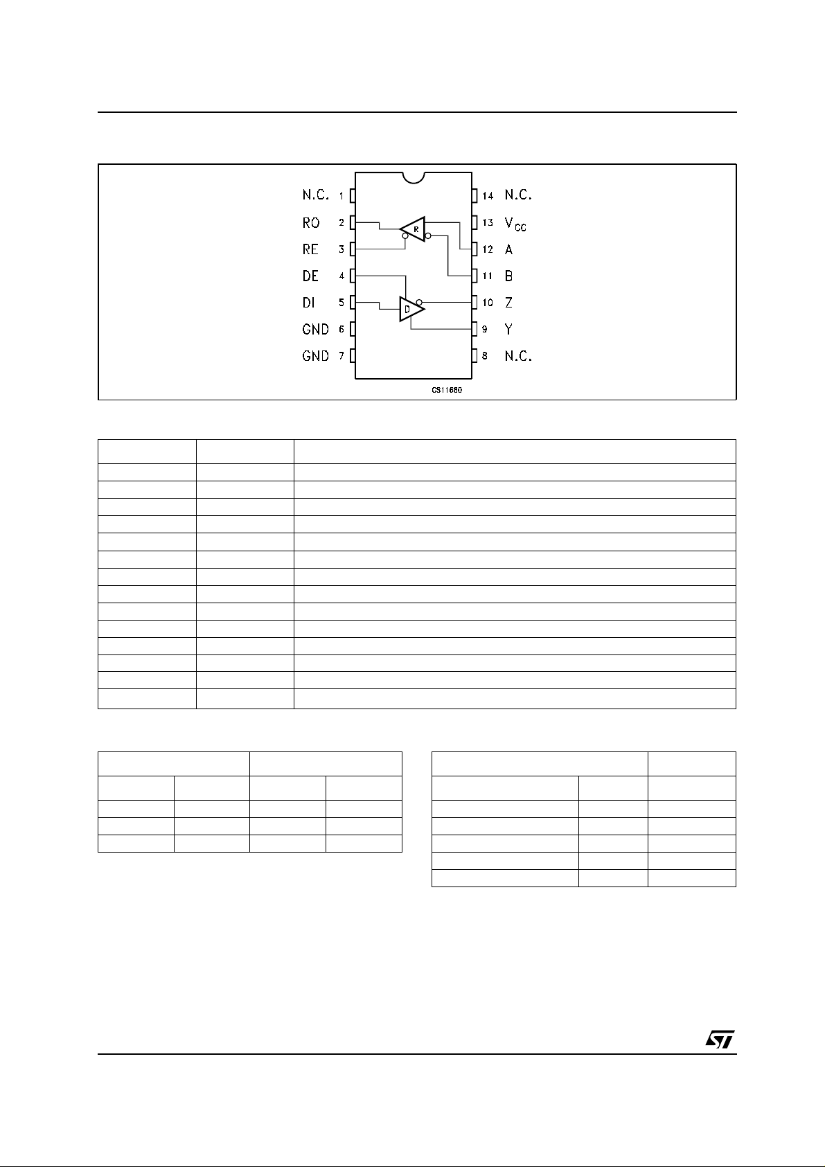
PIN CONFIGURA TION
PIN DESCRIPTION
PlN N° SYMBOL NAME AND FUNCTION
1 NC Not Connected
2 RO Receiver Output.
3 RE Receiver Output Enable
4 DE Driver Output Enable
5 DI Inverting Driver Input.
6 GND Ground
7 GND Ground
8 NC Not Connected
9 Y Non-inverting Driver Output
10 Z Inverting Driver Output
11 B Inverting Receiver Input
12 A Non-inverting Receiver Input
13 NC Not Connected
14
V
CC
Supply Voltage
TRUTH TABLE (DRIVER)
INPUT OUTPUTS
DI DE Y Z
LHLH
HHHL
XLZZ
X= Don’t Care; Z=High Impedance
2/12
TRUTH TABLE (RECEIVER)
INPUT OUTPUT
A-B RE RO
≥ -0.2V L H
between -0.2V to 0.2V L ?
≤ -0.2V L L
OPEN L H
XHZ
?= Irrelevant; X= Don’t Care; Z=High Impedance
Page 3
ST491A
ABSOLUTE MAXIMUM RATINGS
Symbol Parameter Value Unit
V
V
V
Y,VZ
V
A,VB
V
RO
ESD Human Body Model 3.5 KV
Absolute Maximum Ratings are those values beyond which damage to the device may occur. Functional operation under these condition is
not implied.
ELECTRICAL CHARACTERISTICS
V
=4.5Vto5.5V,TA=-40to85°C, unless otherwise specified.TypicalvaluesarereferredtoTA=25°C)
CC
Symbol Parameter Test Conditions Min. Typ. Max. Unit
I
SUPPLY
C
IN
C
YZ
C
OUT
Supply Voltage
CC
Driver Input Voltage
DI
Driver Output Voltage
Receiver Input Voltage
7V
-0.5 to 7 V
-7.5 to 12.5 V
-7.5 to 12.5 V
Receiver Output Voltage -0.3 to (VCC+ 0.3)
No Load Supply Current 2 5 mA
Input Capacitance 1.8 pF
Driver Output Capacitance 1.2 pF
Output Capacitance 2.3 pF
V
TRANSMITTER ELECTRICAL CHARACTERISTICS
V
=4.5Vto5.5V,TA= -40 to 85°C,unless oth erwise specified. Typical v alues arereferred to Ta= 25°C)
CC
Symbol Parameter Test Conditions Min. Typ. Max. Unit
V
V
V
∆V
V
∆V
I
I
OSD
V
Differential Drive Output
OD1
(No load)
Differential Drive Output
OD2
(With Load)
Differential Drive Output
OD3
(With Load)
Change in magnitude of
OD
Driver Differential Output
RL=54Ω(RS-422) (Figure 1) 1.5 2.6 5 V
RL= 100Ω (RS-422) (Figure 1) 2 3 V
=54Ωor 100Ω (Figure 1) 0 0.2 V
R
L
Voltage for Complementary
Output States (Note1)
Driver Common Mode
OC
Output Voltage
Change in magnitude of
OC
Driver Common Mode
RL=54Ω(Figure 1) 1 3 V
=54Ω(Figure 1) 0 0.2 V
R
L
Output Voltage (Note1)
Power Off Output Current VCC=0V VO=-7V to 12V ± 100 µA
OFF
Driver Short Circuit Output
VO=-7V to 12V ± 35 ± 250 mA
Current
V
Input Logic Threshold Low 0.8 V
IL
Input Logic Threshold High 2 V
IH
V
CC
V
3/12
Page 4
ST491A
RECEIVER ELECTRICAL CHARACTERISTICS
V
=4.5Vto5.5V,TA= -40 to 85°C,unless oth erwise specified. Typical v alues arereferred to Ta= 25°C)
CC
Symbol Parameter Test Conditions Min. Typ. Max. Unit
I
Input Current (A, B) other input=0V
V
∆V
V
V
R
IN
Receiver Differential
TH
Threshold Voltage
Receiver Input Hysteresis VCM=0V 70 mV
TH
Receiver Output High
OH
Voltage
Receiver Output Low
OL
Voltage
Receiver Input Resistance VCM= -7V to 12V 12 24 KΩ
RIN
= 0 or 5.25V
V
CC
VCM= -7V to 12V -0.2 0.2 V
I
= -8mA, VID= 200mV 3.5 4.7 V
OUT
I
= 8mA, VID= -200mV 0.3 0.5 V
OUT
DRIVER SWITCHING CHARACTERISTICS
=4.5Vto5.5V,TA=-40to 85°C, unlessotherwise specified. Typicalvalues are referred toTa=25°C)
V
CC
Symbol Parameter Test Conditions Min. Typ. Max. Unit
Maximum Data Rate Jitter <5% 25 50 Mbps
D
R
t
PLH
t
PHL
t
SKEW
t
TLH
t
THL
t
PZL
t
PZH
t
PHZ
t
PLZ
Propagation Delay Input to
Output
Differential Output Delay
Skew
Rise or Fall Differential
Time
Output Enable Time CL= 50pF S1 Closed 14 25 ns
Output Enable Time CL= 50pF S2 Closed 14 25 ns
Output Disable Time CL= 15pF S2 Closed 10 25 ns
Output Disable Time CL= 15pF S1 Closed 16 25 ns
RL=54Ω CL1=CL2=50pF, (Figure 1) 10 16 ns
RL=54Ω CL1=CL2=50pF, (Figure 1) 1 3 ns
RL=54Ω CL1=CL2=50pF, (Figure 1) 8 12 ns
V
=12V 0.5 1 mA
IN
=-7V -0.35 -0.8 mA
V
IN
RECEIVER SWITCHING CHARACTERISTICS
=4.5Vto5.5V,TA=-40to85°C, unless otherwisespecified.Typicalvalues are ref erred toTa=25°C)
V
CC
Symbol Parameter Test Conditions Min. Typ. Max. Unit
Propagation Delay Input to
t
PLH
Output
t
PHL
t
SKD|tPLH -tPHL
Skew
t
t
t
t
Rise or Fall Time CL= 15pF (Figures 2,4) 6 ns
TLH
THL
Output Enable Time CRL= 15pF S1 Closed 6 12 ns
t
PZL
Output Enable Time CRL= 15pF S2 Closed 7 12 ns
PZH
Output Disable Time CRL= 15pF S2 Closed 6 12 ns
PHZ
Output Disable Time CRL= 15pF S1 Closed 6 12 ns
t
PLZ
4/12
| Receiver Output
CL= 15pF (Figures 2,4) 19 30 ns
CL= 15pF (Figures 2,4) 1 3 ns
Page 5

TEST CIRCUITS AND TYPICAL CHARA CTERISTICS
Figure1 : Driver DC Test Load
Figure2 : Receiver Timing Test Load
ST491A
Figure3 : Driver/Receiver Timing Test Circuit
5/12
Page 6

ST491A
Figure4 : Driver Timing Test Load
Figure5 : Driver Propagation Delay
6/12
Page 7

Figure6 : Receiver Propagation Delay
ST491A
Figure7 : Receiver Output Current vs Output
Voltage (Output Low)
Figure8 : Receiver Output Current vs Output
Voltage (Outpu t High)
Figure9 : Driver Diff. Output Voltage vs Common
Mode Voltage (Diff. Output Low)
Figure10 : Driver Diff. Output Voltage vs
Common Mode Voltage (Diff. Output High)
7/12
Page 8

ST491A
Figure11 : Driver Short Circuit Current vs Line
Voltage (Outpu t High)
Figure12 : Driver Short Circuit Current vs. Li ne
Voltage (Output Low)
Figure13 : Receiver Input Current vs Input
Voltage
8/12
Page 9

Plastic DIP-14 MECHANICAL DATA
mm. inch
DIM.
MIN. TYP MAX. MIN. TYP. MAX.
a1 0.51 0.020
B 1.39 1.65 0.055 0.065
b 0.5 0.020
b1 0.25 0.010
D 20 0.787
E 8.5 0.335
e 2.54 0.100
e3 15.24 0.600
F 7.1 0.280
ST491A
I 5.1 0.201
L 3.3 0.130
Z 1.27 2.54 0.050 0.100
P001A
9/12
Page 10

ST491A
SO-14 MECHANICAL DATA
DIM.
A 1.75 0.068
a1 0.1 0.2 0.003 0.007
a2 1.65 0.064
b 0.35 0.46 0.013 0.018
b1 0.19 0.25 0.007 0.010
C 0.5 0.019
c1 45˚ (typ.)
D 8.55 8.75 0.336 0.344
E 5.8 6.2 0.228 0.244
e 1.27 0.050
e3 7.62 0.300
F 3.8 4.0 0.149 0.157
G 4.6 5.3 0.181 0.208
L 0.5 1.27 0.019 0.050
M 0.68 0.026
S ˚ (max.)
MIN. TYP MAX. MIN. TYP. MAX.
mm. inch
8
10/12
PO13G
Page 11

ST491A
Tape & Reel SO-14 MECHANICAL DATA
mm. inch
DIM.
MIN. TYP MAX. MIN. TYP. MAX.
A 330 12.992
C 12.8 13.2 0.504 0.519
D 20.2 0.795
N 60 2.362
T 22.4 0.882
Ao 6.4 6.6 0.252 0.260
Bo 9 9.2 0.354 0.362
Ko 2.1 2.3 0.082 0.090
Po 3.9 4.1 0.153 0.161
P 7.9 8.1 0.311 0.319
11/12
Page 12

ST491A
Information furnished is believed to be accurate and reliable. However, STMicroelectronics assumes no responsibility for the
consequences of use o f suc h inf ormat ion n or f or an y infr ingeme nt of paten ts or oth er ri gh ts of third part ies whic h may resul t f rom
its use. No license is granted by implication or otherwise under any patent or patent rights of STMicroelectronics. Specifications
mentioned in this publication are subject to change without notice. This publication supersedes and replaces all information
previously supplied. STMicroelectronics products are not authorized for use as critical components in life support devices or
systems without express written approval of STMicroelectronics.
Australia - Brazil - Canada - China - Finland - France - Germany - Hong Kong - India - Israel - Italy - Japan - Malaysia - Malta - Morocco
© The ST logo is a registered trademark of STMicroelectronics
© 2003 STMicroelectronics - Printed in Italy - All Rights Reserved
STMicroelectronics GROUP OF COMPANIES
Singapore - Spain - Sweden - Switzerland - United Kingdom - United States.
© http://www.st.com
12/12
 Loading...