

Page 1
Features
■ Low quiescent current: 300 µA
■ Designed for RS-485 interface application
■ - 7 V to 12 V common mode input voltage range
■ Driver maintains high impedance in 3-state or
with the power OFF
■ 70 mV typical input hysteresis
■ 30 ns propagation delay, 5 ns skew
■ Operate from a single 5 V supply
■ Current limiting and thermal shutdown for
driver overload protection
■ ESD protection:
– ± 15 kV (HBM)
– ± 8 kV (IEC-1000-4-2 contact discharge)
■ Allows up to 256 transceivers on the bus
ST485ERB
±15 kV ESD protected, low power
RS-485/RS-422 transceiver
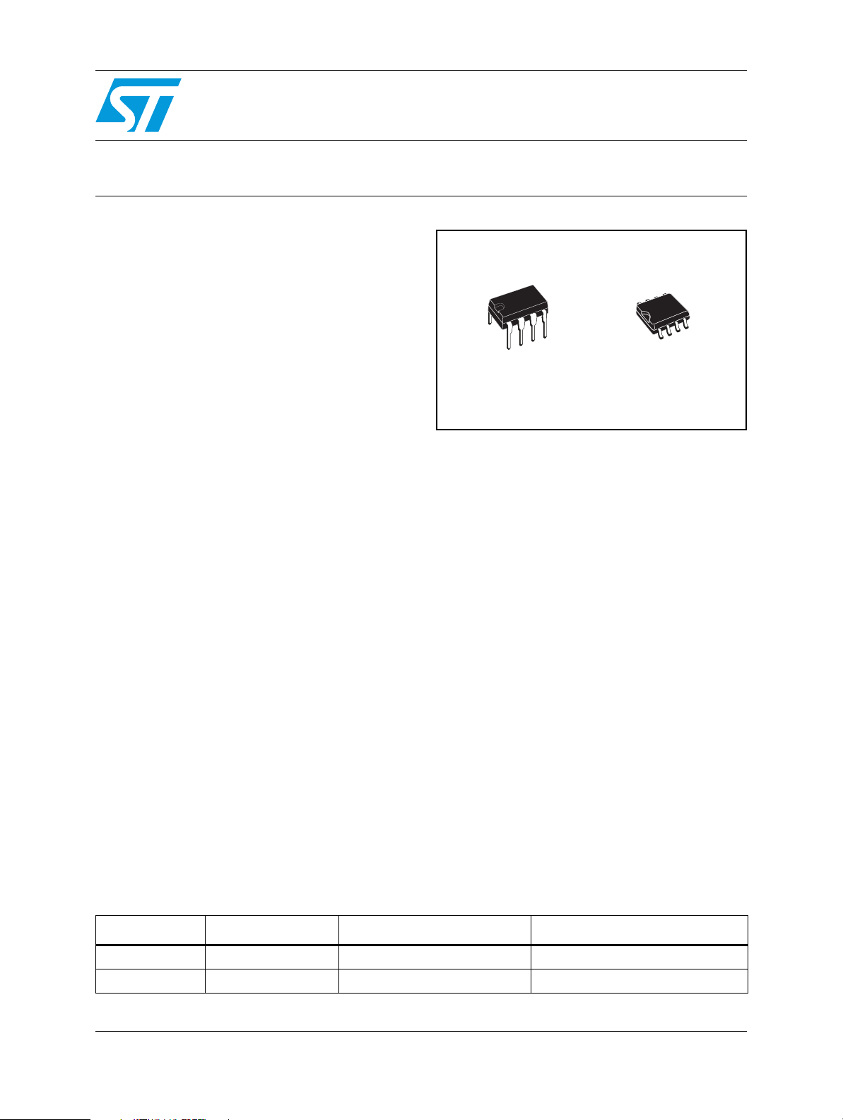
DIP-8 SO-8
The ST485ERB is designed for bi-directional data
communications on multipoint bus transmission
line (half-duplex applications).
Description
The ST485ERB is al low power transceiver for
RS-485 and RS-422 communication. Each driver
output and receiver input is protected against ±15
kV electrostatic discharge (HBM) ± 8 kV (IEC1000-4-2 contact discharge) shocks, without
latch-up. These parts contain one driver and one
receiver.
This transceiver draws 300 µA (typ.) of supply
current when unloaded or fully loaded with
disabled drivers.
It operates from a single 5 V supply.
Driver is short-circuit current limited and is
protected against excessive power dissipation by
thermal shutdown circuitry that places the driver
outputs into a high-impedance state.
Table 1. Device summary
Order code Temperature range Package Packaging
ST485ERBN - 40 to 85 °C DIP-8 50 parts per tube / 40 tube per box
ST485ERBDR - 40 to 85 °C SO-8 (tape and reel) 2500 parts per reel
February 2009 Rev 7 1/19
www.st.com
19
Page 2

Contents ST485ERB
Contents
1 Pin settings . . . . . . . . . . . . . . . . . . . . . . . . . . . . . . . . . . . . . . . . . . . . . . . . 3
2 Truth tables . . . . . . . . . . . . . . . . . . . . . . . . . . . . . . . . . . . . . . . . . . . . . . . . 4
3 Maximum ratings . . . . . . . . . . . . . . . . . . . . . . . . . . . . . . . . . . . . . . . . . . . . 5
4 Electrical characteristics . . . . . . . . . . . . . . . . . . . . . . . . . . . . . . . . . . . . . 6
5 Test circuit and typical characteristics . . . . . . . . . . . . . . . . . . . . . . . . . . 9
6 Package mechanical data . . . . . . . . . . . . . . . . . . . . . . . . . . . . . . . . . . . . 14
7 Revision history . . . . . . . . . . . . . . . . . . . . . . . . . . . . . . . . . . . . . . . . . . . 18
2/19
Page 3
ST485ERB Pin settings
1 Pin settings
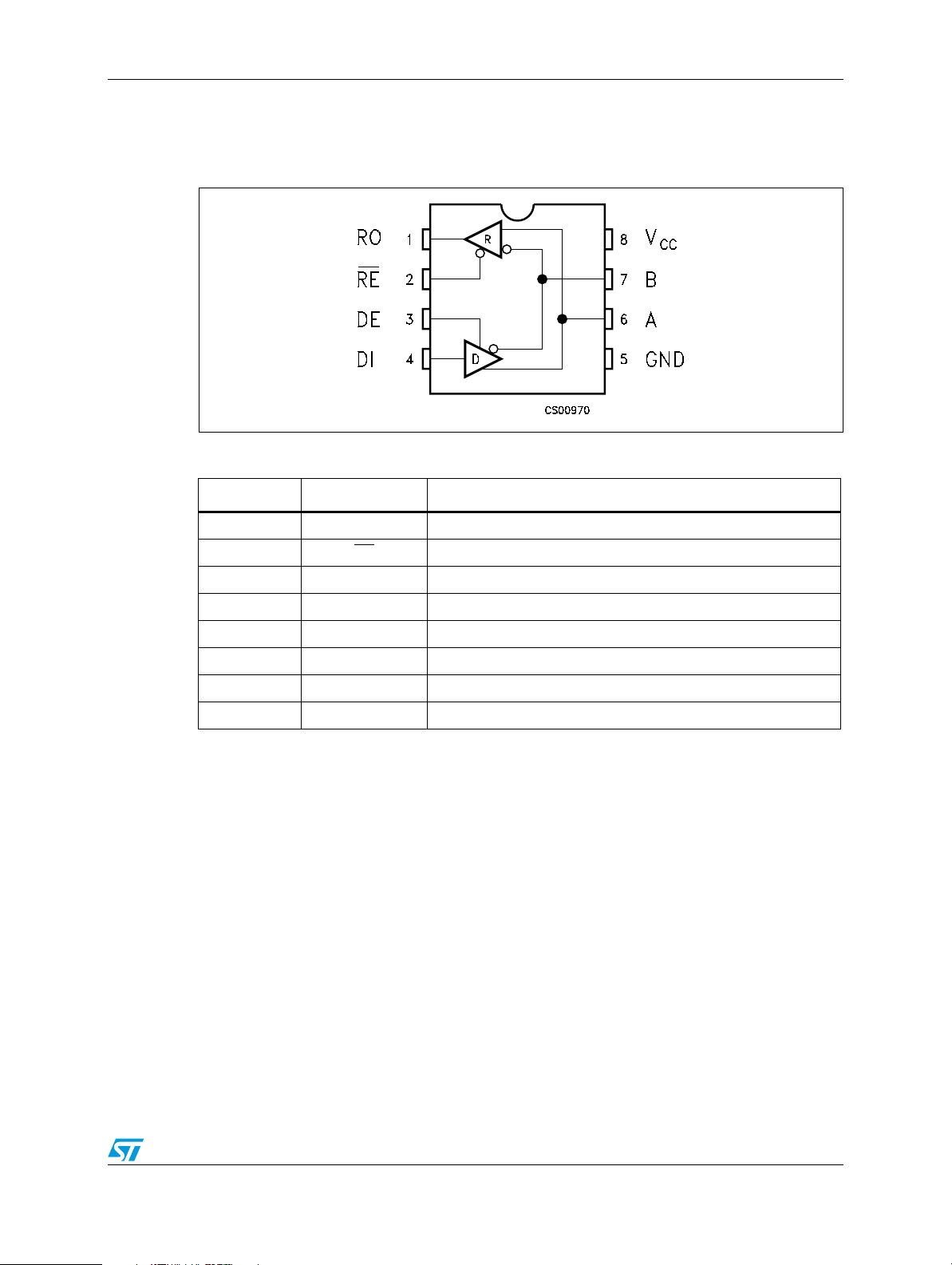
Figure 1. Pin configuration
Table 2. Pin description
Pin n° Symbol Name and function
1 RO Receiver output
2REReceiver output enable
3 DE Driver output enable
4 DI Driver input
5 GND Ground
6 A Non-inverting receiver input and non-inverting driver output
7 B Inverting receiver input and inverting driver output
8V
CC
Supply voltage
3/19
Page 4
Truth tables ST485ERB
2 Truth tables
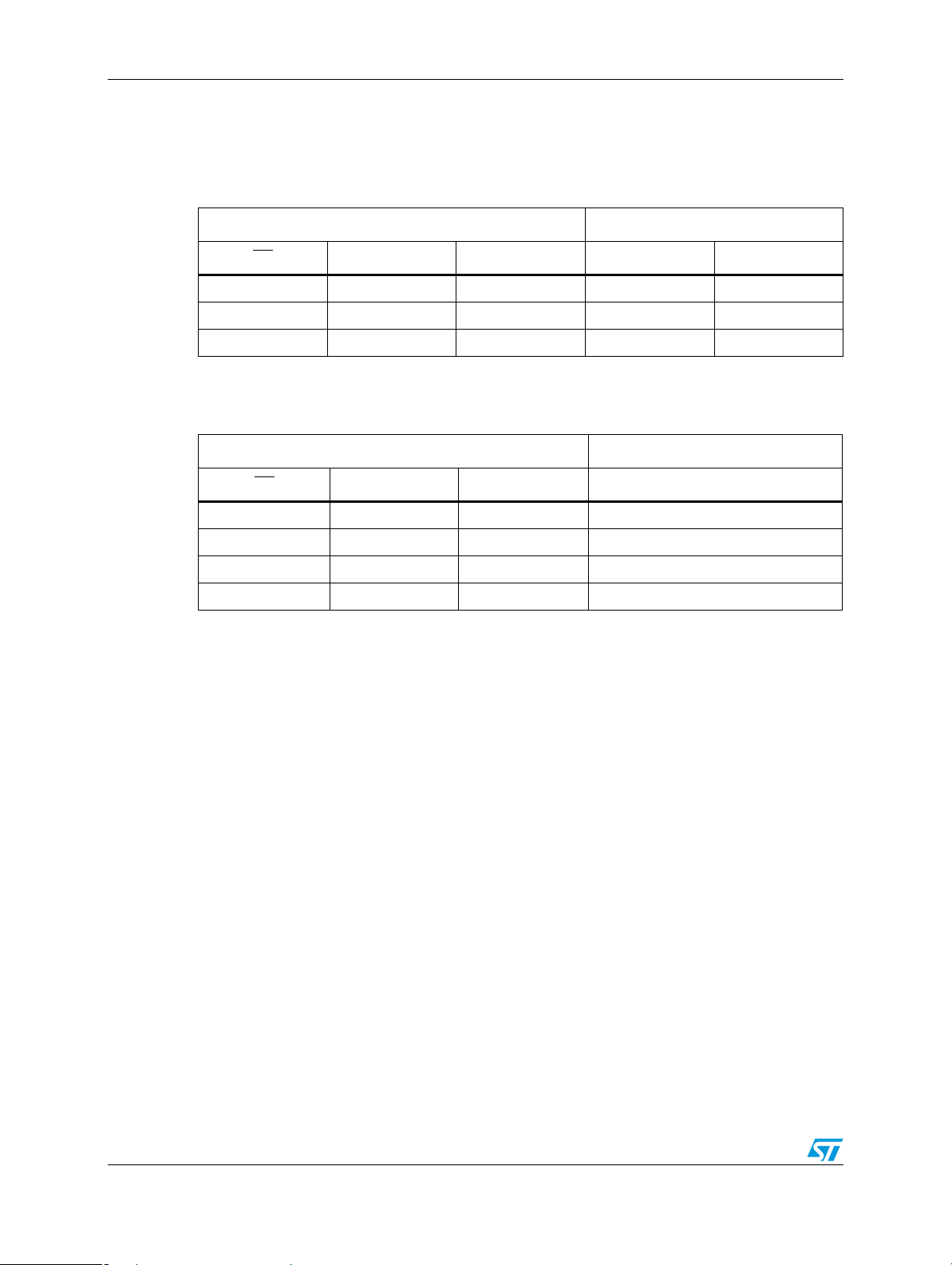
Table 3. Truth table (driver)
Inputs Outputs
RE
XHHLH
XHLHL
XLXZZ
DE DI B A
Note: X = Don’t care; Z = High impedance
Table 4. Truth table (receiver)
Inputs Outputs
RE
LL
LL
L L Inputs open H
HLX Z
DE A-B RO
Note: X = Don’t care; Z = High impedance
≥ +0.2V H
≤ -0.2V L
4/19
Page 5
ST485ERB Maximum ratings
3 Maximum ratings
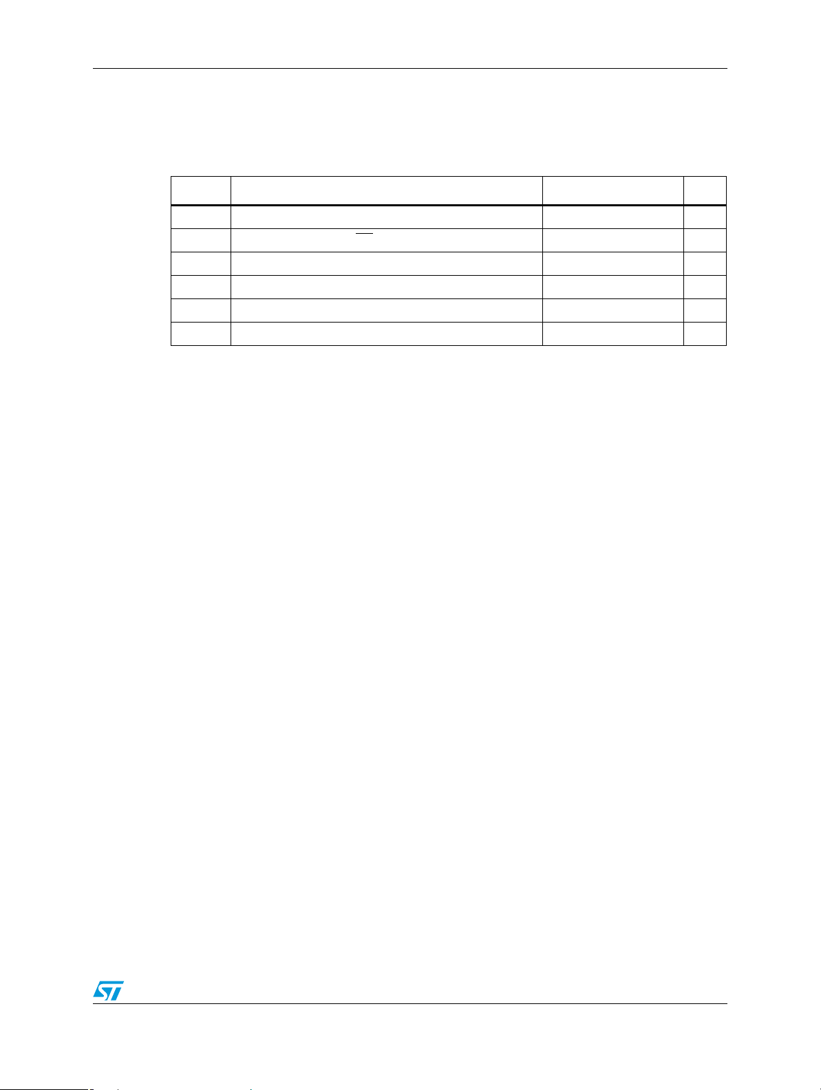
Table 5. Absolute maximum ratings
Symbol Parameter Value Unit
V
V
V
V
V
Supply voltage 7 V
CC
V
Control input voltage (RE, DE) -0.5 to (VCC + 0.5) V
I
Driver input voltage (DI) -0.5 to (VCC + 0.5) V
DI
Driver output voltage (A, B) ± 14 V
DO
Receiver input voltage (A, B) ± 14 V
RI
Receiver output voltage (RO) -0.5 to (VCC + 0.5) V
RO
Note: Absolute maximum ratings are those values beyond which damage to the device may occur.
Functional operation under these condition is not implied.
5/19
Page 6
Electrical characteristics ST485ERB
4 Electrical characteristics
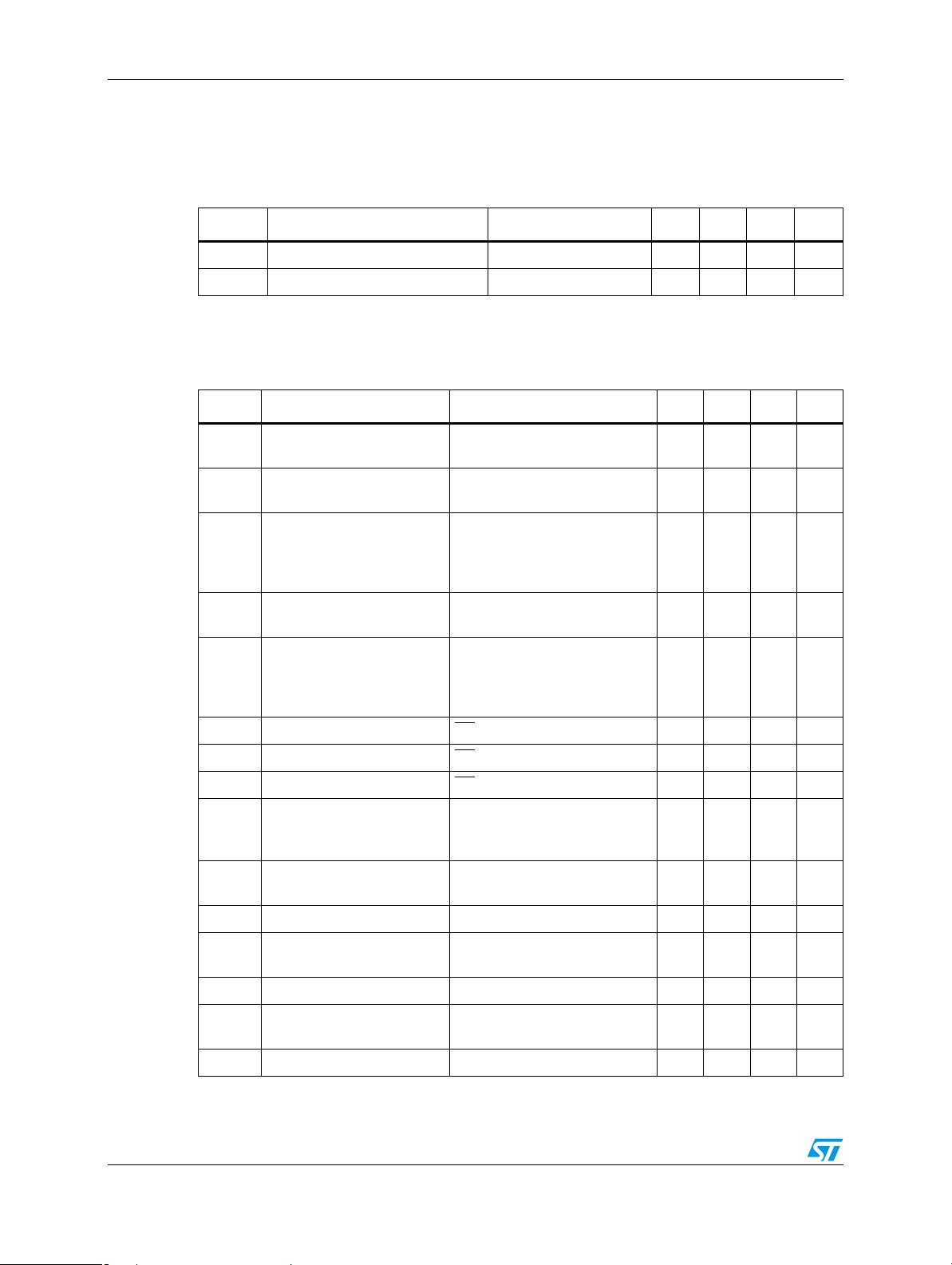
Table 6. ESD performance: transmitter outputs, receiver inputs
Symbol Parameter Test conditions Min. Typ. Max. Unit
ESD ESD protection voltage Human body model ±15 kV
ESD ESD protection voltage IEC-1000-4-2 ±8kV
VCC = 5 V ± 5 %, TA = T
to T
= 25 °C
A
Table 7. DC electrical characteristics
MIN
to T
, unless otherwise specified. Typical values are referred
MAX
Symbol Parameter Test conditions
V
V
Differential driver output (no
OD1
load)
Differential driver output
OD2
(with load)
RL = 27Ω (RS-485) (Figure 2)
= 50Ω (RS-422) (Figure 2)
R
L
Change in magnitude of
ΔV
driver differential output
OD
voltage for complementary
= 27Ω or 50Ω (Figure 2)0.2V
R
L
output states
V
Driver common-mode
OC
output voltage
= 27Ω or 50Ω (Figure 2)3V
R
L
Change in magnitude of
ΔV
driver common-mode output
OC
voltage for complementary
= 27Ω or 50Ω (Figure 2)0.2V
R
L
output states
V
Input high voltage RE, DE, DI 2.0 V
IH
V
Input low voltage RE, DE, DI 0.8 V
IL
I
I
V
ΔV
V
V
I
R
Input current RE, DE, DI ± 2µA
IN1
V
= 0V or 5.25V, VDE = 0V
Input current (A, B)
IN2
Receiver differential
TH
threshold voltage
Receiver input hysteresis VCM = 0V 70 mV
TH
Receiver output high
OH
voltage
Receiver output low voltage IO = 4mA, VID = -200mV 0.4 V
OL
3-State (high impedance)
OZR
output current at receiver
Receiver input resistance VCM = -7 to 12V 24 kΩ
IN
CM
= 12V
V
IN
V
= -7V
IN
= -7 to 12V -0.2 0.2 V
V
CM
= -4mA, VID = 200mV 3.5 V
I
O
= 0.4 to 2.4V ± 1µA
V
O
(1)
Min. Typ. Max. Unit
5V
5
1.5
V
5
V
1
-0.8mAmA
6/19
Page 7
ST485ERB Electrical characteristics
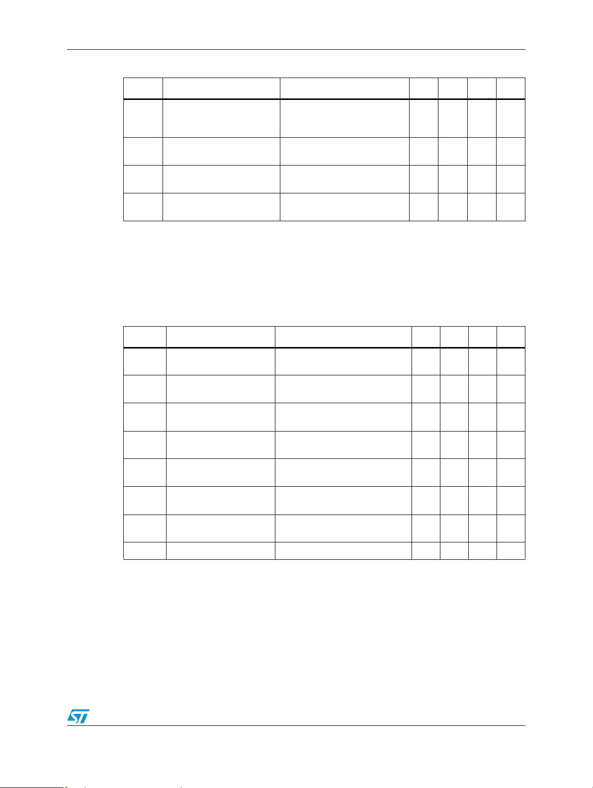
Table 7. DC electrical characteristics (continued)
Symbol Parameter Test conditions
(1)
Min. Typ. Max. Unit
VRE = 0V or V
I
No load supply current
CC
(2)
VDE = V
VDE = 0V
I
OSD1
I
OSD2
I
1. All currents into device pins are positive; all cuttents out of device pins are negative; all voltages are
2. Supply current specification is valid for loaded transmitters when V
3. Applies to peak current. See typical Operating Characteristics.
(VCC = 5 V ± 5 %, TA = T
to T
Table 8. Driver switching characteristics
Driver short-circuit current,
=High
V
O
Driver short-circuit current,
VO=Low
Receiver short-circuit
OSR
current
referenced to device ground unless specified.
to T
= 25 °C)
A
MIN
V
= -7 to 12V
O
= -7 to 12V
V
O
= 0V to V
V
O
, unless otherwise specified. Typical values are referred
MAX
Symbol Parameter Test conditions
t
t
t
t
t
PLH
t
TLH
THL
PZH
Propagation delay input to
output
PHL
Output skew to output
SK
Rise or fall time
Output enable time
R
= 54Ω, CL1 = CL2 = 100pF
DIFF
(see Figure 4 and Figure 6)
R
= 54Ω, CL1 = CL2 = 100pF
DIFF
(see Figure 4 and Figure 6)
= 54Ω, CL1 = CL2 = 100pF
R
DIFF
(see Figure 4 and Figure 6)
= 100pF, S2 = Closed
C
L
(see Figure 5 and Figure 7)
CC
CC
CC
(3)
(3)
DE
(1)
= 0 V
400
900
300
500µAµA
35 250 mA
35 250 mA
795mA
Min. Typ. Max. Unit
10 30 60 ns
510ns
31540ns
70 90 ns
C
= 100pF, S1 = Closed
t
t
t
PHZ
C
1. All currents into device pins are positive; all cuttents out of device pins are negative; all voltages are
referenced to device ground unless specified.
Output enable time
PZL
Output disable time
PLZ
Output disable time
Output AB capacitance 43 pF
AB
L
(see Figure 5 and Figure 7)
= 15pF, S1 = Closed
C
L
(see Figure 5 and Figure 7)
= 15pF, S2 = Closed
C
L
(see Figure 5 and Figure 7)
70 90 ns
70 90 ns
70 90 ns
7/19
Page 8
Electrical characteristics ST485ERB
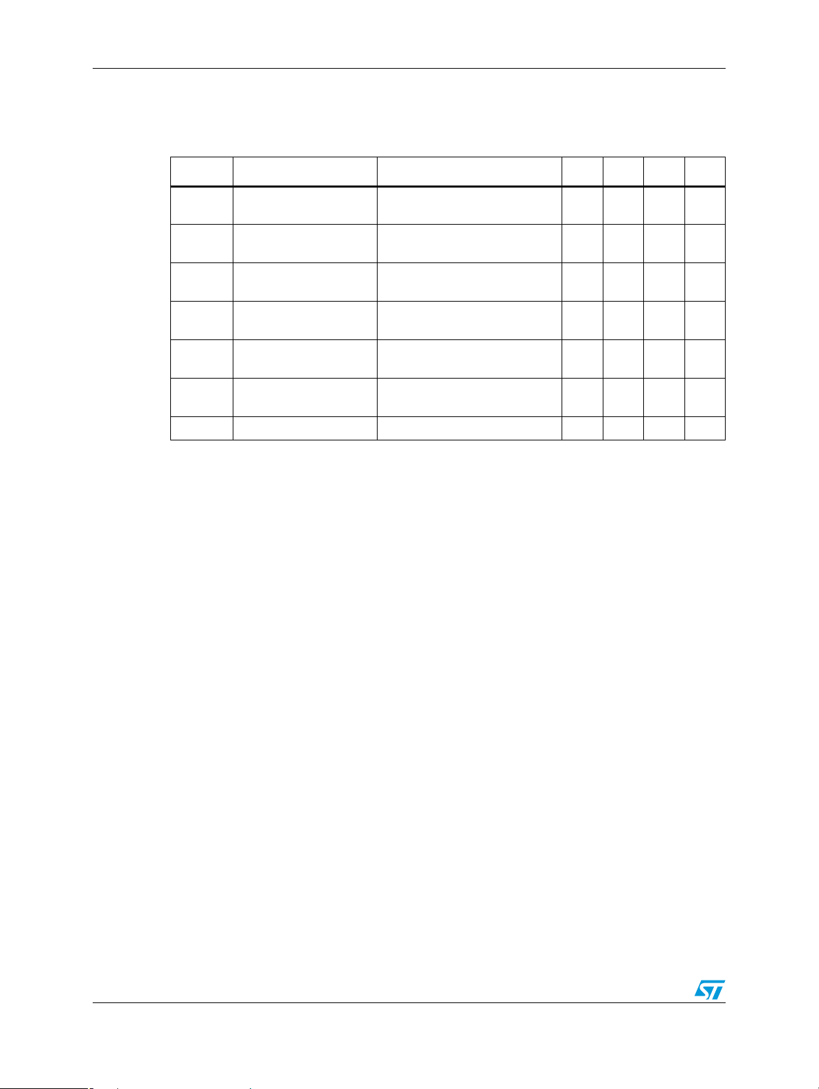
(VCC = 5 V ± 5 %, TA = T
to T
= 25 °C)
A
Table 9. Receiver switching characteristics
Symbol Parameter Test conditions
t
PLH
t
PHL
t
SKD
t
PZH
t
PZL
t
PLZ
t
PHZ
f
MAX
1. All currents into device pins are positive; all cuttents out of device pins are negative; all voltages are
referenced to device ground unless specified
Propagation delay input
to output
Differential receiver
skew
Output enable time
Output enable time
Output disable time
Output disable time
Maximum data rate 2.5 Mbps
MIN
to T
, unless otherwise specified. Typical values are referred
MAX
(1)
R
= 54Ω,CL1 = CL2 = 100pF
DIFF
(see Figure 4 and Figure 8)
R
= 54Ω, CL1 = CL2 = 100pF
DIFF
(see Figure 4 and Figure 8)
= 15pF, S1 = Closed (see
C
RL
Figure 2 and Figure 9)
= 15pF, S2 = Closed
C
RL
(see Figure 2 and Figure 9)
C
= 15pF, S1 = Closed
RL
(see Figure 2 and Figure 9)
= 15pF, S2 = Closed
C
RL
(see Figure 2 and Figure 9)
Min. Typ. Max. Unit
20 130 210 ns
13 ns
20 50 ns
20 50 ns
20 50 ns
20 50 ns
8/19
Page 9
ST485ERB Test circuit and typical characteristics
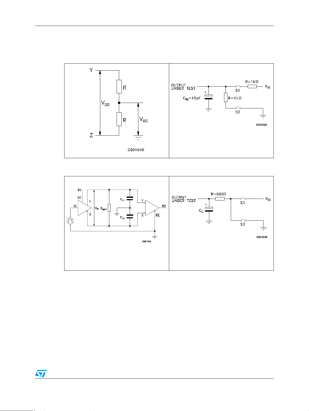
5 Test circuit and typical characteristics
Figure 2. Driver DC test load Figure 3. Receiver timing test load
Figure 4. Drive/receiver timing test
circuit
Figure 5. Driver timing test load
9/19
Page 10
Test circuit and typical characteristics ST485ERB
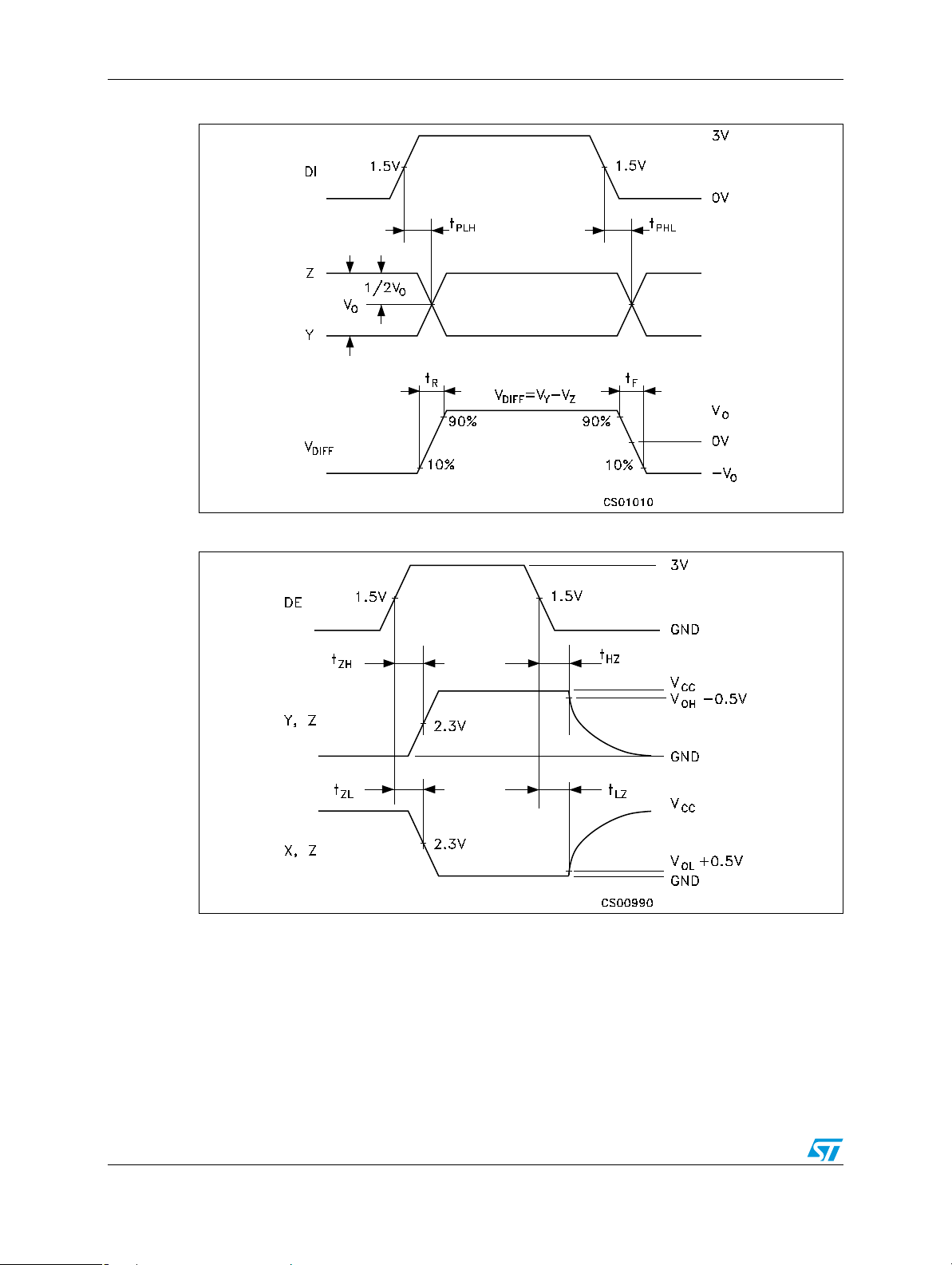
Figure 6. Driver propagation delay
Figure 7. Driver enable and disable time
10/19
Page 11
ST485ERB Test circuit and typical characteristics
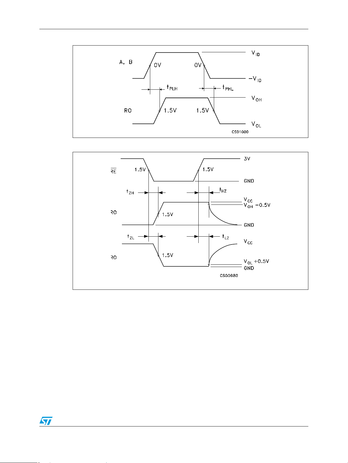
Figure 8. Receiver propagation delay
Figure 9. Receiver enable and disable time
11/19
Page 12
Test circuit and typical characteristics ST485ERB
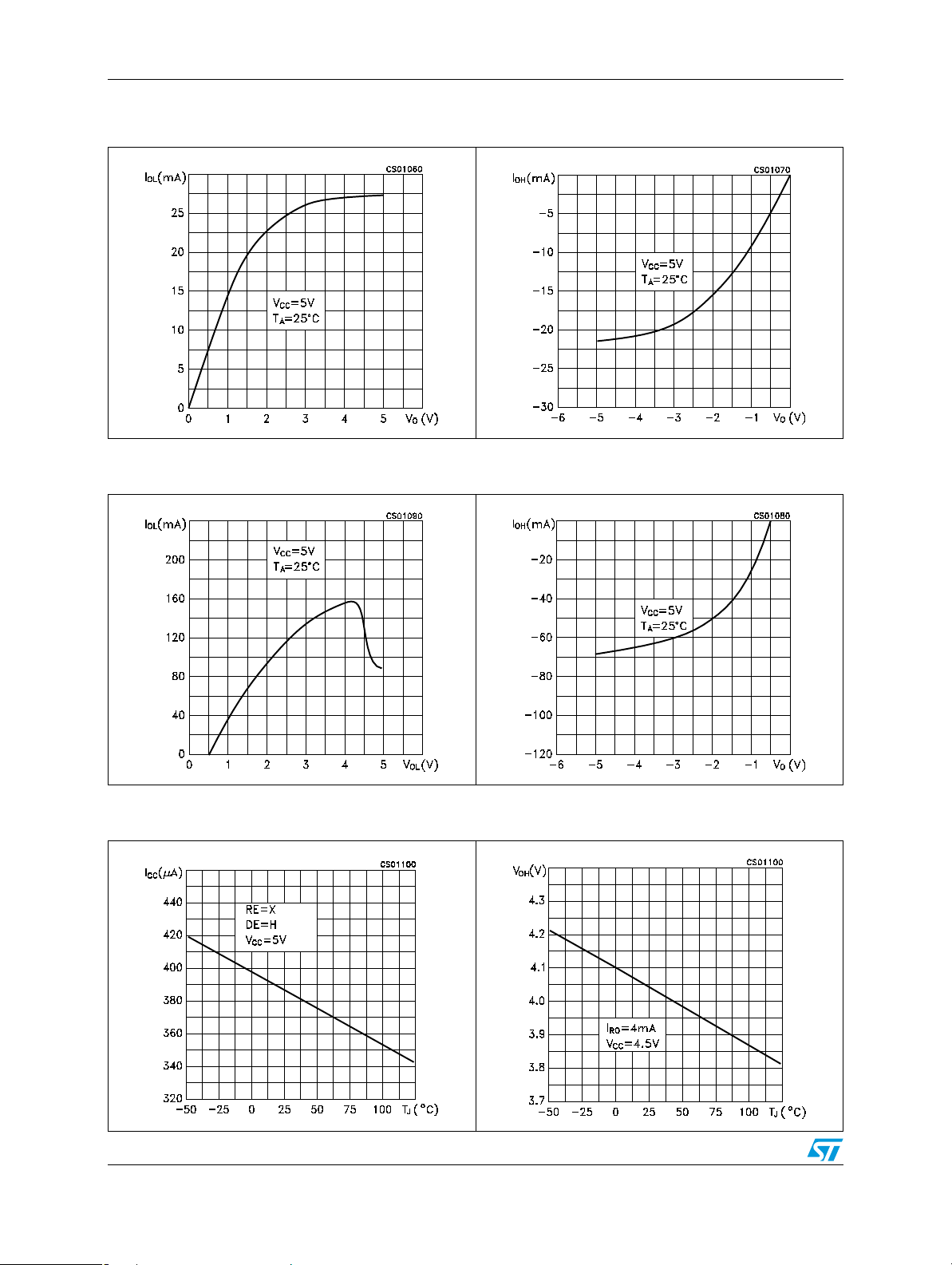
Figure 10. Receiver output current vs. output
low voltage
Figure 12. Driver output current vs. output low
voltage
Figure 11. Receiver output current vs. output
high voltage
Figure 13. Driver output current vs. output
high voltage
Figure 14. Supply current vs. temperature Figure 15. Receiver high level output voltage
12/19
vs. temperature
Page 13
ST485ERB Test circuit and typical characteristics
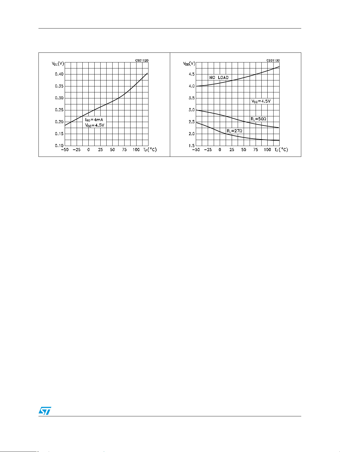
Figure 16. Receiver low level output voltage
vs. temperature
Figure 17. Differential driver output voltage vs.
temperature
13/19
Page 14

Package mechanical data ST485ERB
6 Package mechanical data
In order to meet environmental requirements, ST offers these devices in different grades of
ECOPACK
specifications, grade definitions and product status are available at: www.st.com. ECOPACK
is an ST trademark.
®
packages, depending on their level of environmental compliance. ECOPACK®
14/19
Page 15
ST485ERB Package mechanical data
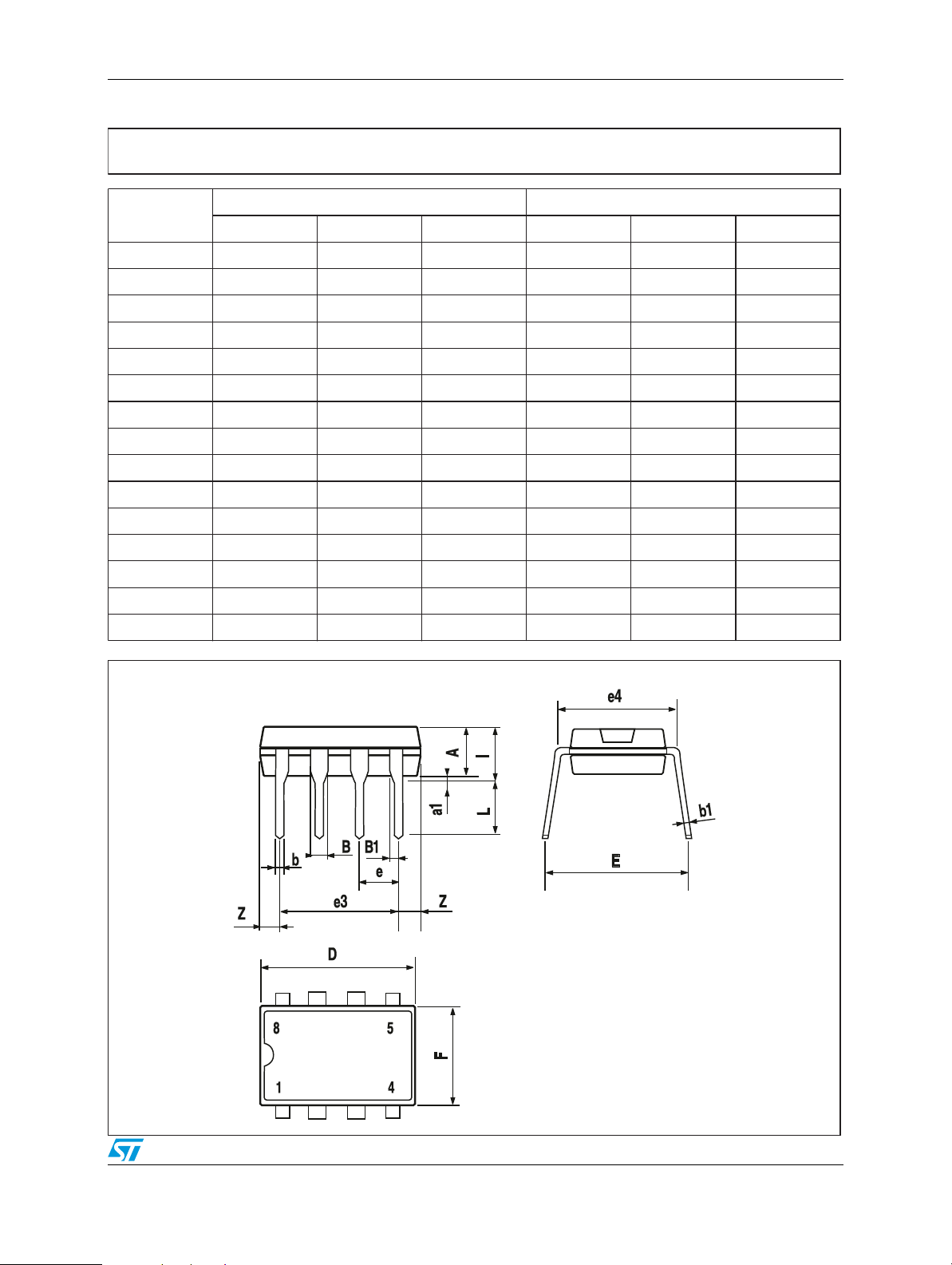
Plastic DIP-8 mechanical data
Dim.
Min. Typ. Max. Min. Typ. Max.
A 3.3 0.130
a1 0.7 0.028
B1.39 1.65 0.055 0.065
B1 0.91 1.04 0.036 0.041
b 0.5 0.020
b10.38 0.5 0.015 0.020
D 9.8 0.386
E 8.8 0.346
e 2.54 0.100
e3 7.62 0.300
e4 7.62 0.300
F 7.1 0.280
I4.8 0.189
L 3.3 0.130
Z 0.44 1.6 0.017 0.063
mm. inch.
P001F
15/19
Page 16
Package mechanical data ST485ERB
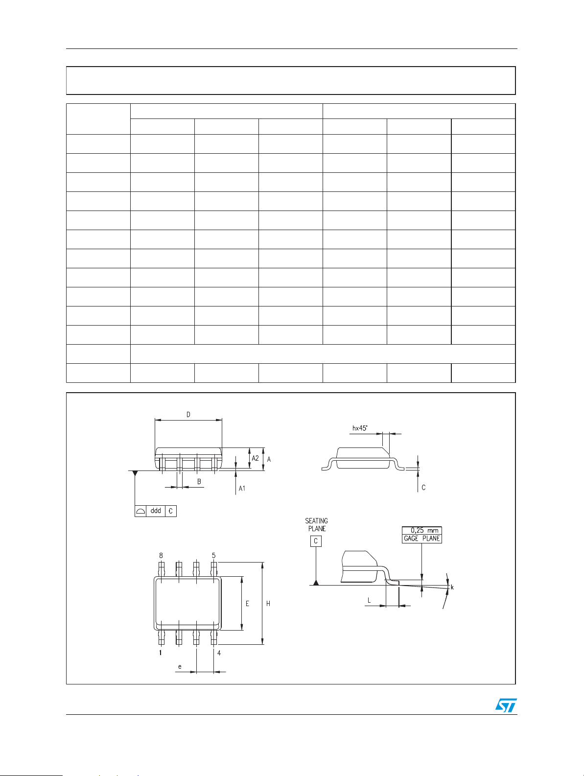
SO-8 mechanical data
Dim.
A1.35 1.75 0.053 0.069
A1 0.10 0.25 0.04 0.010
A2 1.10 1.65 0.043 0.065
B0.33 0.51 0.013 0.020
C0.19 0.25 0.007 0.010
D4.80 5.00 0.189 0.197
E 3.80 4.00 0.150 0.157
e 1.27 0.050
H5.80 6.20 0.228 0.244
h 0.25 0.50 0.010 0.020
L 0.40 1.27 0.016 0.050
k 8° (max.)
ddd 0.1 0.04
Min. Typ. Max. Min. Typ. Max.
mm. inch.
16/19
0016023/C
Page 17
ST485ERB Package mechanical data
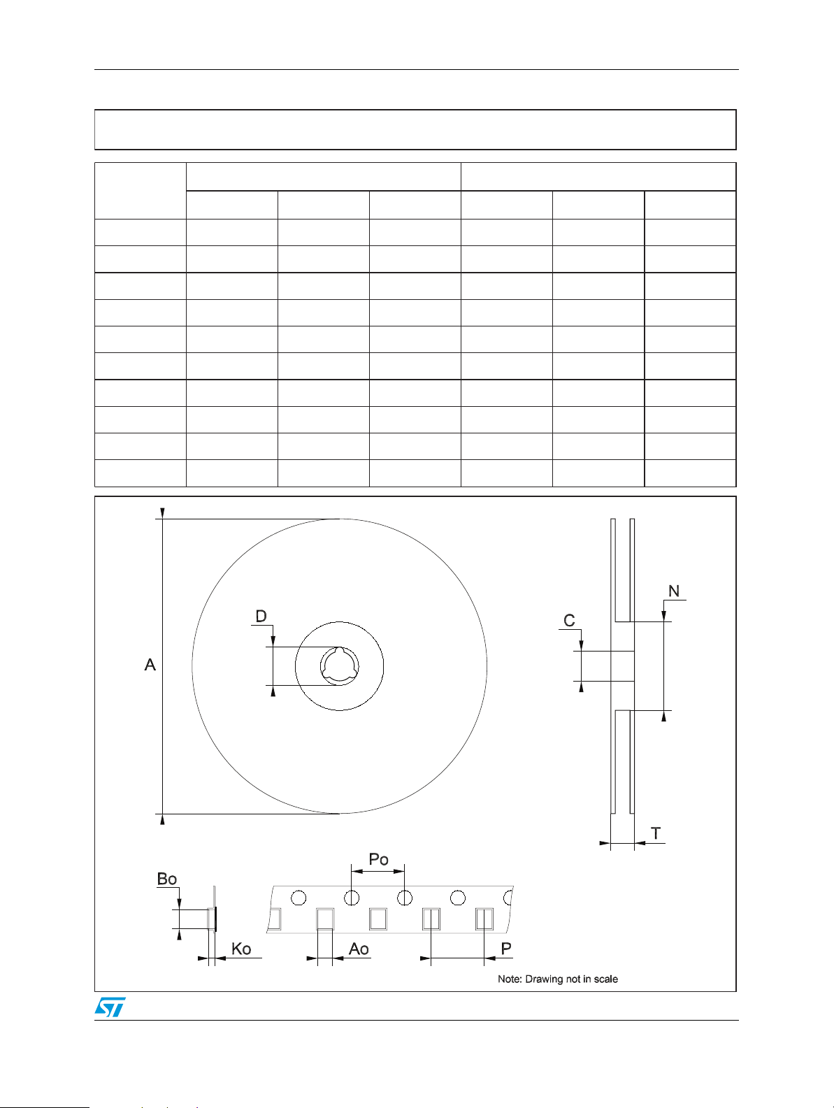
Tape & reel SO-8 mechanical data
mm. inch.
Dim.
Min. Typ. Max. Min. Typ. Max.
A 330 12.992
C 12.8 13.2 0.504 0.519
D 20.2 0.795
N60 2.362
T 22.4 0.882
Ao 8.1 8.5 0.319 0.335
Bo 5.5 5.9 0.216 0.232
Ko 2.1 2.3 0.082 0.090
Po 3.9 4.1 0.153 0.161
P7.98.1 0.311 0.319
17/19
Page 18
Revision history ST485ERB
7 Revision history
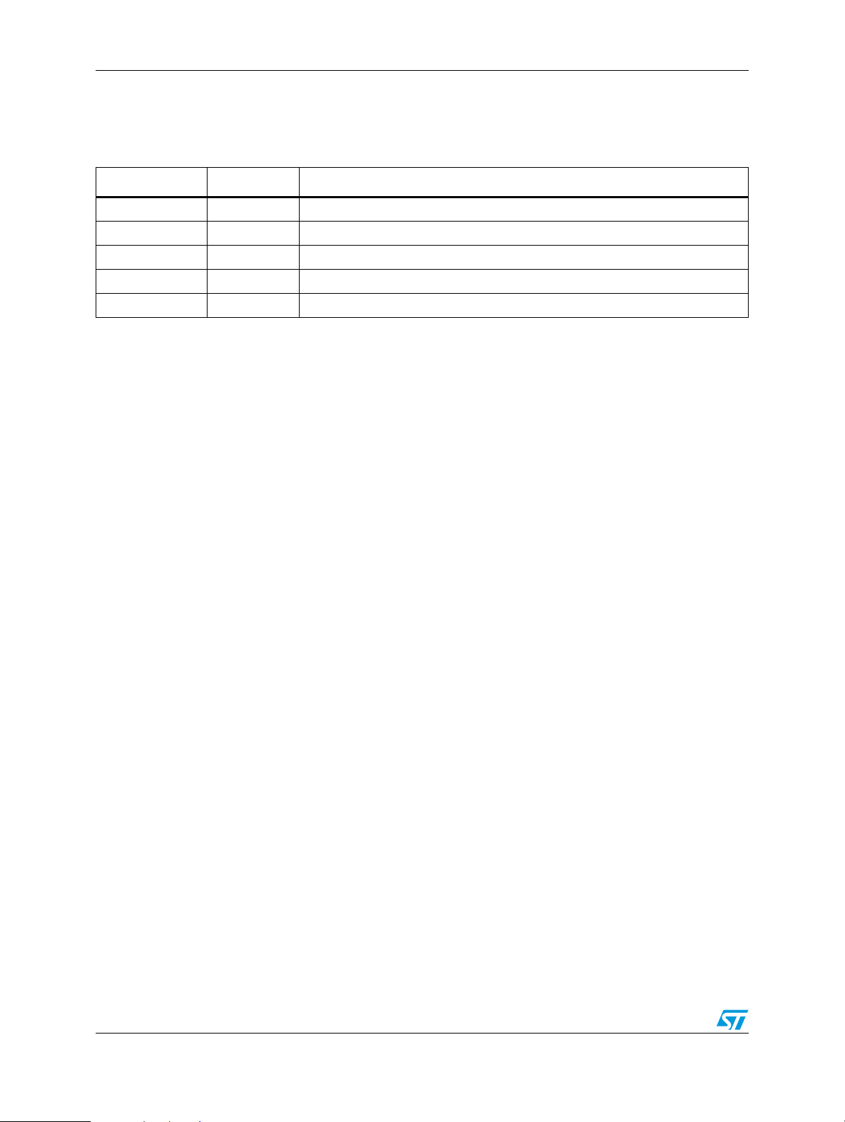
Table 10. Document revision history
Date Revision Changes
21-Mar-2006 3 Order codes has been updated and new template.
01-Aug-2006 4 Mistake in cover page description 300 mA ==> 300 µA.
25-Oct-2006 5 Order codes updated.
02-Dec-2008 6 Modified: device name Table 1 on page 1.
16-Feb-2008 7 Modified Note: on page 5.
18/19
Page 19

ST485ERB
Please Read Carefully:
Information in this document is provided solely in connection with ST products. STMicroelectronics NV and its subsidiaries (“ST”) reserve the
right to make changes, corrections, modifications or improvements, to this document, and the products and services described herein at any
time, without notice.
All ST products are sold pursuant to ST’s terms and conditions of sale.
Purchasers are solely responsible for the choice, selection and use of the ST products and services described herein, and ST assumes no
liability whatsoever relating to the choice, selection or use of the ST products and services described herein.
No license, express or implied, by estoppel or otherwise, to any intellectual property rights is granted under this document. If any part of this
document refers to any third party products or services it shall not be deemed a license grant by ST for the use of such third party products
or services, or any intellectual property contained therein or considered as a warranty covering the use in any manner whatsoever of such
third party products or services or any intellectual property contained therein.
UNLESS OTHERWISE SET FORTH IN ST’S TERMS AND CONDITIONS OF SALE ST DISCLAIMS ANY EXPRESS OR IMPLIED
WARRANTY WITH RESPECT TO THE USE AND/OR SALE OF ST PRODUCTS INCLUDING WITHOUT LIMITATION IMPLIED
WARRANTIES OF MERCHANTABILITY, FITNESS FOR A PARTICULAR PURPOSE (AND THEIR EQUIVALENTS UNDER THE LAWS
OF ANY JURISDICTION), OR INFRINGEMENT OF ANY PATENT, COPYRIGHT OR OTHER INTELLECTUAL PROPERTY RIGHT.
UNLESS EXPRESSLY APPROVED IN WRITING BY AN AUTHORIZED ST REPRESENTATIVE, ST PRODUCTS ARE NOT
RECOMMENDED, AUTHORIZED OR WARRANTED FOR USE IN MILITARY, AIR CRAFT, SPACE, LIFE SAVING, OR LIFE SUSTAINING
APPLICATIONS, NOR IN PRODUCTS OR SYSTEMS WHERE FAILURE OR MALFUNCTION MAY RESULT IN PERSONAL INJURY,
DEATH, OR SEVERE PROPERTY OR ENVIRONMENTAL DAMAGE. ST PRODUCTS WHICH ARE NOT SPECIFIED AS "AUTOMOTIVE
GRADE" MAY ONLY BE USED IN AUTOMOTIVE APPLICATIONS AT USER’S OWN RISK.
Resale of ST products with provisions different from the statements and/or technical features set forth in this document shall immediately void
any warranty granted by ST for the ST product or service described herein and shall not create or extend in any manner whatsoever, any
liability of ST.
ST and the ST logo are trademarks or registered trademarks of ST in various countries.
Information in this document supersedes and replaces all information previously supplied.
The ST logo is a registered trademark of STMicroelectronics. All other names are the property of their respective owners.
© 2009 STMicroelectronics - All rights reserved
STMicroelectronics group of companies
Australia - Belgium - Brazil - Canada - China - Czech Republic - Finland - France - Germany - Hong Kong - India - Israel - Italy - Japan -
Malaysia - Malta - Morocco - Singapore - Spain - Sweden - Switzerland - United Kingdom - United States of America
www.st.com
19/19
 Loading...