

Page 1
查询ST2L05供应商
ST2L05
VERY LOW QUIESCENT CURRENT
DUAL VOLTAGE REGULATOR
■ V
■ V
■ GUARANTEED OUTPUT1 CURRENT: 1A
■ GUARANTEED OUTPUT2 CURRENT: 1A
■ ± 2% OUTPUT TOLERANCE (AT 25°C)
■ ± 3% OUTPUT TOLERANCE OVER TEMP.
■ TYPICAL DROPOUT 1.1V (I
■ INTERNAL POWER AND T HERMAL LIMIT
■ STABLE WITH LOW ESR OUTPUT
= 1.5, 1.8, 2.5, 2.8, 3.0, 3.3V FIXED
O1
= 1.5, 1.8, 2.5, 2.8, 3.0, 3.3V FIXED OR
O2
ADJUSTABLE FROM 1.25 TO V
I-VDROP
O1=IO2
=1A)
CAPACITOR
■ OPERATING TEMPERATURE R ANGE:
0°C TO 125°C
■ VERY LOW Q UIESCENT CURRENT: 7mA
MAX OVER TEMP.
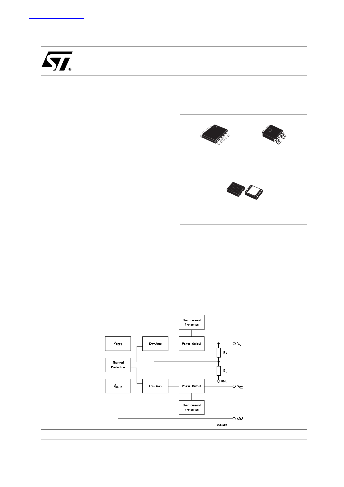
■ AVAILABLEIN PPAK, SPAK AND IN DFN
5x6mm PACKAGE
DESCRIPTION
Specifically designed for data storage
applications, this device integrates two voltage
regulators, each one able to supply 1A and it is
assembled in PPAK, in SPAK and in a new 8-PIN
surface mounting package named DFN 5x 6mm at
8 pins. The first regulator block supplies 1.5V,
1.8V, 2.5V, 2.8V, 3.0V, 3.3V depending on the
SPAK-5L
DFN
PPAK
chosen version. The s ec ond one m ay be fixed to
the same values or adjustable from 1.25V to V
V
that could power several kind of different
DROP
I
micro-controllers. Both outputs are c urrent limited
and over temperature p rotected. It is worth
underlining the very good thermal performance of
the pack ages SPAK and DFN with only 2°C/W of
Thermal Resistance Junction to Case.
Applications are HARD DISK, CD/DVD-ROM, CD/
DVD-R/RW, C OMBO (DVD-ROM+CD-R/RW).
-
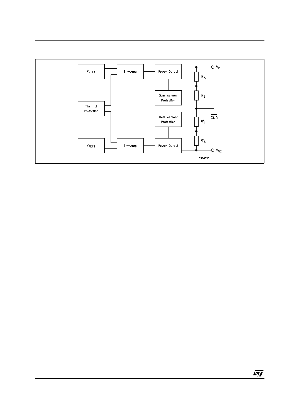
BLOCK DIAGRAM OF FIXED/ADJ VERSION
1/24October 2003
Page 2
ST2L05
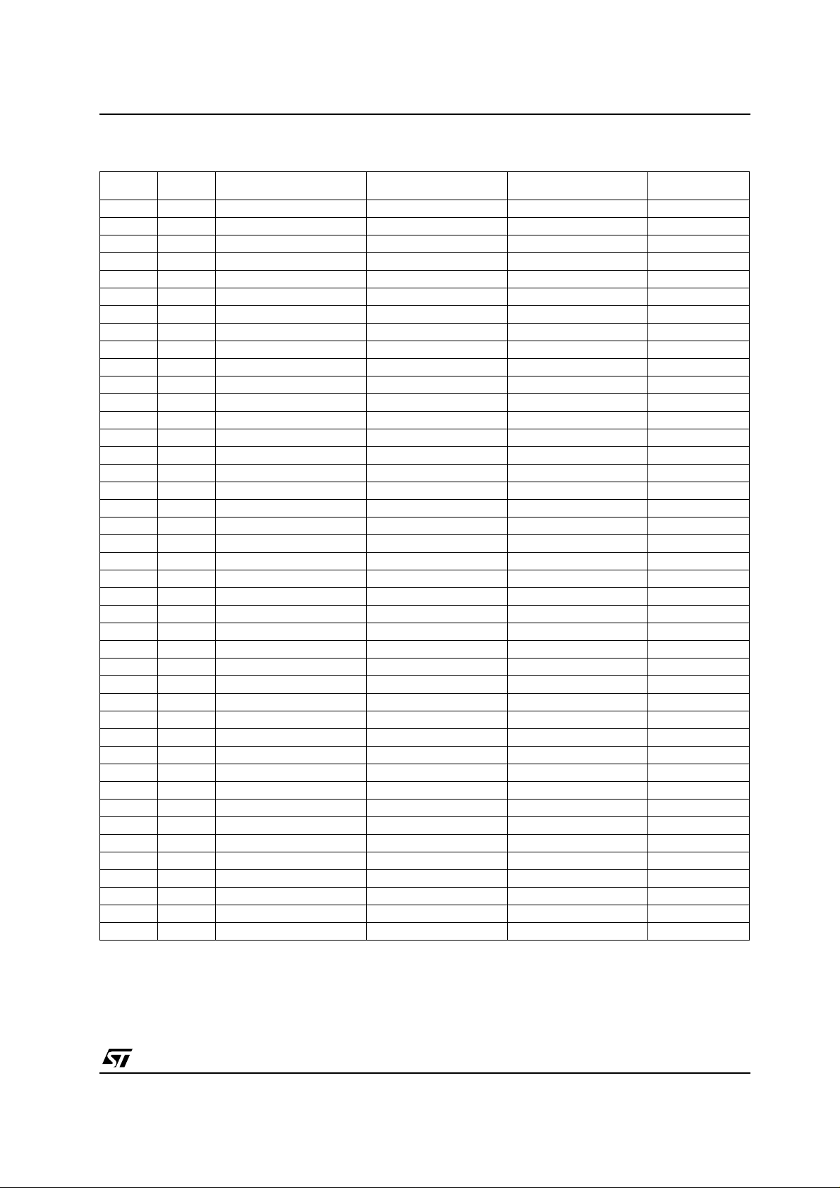
BLOCK DIAGRAM OF FIXED/FIXEDVERSION
2/24
Page 3
ORDERING CODES
ST2L05
V
O1
V
O2
SPAK PPAK
DFN SHIPMENT
1.5 V 1.5 V ST2L05R1515K5 (*) ST2L05R1515PT (*) ST2L05R1515PS (*) Tape & Reel
1.5 V 1.8 V ST2L05R1518K5 (*) ST2L05R1518PT (*) ST2L05R1518PS (*) Tape & Reel
1.5 V 2.5 V ST2L05R1525K5 (*) ST2L05R1525PT (*) ST2L05R1525PS (*) Tape & Reel
1.5 V 2.8 V ST2L05R1528K5 (*) ST2L05R1528PT (*) ST2L05R1528PS (*) Tape & Reel
1.5 V 3.0 V ST2L05R1530K5 (*) ST2L05R1530PT (*) ST2L05R1530PS (*) Tape & Reel
1.5 V 3.3 V ST2L05R1533K5 (*) ST2L05R1533PT (*) ST2L05R1533PS (*) Tape & Reel
1.5 V ADJ ST2L05R1500K5 (*) ST2L05R1500PT ST2L05R1500PS (*) Tape & Reel
1.8 V 1.5 V ST2L05R1815K5 (*) ST2L05R1815PT (*) ST2L05R1815PS (*) Tape & Reel
1.8 V 1.8 V ST2L05R1818K5 (*) ST2L05R1818PT (*) ST2L05R1818PS (*) Tape & Reel
1.8 V 2.5 V ST2L05R1825K5 (*) ST2L05R1825PT ST2L05R1825PS (*) Tape & Reel
1.8 V 2.8 V ST2L05R1828K5 (*) ST2L05R1828PT (*) ST2L05R1828PS (*) Tape & Reel
1.8 V 3.0 V ST2L05R1830K5 (*) ST2L05R1830PT (*) ST2L05R1830PS (*) Tape & Reel
1.8 V 3.3 V ST2L05R1833K5 (*) ST2L05R1833PT (*) ST2L05R1833PS (*) Tape & Reel
1.8 V ADJ ST2L05R1800K5 (*) ST2L05R1800PT ST2L05R1800PS (*) Tape & Reel
2.5 V 1.5 V ST2L05R2515K5 (*) ST2L05R2515PT (*) ST2L05R2515PS (*) Tape & Reel
2.5 V 1.8 V ST2L05R2518K5 (*) ST2L05R2518PT (*) ST2L05R2518PS (*) Tape & Reel
2.5 V 2.5 V ST2L05R2525K5 (*) ST2L05R2525PT (*) ST2L05R2525PS (*) Tape & Reel
2.5 V 2.8 V ST2L05R2528K5 (*) ST2L05R2528PT (*) ST2L05R2528PS (*) Tape & Reel
2.5 V 3.0 V ST2L05R2530K5 (*) ST2L05R2530PT (*) ST2L05R2530PS (*) Tape & Reel
2.5 V 3.3 V ST2L05R2533K5 (*) ST2L05R2533PT (*) ST2L05R2533PS (*) Tape & Reel
2.5 V ADJ ST2L05R2500K5 (*) ST2L05R2500PT ST2L05R2500PS (*) Tape & Reel
2.8 V 1.5 V ST2L05R2815K5 (*) ST2L05R2815PT (*) ST2L05R2815PS (*) Tape & Reel
2.8 V 1.8 V ST2L05R2818K5 (*) ST2L05R2818PT (*) ST2L05R2818PS (*) Tape & Reel
2.8 V 2.5 V ST2L05R2825K5 (*) ST2L05R2825PT (*) ST2L05R2825PS (*) Tape & Reel
2.8 V 2.8 V ST2L05R2828K5 (*) ST2L05R2828PT (*) ST2L05R2828PS (*) Tape & Reel
2.8 V 3.0 V ST2L05R2830K5 (*) ST2L05R2830PT (*) ST2L05R2830PS (*) Tape & Reel
2.8 V 3.3 V ST2L05R2833K5 (*) ST2L05R2833PT (*) ST2L05R2833PS (*) Tape & Reel
2.8 V ADJ ST2L05R2800K5 (*) ST2L05R2800PT (*) ST2L05R2800PS (*) Tape & Reel
3.0 V 1.5 V ST2L05R3015K5 (*) ST2L05R3015PT (*) ST2L05R3015PS (*) Tape & Reel
3.0 V 1.8 V ST2L05R3018K5 (*) ST2L05R3018PT (*) ST2L05R3018PS (*) Tape & Reel
3.0 V 2.5 V ST2L05R3025K5 (*) ST2L05R3025PT (*) ST2L05R3025PS (*) Tape & Reel
3.0 V 2.8 V ST2L05R3028K5 (*) ST2L05R3028PT (*) ST2L05R3028PS (*) Tape & Reel
3.0 V 3.0 V ST2L05R3030K5 (*) ST2L05R3030PT (*) ST2L05R3030PS (*) Tape & Reel
3.0 V 3.3 V ST2L05R3033K5 (*) ST2L05R3033PT (*) ST2L05R3033PS (*) Tape & Reel
3.0 V ADJ ST2L05R3000K5 (*) ST2L05R3000PT (*) ST2L05R3000PS (*) Tape & Reel
3.3 V 1.5 V ST2L05R3315K5 (*) ST2L05R3315PT (*) ST2L05R3315PS (*) Tape & Reel
3.3 V 1.8 V ST2L05R3318K5 (*) ST2L05R3318PT ST2L05R3318PS (*) Tape & Reel
3.3 V 2.5 V ST2L05R3325K5 (*) ST2L05R3325PT ST2L05R3325PS Tape & Reel
3.3 V 2.8 V ST2L05R3328K5 (*) ST2L05R3328PT (*) ST2L05R3328PS (*) Tape & Reel
3.3 V 3.0 V ST2L05R3330K5 (*) ST2L05R3330PT (*) ST2L05R3330PS (*) Tape & Reel
3.3 V 3.3 V ST2L05R3333K5 (*) ST2L05R3333PT (*) ST2L05R3333PS (*) Tape & Reel
3.3 V ADJ ST2L05R3300K5 ST2L05R3300PT ST2L05R3300PS Tape & Reel
(*) Available on request.
(1) For Tube Shipment, change "R" with "-" in the relevant ordering code, DFN is available only in Tape & Reel.
(1)
3/24
Page 4
ST2L05
ABSOLUTE MAXIMUM RATINGS
Symbol Parameter Value Unit
V
P
I
OSH
T
T
T
LEAD
(*) Storage temperatures > 125°C are only acceptable if the Dual Regulator is soldered to a PCBA.
Absolute Maximum Ratings are those beyond which damage to the device may occur. Functional operation under these condition is not implied.
RECOMMENDED OPERATING CONDITIONS
Symbol Parameter Value Unit
V
∆V
t
RISE
t
FALL
Operating Input Voltage
I
Power Dissipation
D
Short Circuit Output Current - 3.3 V and adjustable output
Operating Junction Temperature Range
op
Storage Temperature Range
stg
(*)
Lead Temperature (Soldering) 10 Sec.
Input Voltage
I
Input Voltage Ripple
I
Input Voltage Rise Time (from 10% to 90%)
Input Voltage Fall Time (from 10% to 90%)
10 V
Internally Limited
Internally Limited
0 to 150 °C
-65 to 150 °C
260 °C
4.5 to 7 V
±0.15 V
≥ 1 µsec
≥ 1 µsec
THERMAL DATA
Symbol Parameter SPAK DFN PPAK Unit
R
thj-case
R
thj-amb
Thermal Resistance Junction-case
Thermal Resistance Junction-ambient
228°C/W
26 36 100 °C/W
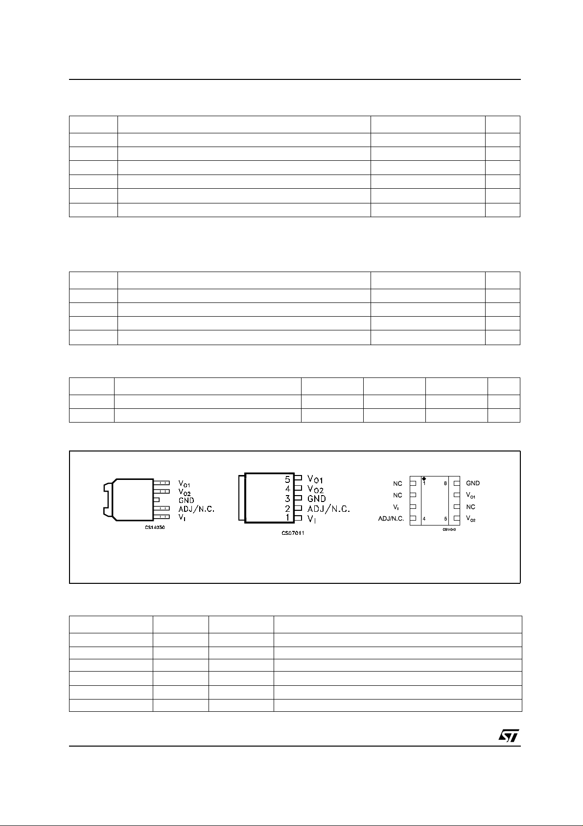
CONNECTION DIAGRAM (top view for PPAK and SPAK, top through view for DFN8)
DFN8PPAK SPAK
PIN DESCRIPTION
PPAK/SPAK DFN Symbol Name and Function
13V
I
2 4 ADJ/N.C. Resistor divider connection/Not Connected
3 8 GND Ground
45V
57V
O2
O1
1, 2, 6 NC Not Connected
Bypass with a 4.7µF capacitor to GND
Adjustable output voltage: bypass with a 4.7µF capacitor to GND
Fixed output voltage: bypass with a 4.7µF capacitor to GND
4/24
Page 5
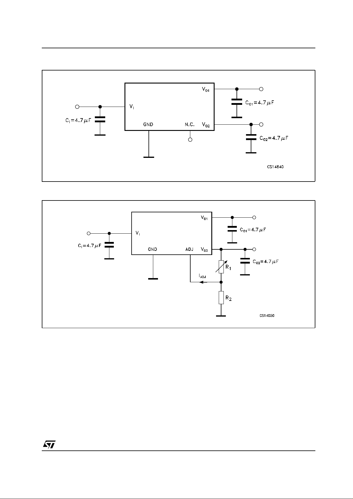
APPLICATION CIRCUIT OF FIXED/FIXED VERSION
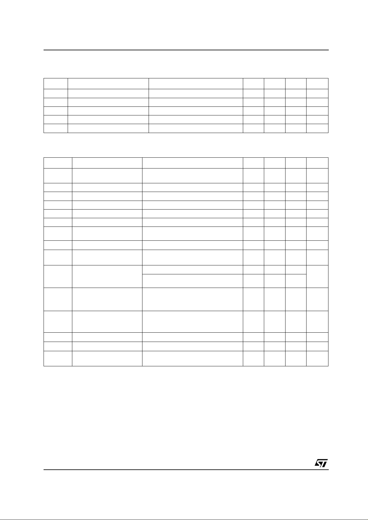
APPLICATION CIRCUIT OF FIXED/ADJ VERSION
ST2L05
NOTE: The regulator is designed to be stable with either tantalum or ceramic capacitors on the input and outputs. The expected values of
the input and output X7R ceramic capacitors are from 4.7µF to 22µF with 4.7µF typical. The input capacitor must be connected within 0.5
inches of theVIterminal. The output capacitors must also be connected within 0.5 inches of output pins VO1andVO2. There is no upper limit
to the size of the in put capacitor (for more details see the Application Hints section).
NOTE: In the Fixed/ADJ version, the adjustable output voltage V
adjustable output voltage V
VO2ADJ (pin2). The voltage divider resistors are: R1connected to VO2and VO2ADJ and R2connected to VO2ADJ and GND. VO2is determined by V
V
O2=VREF
REF,R1,R2
(1+R1/R2)+I
is set by a resistor divider connected between VO2(pin4) and Ground (pin3) with its centre tap connected to
O2
, and I
as follows (for more detailssee the Application Hintssection):
ADJ
ADJR1
is designed to support output voltages from 1.25V to VI-V
O2
DROP
.The
5/24
Page 6
ST2L05
OUTPUT1 AND OUT PUT2 DUAL SPECIFICATION (IO=10mAto1A,TJ= 0 to 125°C, VI=4.5Vto7V,
C
=4.7µF,CO1=CO2=4.7µF, otherwise specified)
I
Symbol Parameter Test Conditions Min. Typ. Max. Unit
I
I
T
DT
Quiescent Current (Fixed/ADJ) VI≤ 7V I
GND
Quiescent Current (Fixed/Fixed) VI≤ 7V I
GND
Total Current Limit IO1+I
I
ST
Thermal Shutdown 175 °C
SHDN
Thermal Shutdown Hysteresis 5 °C
SHDN
O2
= 5mA to 1A 5 mA
OUT1,2
= 5mA to 1A 7 mA
OUT1,2
2A
ELECTRICAL CHARACTERISTICS OF FIXED OUTPUT 1.5V (I
V
=4.5Vto7V,CI= 4.7µF, CO1=CO2=4.7µF, otherwise specified)
I
=10mAto1A,TJ= 0 to 125°C,
O
Symbol Parameter Test Conditions Min. Typ. Max. Unit
V
Output Voltage 1.5V IO= 5mA to 1A, VI= 4.75 to 5.25V
O
1.47 1.5 1.53 V
T = 25°C
V
∆V
∆V
V
I
OMIN
e
SVR Supply Voltage
∆V
O
∆VO1/∆VITransient Response
∆V
O
T
Output Voltage 1.5V IO= 5mA to 1A, VI= 4.75 to 5.25V 1.455 1.5 1.545 V
O
Line Regulation VI= 4.75 to 5.25V, IO= 5mA to 1A 15 mV
O
Load Regulation VI= 4.75V, IO= 10mA to 1A 12 mV
O
Dropout Voltage ∆VO= -1% IO= 1A 1.3 V
D
Current Limit VI= 5.5V 1 A
I
S
Min Output Current for
regulation
N
RMS Output Noise
(1)(4)
T = 25°C 0.003 %
VI=5V 60 dB
Rejection
/∆IOTransient Response
Change of V
load change
(2)(4)
(3)(4)
with step
O
VI=5V, IO= 1mA to 1A, tr≥ 1µs
V
=5V, IO=1Ato1mA, tf≥ 1µs
I
0 to 5V step input, IO= 1mA to 1A,
Change of V
application of V
/∆IOTransient Response Short
OUT1
(3)(4)
I
with
t
≥ 1µs
r
VI=5V, IO= short to IO= 10mA
Circuit Removal
Response
R
Thermal Regulation
S
Temperature Stability
S
Long Term Stability
(3)(4)
(4)
(4)
(4)
IO= 1A, t
= 30ms 0.1 %/W
PULSE
0.5 %
= 125°C 0.3 %
T
J
0mA
(5)
10
(5)
10
(5)
10
(5)
20
(1000Hrs)
NOTE 1: Bandwidth of 10 Hz to 10KHz.
NOTE 2: 120Hz input ripple.
NOTE 3: C
NOTE 4: Guaranteed by design, not tested in production.
NOTE 5: % undershoot or overshoot of V
= 20µF, C1and CO2= 10µF. CI,CO1and CO2are all X7R ceramic capacitors.
I
.
O
%
%
%
6/24
Page 7
ST2L05
ELECTRICAL CHARACTERISTICS OF FIXED OUTPUT 1.8V (IO=10mAto1A,TJ= 0 to 125°C,
V
=4.5Vto7V,CI= 4.7µF, CO1=CO2=4.7µF, otherwise specified)
I
Symbol Parameter Test Conditions Min. Typ. Max. Unit
V
V
∆V
∆V
V
I
OMIN
e
SVR Supply Voltage
∆V
O
∆VO1/∆VITransient Response
∆V
O
T
NOTE 1: Bandwidth of 10 Hz to 10KHz.
NOTE 2: 120Hz input ripple.
NOTE 3: C
NOTE 4: Guaranteed by design, not tested in production.
NOTE 5: % undershoot or overshoot of V
Output Voltage 1.8V IO= 5mA to 1A, VI= 4.75 to 5.25V
O
1.764 1.8 1.836 V
T = 25°C
Output Voltage 1.8V IO= 5mA to 1A, VI= 4.75 to 5.25V 1.746 1.8 1.854 V
O
Line Regulation VI= 4.75 to 5.25V, IO= 5mA to 1A 15 mV
O
Load Regulation VI= 4.75V, IO= 10mA to 1A 12 mV
O
Dropout Voltage ∆VO= -1% IO= 1A 1.3 V
D
Current Limit VI= 5.5V 1 A
I
S
Min Output Current for
regulation
NRMS Output Noise
(1)(4)
T = 25°C 0.003 %
VI=5V 60 dB
Rejection
/∆IOTransient Response
Change of V
load change
(2)(4)
(3)(4)
with step
O
VI=5V, IO= 1mA to 1A, tr≥ 1µs
V
=5V, IO=1Ato1mA, tf≥ 1µs
I
0 to 5V step input, IO= 1mA to 1A,
Change of V
application of V
/∆IOTransient Response Short
OUT1
(3)(4)
I
with
t
≥ 1µs
r
VI=5V, IO= short to IO= 10mA
Circuit Removal
Response
R Thermal Regulation
S
Temperature Stability
S
Long Term Stability
(3)(4)
(4)
(4)
(4)
IO= 1A, t
= 30ms 0.1 %/W
PULSE
0.5 %
T
= 125°C 0.3 %
J
(1000Hrs)
= 20µF, C1and CO2= 10µF. CI,CO1and CO2are all X7R ceramic capacitors.
I
.
O
0mA
(5)
10
(5)
10
(5)
10
(5)
20
%
%
%
7/24
Page 8
ST2L05
ELECTRICAL CHARACTERISTICS OF FIXED OUTPUT 2.5V (IO=10mAto1A,TJ= 0 to 125°C,
V
=4.5Vto7V,CI= 4.7µF, CO1=CO2=4.7µF, otherwise specified)
I
Symbol Parameter Test Conditions Min. Typ. Max. Unit
V
V
∆V
∆V
V
I
OMIN
e
SVR Supply Voltage
∆V
O
∆VO1/∆VITransient Response
∆V
O
T
NOTE 1: Bandwidth of 10 Hz to 10KHz.
NOTE 2: 120Hz input ripple.
NOTE 3: C
NOTE 4: Guaranteed by design, not tested in production.
NOTE 5: % undershoot or overshoot of V
Output Voltage 2.5V IO= 5mA to 1A, VI= 4.75 to 5.25V
O
2.45 2.5 2.55 V
T = 25°C
Output Voltage 2.5V IO= 5mA to 1A, VI= 4.75 to 5.25V 2.425 2.5 2.575 V
O
Line Regulation VI= 4.75 to 5.25V, IO= 5mA to 1A 15 mV
O
Load Regulation VI= 4.75V, IO= 10mA to 1A 12 mV
O
Dropout Voltage ∆VO= -1% IO= 1A 1.3 V
D
Current Limit VI= 5.5V 1 A
I
S
Min Output Current for
regulation
NRMS Output Noise
(1)(4)
T = 25°C 0.003 %
VI=5V 60 dB
Rejection
/∆IOTransient Response
Change of V
load change
(2)(4)
(3)(4)
with step
O
VI=5V, IO= 1mA to 1A, tr≥ 1µs
V
=5V, IO=1Ato1mA, tf≥ 1µs
I
0 to 5V step input, IO= 1mA to 1A,
Change of V
application of V
/∆IOTransient Response Short
OUT1
(3)(4)
I
with
t
≥ 1µs
r
VI=5V, IO= short to IO= 10mA
Circuit Removal
Response
R
Thermal Regulation
S
Temperature Stability
S
Long Term Stability
(3)(4)
(4)
(4)
(4)
IO= 1A, t
= 30ms 0.1 %/W
PULSE
0.5 %
T
= 125°C 0.3 %
J
(1000Hrs)
= 20µF, C1and CO2= 10µF. CI,CO1and CO2are all X7R ceramic capacitors.
I
.
O
0mA
(5)
10
(5)
10
(5)
10
(5)
20
%
%
%
8/24
Page 9

ST2L05
ELECTRICAL CHARACTERISTICS OF FIXED OUTPUT 2.8V (IO=10mAto1A,TJ= 0 to 125°C,
V
=4.5Vto7V,CI= 4.7µF, CO1=CO2=4.7µF, otherwise specified)
I
Symbol Parameter Test Conditions Min. Typ. Max. Unit
V
V
∆V
∆V
V
I
OMIN
e
SVR Supply Voltage
∆V
O
∆VO1/∆VITransient Response
∆V
O
T
NOTE 1: Bandwidth of 10 Hz to 10KHz.
NOTE 2: 120Hz input ripple.
NOTE 3: C
NOTE 4: Guaranteed by design, not tested in production.
NOTE 5: % undershoot or overshoot of V
Output Voltage 2.8V IO= 5mA to 1A, VI= 4.75 to 5.25V
O
2.744 2.8 2.856 V
T = 25°C
Output Voltage 2.8V IO= 5mA to 1A, VI= 4.75 to 5.25V 2.716 2.8 2.884 V
O
Line Regulation VI= 4.75 to 5.25V, IO= 5mA to 1A 15 mV
O
Load Regulation VI= 4.75V, IO= 10mA to 1A 12 mV
O
Dropout Voltage ∆VO= -1% IO= 1A 1.3 V
D
Current Limit VI= 5.5V 1 A
I
S
Min Output Current for
regulation
NRMS Output Noise
(1)(4)
T = 25°C 0.003 %
VI=5V 60 dB
Rejection
/∆IOTransient Response
Change of V
load change
(2)(4)
(3)(4)
with step
O
VI=5V, IO= 1mA to 1A, tr≥ 1µs
V
=5V, IO=1Ato1mA, tf≥ 1µs
I
0 to 5V step input, IO= 1mA to 1A,
Change of V
application of V
/∆IOTransient Response Short
OUT1
(3)(4)
I
with
t
≥ 1µs
r
VI=5V, IO= short to IO= 10mA
Circuit Removal
Response
R Thermal Regulation
S
Temperature Stability
S
Long Term Stability
(3)(4)
(4)
(4)
(4)
IO= 1A, t
= 30ms 0.1 %/W
PULSE
0.5 %
T
= 125°C 0.3 %
J
(1000Hrs)
= 20µF, C1and CO2= 10µF. CI,CO1and CO2are all X7R ceramic capacitors.
I
.
O
0mA
(5)
10
(5)
10
(5)
10
(5)
20
%
%
%
9/24
Page 10

ST2L05
ELECTRICAL CHARACTERISTICS OF FIXED OUTPUT 3.0V (IO=10mAto1A,TJ= 0 to 125°C,
V
=4.5Vto7V,CI= 4.7µF, CO1=CO2=4.7µF, otherwise specified)
I
Symbol Parameter Test Conditions Min. Typ. Max. Unit
V
V
∆V
∆V
V
I
OMIN
e
SVR Supply Voltage
∆V
O
∆VO1/∆VITransient Response
∆V
O
T
NOTE 1: Bandwidth of 10 Hz to 10KHz.
NOTE 2: 120Hz input ripple.
NOTE 3: C
NOTE 4: Guaranteed by design, not tested in production.
NOTE 5: % undershoot or overshoot of V
Output Voltage 3.0V IO= 5mA to 1A, VI= 4.75 to 5.25V
O
2.94 3.0 3.06 V
T = 25°C
Output Voltage 3.0V IO= 5mA to 1A, VI= 4.75 to 5.25V 2.91 3.0 3.09 V
O
Line Regulation VI= 4.75 to 5.25V, IO= 5mA to 1A 15 mV
O
Load Regulation VI= 4.75V, IO= 10mA to 1A 12 mV
O
Dropout Voltage ∆VO= -1% IO= 1A 1.3 V
D
Current Limit VI= 5.5V 1 A
I
S
Min Output Current for
regulation
NRMS Output Noise
(1)(4)
T = 25°C 0.003 %
VI=5V 60 dB
Rejection
/∆IOTransient Response
Change of V
load change
(2)(4)
(3)(4)
with step
O
VI=5V, IO= 1mA to 1A, tr≥ 1µs
V
=5V, IO=1Ato1mA, tf≥ 1µs
I
0 to 5V step input, IO= 1mA to 1A,
Change of V
application of V
/∆IOTransient Response Short
OUT1
(3)(4)
I
with
t
≥ 1µs
r
VI=5V, IO= short to IO= 10mA
Circuit Removal
Response
R Thermal Regulation
S
Temperature Stability
S
Long Term Stability
(3)(4)
(4)
(4)
(4)
IO= 1A, t
= 30ms 0.1 %/W
PULSE
0.5 %
T
= 125°C 0.3 %
J
(1000Hrs)
= 20µF, C1and CO2= 10µF. CI,CO1and CO2are all X7R ceramic capacitors.
I
.
O
0mA
(5)
10
(5)
10
(5)
10
(5)
20
%
%
%
10/24
Page 11

ST2L05
ELECTRICAL CHARACTERISTICS OF FIXED OUTPUT 3.3V (IO=10mAto1A,TJ= 0 to 125°C,
V
=4.5Vto7V,CI= 4.7µF, CO1=CO2=4.7µF, otherwise specified)
I
Symbol Parameter Test Conditions Min. Typ. Max. Unit
V
V
∆V
∆V
V
I
OMIN
e
SVR Supply Voltage
∆V
O
∆VO1/∆VITransient Response
∆V
O
T
NOTE 1: Bandwidth of 10 Hz to 10KHz.
NOTE 2: 120Hz input ripple.
NOTE 3: C
NOTE 4: Guaranteed by design, not tested in production.
NOTE 5: % undershoot or overshoot of V
Output Voltage 3.3V IO= 5mA to 1A, VI= 4.75 to 5.25V
O
3.234 3.3 3.366 V
T = 25°C
Output Voltage 3.3V IO= 5mA to 1A, VI= 4.75 to 5.25V 3.2 3.3 3.4 V
O
Line Regulation VI= 4.75 to 5.25V, IO= 5mA to 1A 15 mV
O
Load Regulation VI= 4.75V, IO= 10mA to 1A 12 mV
O
Dropout Voltage ∆VO= -1% IO= 1A 1.3 V
D
Current Limit VI= 5.5V 1 A
I
S
Min Output Current for
regulation
NRMS Output Noise
(1)(4)
T = 25°C 0.003 %
VI=5V 60 dB
Rejection
/∆IOTransient Response
Change of V
load change
(2)(4)
(3)(4)
with step
O
VI=5V, IO= 1mA to 1A, tr≥ 1µs
V
=5V, IO=1Ato1mA, tf≥ 1µs
I
0 to 5V step input, IO= 1mA to 1A,
Change of V
application of V
/∆IOTransient Response Short
OUT1
(3)(4)
I
with
t
≥ 1µs
r
VI=5V, IO= short to IO= 10mA
Circuit Removal
Response
R Thermal Regulation
S
Temperature Stability
S
Long Term Stability
(3)(4)
(4)
(4)
(4)
IO= 1A, t
= 30ms 0.1 %/W
PULSE
0.5 %
T
= 125°C 0.3 %
J
(1000Hrs)
= 20µF, C1and CO2= 10µF. CI,CO1and CO2are all X7R ceramic capacitors.
I
.
O
0mA
(5)
10
(5)
10
(5)
10
(5)
20
%
%
%
11/24
Page 12

ST2L05
ELECTRICAL CHARACTERISTICS O F ADJUSTABLE OUTPUT (IO= 10mA to 1A, TJ= 0 to 125°C,
V
=4.5Vto7V,CI= 4.7µF, CO1=CO2=4.7µF, otherwise specified)
I
Symbol Parameter Test Conditions Min. Typ. Max. Unit
V
V
∆V
∆V
V
I
ADJ
I
∆ADJ
I
OMIN
e
SVR Supply Voltage
∆V
O2
∆VO2/∆VITransient Response
∆V
O2
T
NOTE 1: Bandwidth of 10 Hz to 10KHz.
NOTE 2: 120Hz input ripple.
NOTE 3: C
NOTE 4: Guaranteed by design, not tested in production.
NOTE 5: % undershoot or overshoot of V
Reference Voltage IO= 5mA to 1A, VI= 4.75 to 5.25V,
O
1.225 1.25 1.275 V
T = 25°C
Reference Voltage IO= 5mA to 1A, VI= 4.75 to 5.25V 1.212 1.25 1.287 V
O
Line Regulation 2 VI= 4.75 to 5.25V, IO= 5mA to 1A 0.35 %
O2
Load Regulation 2 VI= 4.75V, IO= 10mA to 1A 0.4 %
O2
Dropout Voltage ∆VO= -1% IO= 1A 1.3 V
D
Current Limit VI= 5.5V 1 A
I
S
Adjustable Current (sinking) 1 µA
Adjustable Current Change IO= 10mA to 1A 200 nA
Min Output Current for
regulation
N
RMS Output Noise
(1)(4)
T = 25°C 0.003 %
VI=5V 60 dB
Rejection
/∆IO2Transient Response
Change of V
load change
(2)(4)
(3)(4)
with step
O1
VI=5V, IO= 1mA to 1A, tr≥ 1µs
V
=5V, IO=1Ato1mA, tf≥ 1µs
I
0 to 5V step input, IO= 1mA to 1A,
Change of V
application of V
/∆IO2Transient Response Short
OUT1
(3)(4)
I
with
t
≥ 1µs
r
VI=5V, IO= short to IO= 10mA
Circuit Removal
Response
R
Thermal Regulation
S
Temperature Stability
S
Long Term Stability
(3)(4)
(4)
(4)
(4)
IO= 1A, t
= 30ms 0.1 %/W
PULSE
0.5 %
T
= 125°C 0.3 %
J
(1000Hrs)
= 20µF, C1and CO2= 10µF. CI,CO1and CO2are all X7R ceramic capacitors.
I
.
O
2mA
10
10
10
20
(5)
(5)
(5)
(5)
%
%
%
APPLICATION HINTS
EXTERNAL CAPACITORS
Like any low-dropout regulator, the ST2L05 requires external capacitors for stability. We suggest
soldering both capacitors as close as possible to the relative pins (1, 4 and 5).
INPUT CAPACITOR
An input capacitor, whose va lue is, at least, 2. 2µF is required; the amount of th e input capacitance can be
increased w ithout limit if a good quality t antalum or alu minium capacitor is used.SMD X7R or Y5V ceramic
multilayer capacitors could not ensure stability in any condition because of their variable characteristics
with Frequency and Temperature; the use of this capacitor is strictly related to the use of the output
capacitors. For more details read the “OUTPUT CAPACIT OR SECTION”.The input capacitor must be
located at a distance of not more than 0.5" from the input pin of the dev ice and returned t o a clean analog
ground.
OUTPUT CAPACITOR
The ST2L05 is designed specifically to work with Ceramic and Tantalum capac itors .Special care must be
taken when a Ceramic multilayer c apac it or is used.Due to their characteristics they can sometimes have
an ESR value lower than the minimum required by the ST2L05 and their relatively large capacitance can
12/24
Page 13

ST2L05
change a lot depending on the ambient temperature.The test results of the ST2L05 stability using
multilayer ceramic capacitors sho w that a minimum value of 2.2µF is needed for both regulators. This
value can be increased without limit if the input capacitor value is major or equal to 4.7µF, and up to 10µF
if the input capacitor is minor than 4.7µF.Surf ac e-mountable solid tantalum capacitors offer a good
combination of s mall physical s ize for the capacit anc e value and ES R in the range needed by t he ST2L05.
The test results show good stability for both outputs with values of at least 1µF. The value can be
increased without limit for even better performance such as transient response and noise.
IMPORTANT:
The output capacitor must maintain its ESR in the stable region over the full operating temperature to
assure stability. More over, capacitor tolerance and variations due to temperature must be cons idered to
assure that the minimum amount of capacitance is provided at all times. For this reason, when a C eramic
multilayer capacitor is used, the better choi ce for temperature coefficient is the X7R type, which holds the
capacitance within ±15%. The output capacitor should be located not more than 0 .5" from the output p ins
of the device and returned to a clean analog ground.
ADJUSTABLE REGULATOR
The ST2L05 has a 1.25V reference voltage between the output and the adjust pins (respectively pin 4 and
2). When a resistor R
down to R
to set the overall (VO2to GND) output voltage. Minimum load cu rrent is 2mA max in all
2
temperature conditions.
APPLICATION CIRCUIT
is placed between these two terminals, a constant current flows through R1and
1
V
O=VREF
I
ADJ
(1+R1/R2)+I
ADJR1
is very small (typically 35µA) and constant: in the VOcalculation it can be ignored.
13/24
Page 14

ST2L05
TYPICAL CHARACTERISTICS
Figure1 : Reference Voltage vs Temperature
Figure2 : Reference Line Regulation vs
Temperature
Figure4 : Reference Voltage vs Input Voltage
Figure5 : Dropout Voltage vs Temperature
(Adjustable Output)
Figure3 : Reference Load Regulation vs
Temperature
14/24
Figure6 : Dropout Voltage vs Input Voltage
(Adjustable Output)
Page 15

ST2L05
Figure7 : Minimum Load Current vs
Temperature (Adjustable Output)
Figure8 : Adjust Pin Current vs Temperature
(Adjustable Output)
Figure10 : Line Regulation vs Temperature
Figure11 : Load Regulation vs Temperature
Figure9 : Output Voltage vs Temperature
Figure12 : Output Voltage vs Input Vol tage
15/24
Page 16

ST2L05
Figure13 : Dropout Voltage vs Temperat ure
(Fixed Output)
Figure14 : Dropout Voltage vs Input Voltage
Figure16 : Supply Voltage Rejection vs
Frequency
Figure17 : Quiescen t Current vs Temperature
(Fixed/ADJ Version)
Figure15 : Supply Voltage Rejection vs
Temperature
16/24
Figure18 : Quiescen t Current vs Temperature
(Fixed/Fixed Version)
Page 17

ST2L05
V
I
C
C
V
I
C
C
V
I
C
C
V
I
C
C
V
I
C
C
V
I
C
C
Figure19 : Short Circuit Removal Response
=5V,
=short circuitto10mA,
I
O
=25°C
X5R, T
J
Figure20 : Change of V
=10µF,
O
with St ep Load
O
=22µFallceramic
I
Change
Figure22 : Change of V
with St ep Load
O
Change
=5V,
I
=25°C, t
T
J
=1Ato1mA,
O
=1µs
FALL
=10µF,
O
=22µFallceramicX5R,
I
Figure23 : Short Circuit Removal Response
=5V,
I
T
J
=25°C
=1mAto1A,
O
=10µF,
O
Figure21 : Change of V
Change
=5V,
I
=25°C, t
T
J
=1mAto1A,
O
=1µs
RISE
=10µF,
O
=22µFallceramicX5R,
I
with St ep Load
O
=22µFallceramicX5R,
I
=5V,
=short circuitto10mA,
I
O
=25°C
X5R, T
J
Figure24 : Change of V
Change
=5V,
I
=25°C, t
T
J
=1mAto1A,
O
=1µs
RISE
=10µF,
O
=10µF,
O
with St ep Load
O
=22µFallceramicX5R,
I
=22µFallceramic
I
17/24
Page 18

ST2L05
V
I
C
C
V
I
C
C
V
I
C
C
T
V
I
C
C
T
Figure25 : Change of VOwith St ep Load
Change
=5V,
=1mAto1A,
I
O
=25°C, t
T
J
RISE=tFALL
Figure26 : Change of V
=1µs
=10µF,
O
=22µFallceramicX5R,
I
with St ep Load
O
Change
Figure27 : Start-Up Transient
=0to5V,
I
t
RISE
≤ 1µs
=1mA,
O
=10µF,
O
=22µFallceramicX5R,
I
Figure28 : Start-Up Transient
=25°C,
J
=5V,
I
=25°C, t
T
J
18/24
=1Ato1mA,
O
=1µs
FALL
=10µF,
O
=22µFallceramicX5R,
I
=0to 5V,
I
t
RISE
≤ 1µs
O
=1A,
=10µF,
O
=22µFallceramicX5R,
I
=25°C,
J
Page 19

SPAK-5L MECHANICAL DATA
ST2L05
DIM.
A 1.78 2.03 0.070 0.080
A2 0.03 0.13 0.001 0.005
C 0.25 0.010
C1 0.25 0.010
D 1.02 1.27 0.040 0.050
D1 7.87 8.13 0.310 0.320
F 0.63 0.79 0.025 0.031
G 1.69 0.067
G1 6.8 0.268
H1 5.59 0.220
H2 9.27 9.52 0.365 0.375
H3 8.89 9.14 0.350 0.360
L 10.41 10.67 0.410 0.420
L1 7.49 0.295
L2 8.89 9.14 0.350 0.360
M 0.79 1.04 0.031 0.041
N 0.25 0.010
V3˚ 6˚3˚ 6˚
MIN. TYP MAX. MIN. TYP. MAX.
mm. inch
PO13F1/B
19/24
Page 20

ST2L05
PPAK MECHANICAL DATA
DIM.
MIN. TYP MAX. MIN. TYP. MAX.
A 2.2 2.4 0.086 0.094
A1 0.9 1.1 0.035 0.043
A2 0.03 0.23 0.001 0.009
B 0.4 0.6 0.015 0.023
B2 5.2 5.4 0.204 0.212
C 0.45 0.6 0.017 0.023
C2 0.48 0.6 0.019 0.023
D 6 6.2 0.236 0.244
E 6.4 6.6 0.252 0.260
G 4.9 5.25 0.193 0.206
G1 2.38 2.7 0.093 0.106
H 9.35 10.1 0.368 0.397
L2 0.8 0.031
L4 0.6 1 0.023 0.039
mm. inch
20/24
0078180-B
Page 21

ST2L05
DFN8 (5x6) MECHANICAL DATA
mm. inch
DIM.
MIN. TYP MAX. MIN. TYP. MAX.
A 0.80 0.90 1.00 0.032 0.035 0.039
A1 0.02 0.005 0.001 0.002
A3 0.20 0.008
b 0.35 0.40 0.47 0.014 0.016 0.018
D 5.00 0.197
D2 4.15 4.2 4.25 0.163 0.165 0.167
E 6.00 0.236
E2 3.55 3.6 3.65 0.140 0.142 0.144
e 1.27 0.049
F 1.99 0.078
G 2.20 0.086
H 0.40 0.015
I 0.219 0.0086
L 0.70 0.90 0.028 0.035
7286463/B
21/24
Page 22

ST2L05
Tape & Reel SPAK-xL MECHANICAL DATA
DIM.
MIN. TYP MAX. MIN. TYP. MAX.
A 180 7.086
C 12.8 13.0 13.2 0.504 0.512 0.519
D 20.2 0.795
N 60 2.362
T 14.4 0.567
Ao 9.70 9.80 9.90 0.382 0.386 0.390
Bo 10.85 10.95 11.05 0.423 0.427 0.431
Ko 2.30 2.40 2.50 0.090 0.094 0.098
Po 3.9 4.0 4.1 0.153 0.157 0.161
P 11.9 12.0 12.1 0.468 0.472 0.476
mm. inch
22/24
Page 23

Tape & Reel DPAK-PPAK MECHANICAL DATA
ST2L05
DIM.
MIN. TYP MAX. MIN. TYP. MAX.
A 330 12.992
C 12.8 13.0 13.2 0.504 0.512 0.519
D 20.2 0.795
N 60 2.362
T 14.4 0.567
Ao 6.80 6.90 7.00 0.268 0.272 0.2.76
Bo 10.40 10.50 10.60 0.409 0.413 0.417
Ko 2.55 2.65 2.75 0.100 0.104 0.105
Po 3.9 4.0 4.1 0.153 0.157 0.161
P 7.9 8.0 8.1 0.311 0.315 0.319
mm. inch
23/24
Page 24

ST2L05
Information furnished is believed to be accurate and reliable. However, STMicroelectronics assumes no responsibility for the
consequences of use o f suc h info rmat ion n or for any in fring ement of paten ts or oth er ri ghts of th ird p arties which may resul t f rom
its use. No license is granted by implication or otherwise under any patent or patent rights of STMicroelectronics. Specifications
mentioned in this publication are subject to change without notice. This publication supersedes and replaces all information
previously supplied. STMicroelectronics products ar e not authorized for use as critical components in life support devices or
systems without express written approval of STMicroelectronics.
Australia - Belgium - Brazil - Canada - China - Czech Republic - Finland - France - Germany - Hong Kong - India - Israel - Italy - Japan -
Malaysia - Malta - Morocco - Singapore - Spain - Sweden - Switzerland - United Kingdom - United States.
The ST logo is a registered trademark of STMicroelectronics
All other names are the property of their respective owners
© 2003 STMicroelectronics - All Rights Reserved
STMicroelectronics GROUP OF COMPANIES
http://www.st.com
24/24
Page 25

WWW.ALLDATASHEET.COM
Copyright © Each Manufacturing Company.
All Datasheets cannot be modified without permission.
This datasheet has been download from :
www.AllDataSheet.com
100% Free DataSheet Search Site.
Free Download.
No Register.
Fast Search System.
www.AllDataSheet.com
 Loading...