

Page 1
ST2L01
DUAL VOLTAGE REGULATOR
■ V
■ V
■ GUARANTEED OUTPUT1 CURRENT: 1A
■ GUARANTEED OUTPUT2 CURRENT: 1A
■ ±2% OUTPUT TOLERANCE (AT 25°C)
■ TYPICAL DROPOUT 1.1V
■ INTERNAL POWER AND THERMAL LIMIT
■ STABLE WITH LOW ESR OUTPUT
= +3.3V FIXED
OUT1
= 1.25 TO 3.0V ADJUSTABLE
OUT2
(I
OUT1
= I
OUT2
=1A)
CAPACITOR
■ OPERATING TEMPERA TURE RANGE:
0°C TO 125°C
■ AVAILABLE IN PPAK AND SPAK-5L
(PowerFlex) PACKAGE
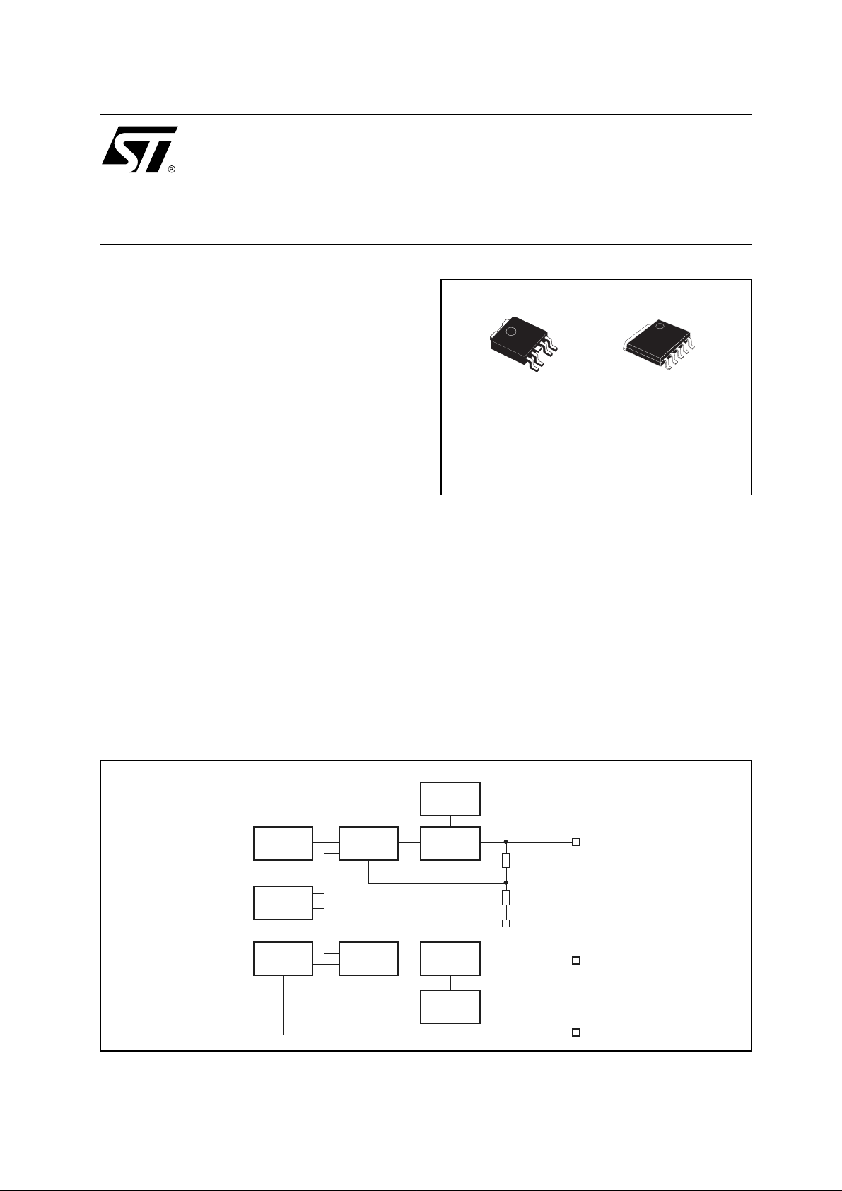
DESCRIPTION
Specifically designed for data storage
applications, this device integrates two voltage
regulators, each one able to supply 1A. It is
assembled in PPAK and in a new surface
mounting pa ckage named SPAK ( PowerFle x) at
5 pins. The first regulator block supply 3.3V to
power the Read Channel and Memory Chips
requiring this voltage. The second one is an
Adjustable output voltage from 1.25V to 3.0V that
PPAK
SPAK-5L
(PowerFlex
)
could power several kind of different
micro-controllers.
Both outputs are current limited and
overtemperature protected.
The very good thermal performances of the
package SPAK with only 2°C/W of Thermal
Resistance Junction to Case is important to
underline.
SCHEMATIC DIAGRAM
Thermal
Thermal
Protection
Protection
Err-Amp
Err-Amp
Err-Amp Power OutputVREF2
Err-Amp Power OutputVREF2
Over current
Over current
Protection
Protection
Power OutputVREF1
Power OutputVREF1
Over current
Over current
Protection
Protection
RA
RA
RB
RB
GND
GND
VOUT1
VOUT1
VOUT2
VOUT2
ADJ
ADJ
1/12March 2002
Page 2
ST2L01
ABSOLUTE MAXIMUM RATINGS
Symbol Parameter Value Unit
V
V
ESD
T
T
GENERAL OPERATING CONDITION
Symbol Parameter Value Unit
V
∆V
THERMAL DATA
Symbol Parameter SPAK-5L PPAK Unit
R
thj-case
Input Voltage
IN
ESD Tolerance (Human Body Model)
Storage Temperature Range
stg
Operating Junction Temperature Range
J
Input Voltage
IN
Input Voltage Ripple
IN
t
Input Voltage Rise Time (10% to 90%)
r
t
Input Voltage Fall Time (90% to 10%)
f
Thermal Resistance Junction-case
10 V
4KV
-55 to +125 °C
0 to +125 °C
4.75 to 5.25 V
±0.15 V
≥ 1 µs
≥ 1 µs
2 8 °C/W
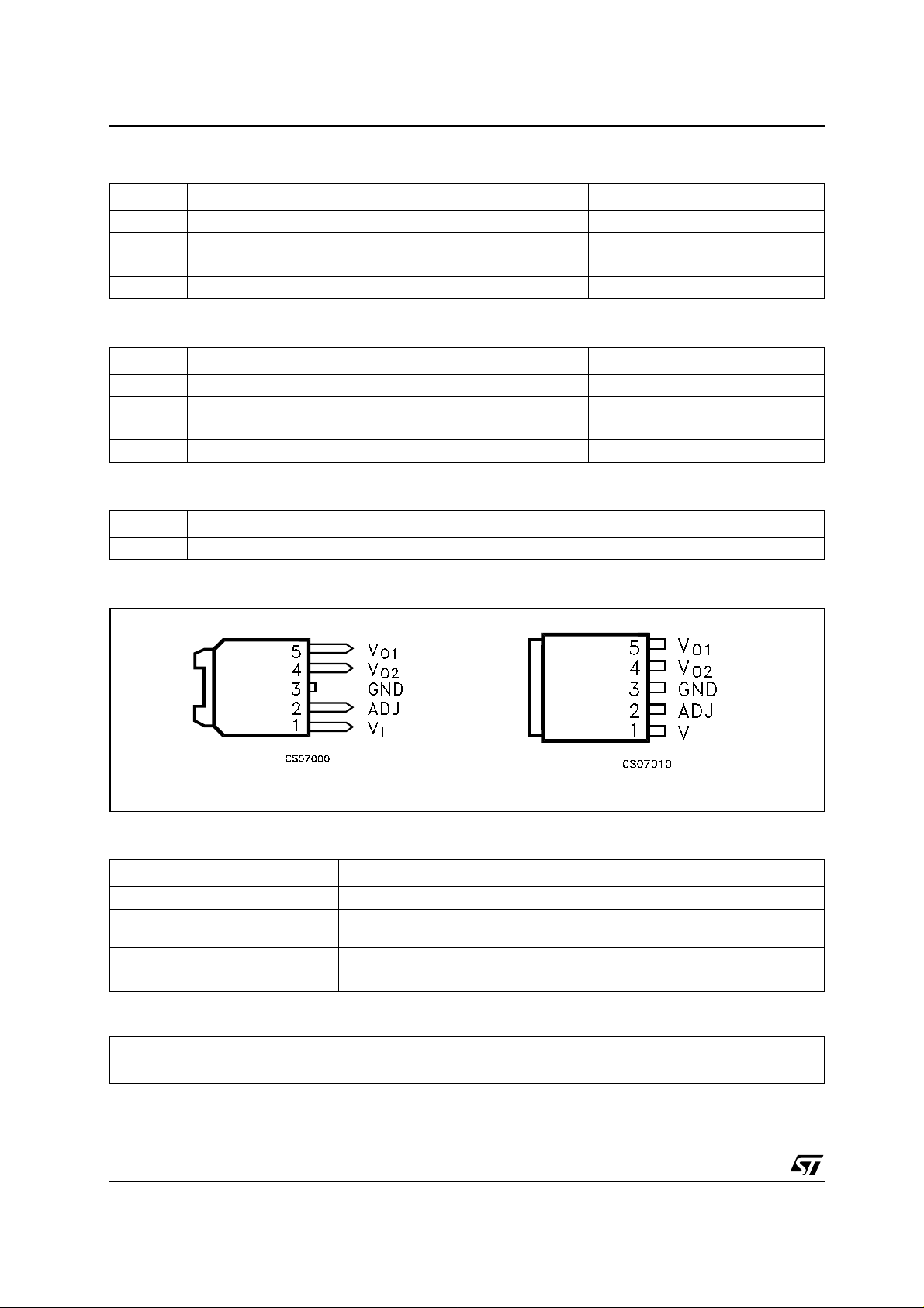
CONNECTION DIAGRAM (top view)
PPAK SPAK-5L
PIN DESCRIPTION
Pin N° Symbol Name and Function
1V
I
Input pin: bypass with a 1µF capacitor to GND
2 ADJ ADJ pin: resistor divider connection
3 GND Ground pin
4V
5V
O2
O1
Output Pin: adjustable output voltage; bypass with a 1µF capacitor to GND
Output Pin: fixed (3.3V) output voltage; bypass with a 1µF capacitor to GND
ORDERING INFORMATION
TYPE SPAK (Power Flex) 5 leads (*) PPAK (*)
ST2L01 ST2L01K5 ST2L01PT
(*) Avai l abl e in Tape & Re el wi th the suffix "R"
2/12
Page 3

ST2L01
TYPICAL APPLICATION CIRCUIT
R
VO = V
REF
Note:
C
value could be lowered down to 470n F Ceramic Capacitor (X7R);
O1
C
, CO1 and CO2 capacitors must be located not more than 0.5" from the outputs pins of t he device.
I
For mor e details about Capacitors read the "Application Hint s"
ELECTRICAL CHARACTERISTICS OF OUTPUT 1 (VI=5V, IO1=10mA Tj = 0 to 125°C unless otherwise
specified. Typical values are referred at T
Symbol Parameter Test Conditions Min. Typ. Max. Unit
I
Input Current IO1 = IO2 =0 Tj = 0 to 125°C 15 28 mA
I
V
Output Voltage 1 Tj = 25°C 3.23 3.3 3.37 V
O1
I
O1
T
∆V
∆V
SVR1 Supply Voltage Rejection V
∆V
∆V
Note 1: Low duty cycle p ul se testing wi t h Kelvin connections are required in order to maintain accurate data
Note 2: Dropout Voltage is defined as the minimum differential voltage between V
when the output voltage drops 1% below its nominal value.
Note 3: Transient response is defined with a step change in load from 10mA to 500mA as the time from the load step until the output voltage
reaches it’s minimum value.
Note 4: Min i m um lo ad current is defined as the minimum current requi red at the output in ord er for the output voltage to maintain regulation.
Note 5: Guaranteed by design, not tested in production.
Line Regulation 1 VI = 4.75 to 5.25V 0.1 6 mV
O1
Load Regulation 1 IO = 0.01 to 1A (Note 1) 3 12 mV
OUT1
V
Dropout Voltage 1 IO = 1A Tj = 0 to 125°C
D1
(Note 2)
t
Transient Response IO = 10 to 500mA t
TR
(Note 3, 5)
Current Limit 1 RL = 0 Tj = 0 to 125°C 1 A
I
SC1
I
Minimum Load Current 1 Tj = 0 to 125°C (Note 4) 0 mA
O1
I
O1
T
(Note 5)
Thermal Regulation I
O
eN1 Output Noise B= 10Hz to 10KHz (Note 5) 40 µVrms
Temperature Stability Tj = 0 to 125°C (Note 5) 0.5 %V
O1
Long Term Stability Tj = 125°C, 1000Hrs (Note 5) 0.3 %V
O1
= 25°C, CI = 1µF (Tantalum), CO1 = CO1 =1µF (X7R)
j
= 5mA to 1A VI = 4.75 to 5.25V
= 0 to 125°C
j
3.2 3.3 3.4
1.1 1.3 V
= t
= 1µs
fall
f
= 100Hz 60 68 dB
I
f
= 1KHz 60 70
I
f
= 10KHz 50 65
I
f
= 100KHz 30 38
I
= 30ms (Note 5) 0.1 %/W
and VO requir ed to m anta in re gulat ion at VO. It is measured
I
= 5 ±0.25V
I
= 100 mA
= 0 to 125°C
j
= 1A, t
rise
PULSE
<1 µs
1
(1 + )+I
R
2
ADJR1
O
O
3/12
Page 4

ST2L01
ELECTRICAL CHARACTERISTICS OF OUTPUT 2 (VI=5V, IO2=10mA Tj = 0 to 125°C unless otherwise
specified. Typical values are referred at T
"Typical Application Circuit "figure with R
Symbol Parameter Test Conditions Min. Typ. Max. Unit
V
Operating Input Voltage IO2 =5mA to 1A Tj = 0 to 125°C 4.5 V
I
V
Output Voltage 2 Tj = 25°C 2.45 2.5 2.55 V
O2
V
∆V
∆V
∆I
SVR2 Supply Voltage Rejection V
∆V
∆V
Note 1: Low duty cycle p ul se testing wi t h Kelvin connections are required in order to maintain accurate data
Note 2: Dropout Voltage is defined as the minimum differential voltage between V
when the output voltage drops 1% below its nominal value.
Note 3: Transient response is defined with a step change in load from 10mA to 500mA as the time from the load step until the output voltage
reaches it’s minimum value.
Note 4: Min i m um lo ad current is defined as the minimum current requi red at the output in ord er for the output voltage to maintain regulation.
Note 5: Guaranteed by design, not tested in production.
Reference Voltage
REF
(measured between pins 4
and 2)
Line Regulation 2 VI = 4.75 to 5.25V 0.004 0.2 %
O2
Load Regulation 2 IO = 0.01 to 1A (Note 1) 0.08 0.4 %
O2
V
Dropout Voltage 2 IO = 1A Tj = 0 to 125°C
D2
Tj = 25°C 1.225 1.25 1.275 V
I
T
(Note 2)
Transient Response IO = 10 to 500mA t
t
TR
(Note 3, 5)
I
Current Limit 2 RL = 0 Tj = 0 to 125°C 1 A
SC2
I
Minimum Load Current 2 Tj = 0 to 125°C (Note 4) 1 mA
O2
I
Adjust Pin Current Tj = 0 to 125°C 35 120 µA
ADJ
Adjust Pin Current IO1 = 5mA to 1A VI = 4.75 to 5.25V
ADJ
T
I
T
(Note 5)
Thermal Regulation 2 I
eN2 Output Noise 1 B= 10Hz to 10KHz (Note 5) 30 µVrms
Temperature Stability Tj = 0 to 125°C (Note 5) 0.5 %V
REF
Long Term Stability Tj = 125°C, 1000Hrs (Note 5) 0.3 %V
REF
= 25°C, CI = 1µF (Tantalum), CO1 = CO1 =1µF (X7R). Refer to
j
=120Ω".
1=R2
= 5mA to 1A VI = 4.75 to 5.25V
O1
= 0 to 125°C
j
1.2125 1.25 1.2875
1.1 1.3 V
= t
rise
fall
= 1µs
<1 µs
05µA
= 0 to 125°C
j
= 5 ±0.25V
I
= 100 mA
O1
= 0 to 125°C
j
= 1A, t
O
PULSE
f
= 100Hz 70 77 dB
I
f
= 1KHz 70 80
I
f
= 10KHz 50 65
I
f
= 100KHz 30 43
I
= 30ms (Note 5) 0.1 %/W
and VO requir ed to m anta in re gulat ion at VO. It is measured
I
O
O
4/12
Page 5

APPLICATION HINTS
ST2L01
EXTERNAL CAPACITORS
Like any low-dropout regulator, the ST2L01
requires external capacitors for stability. We
suggest to solder both capacitors as close as
possible to the relative pins (1, 2 and 5).
INPUT CAPACITORS
An input capacitor, whose value is at least 1µF, is
required; the amount of the input capacitance c an
be increased without limit if a good quality
tantalum or aluminum capacitor is used.
SMS X7R or Y5V ceramic multilayer capacitors
could not ensure stability in any condition because
of their variable characteristics with Frequency
and Temperature; the use of this capacitor is
strictly related to t he us e of the output c ap ac itors.
For more details read the "OUTPUT CAPACITOR
SECTION".
The input capacitor must be located at a distance
of not more than 0.5" from the input pin of the
device and returened to a clean analog ground.
OUTPUT CAPACITOR
The ST2L01 is designed specifically to work with
Ceramic and Tantalum capacitros.
Special care must be taken when a Ceramic
multilayer capacitor is used.
Special care must be taken when a Ceramic
multilayer capacitor is used.
Due to their characteristics they can sometimes
have an ESR value lower than the minimum
required by the ST2 L01 and their relatively large
capacitance can change a lot with the ambient
temperature.
The test results of the ST2L01 stability using
multilayer ceramic capacitors show that a
minimum value of 1µF is needed for the adjustable
regulator (set to 2.5V). This value can be
increased up t o 10µF wh en a tantalum capacitor
is used on the inp ut. A higher v alue C
can have
O
an ESR lower than the accepted minimum.
When a ceramic capacitor is used on the input the
output capacitance must be in the range from 1µF
to 2.2µF if C
C
=2.2µF.
I
=1µF, and from 1µF to 4.7µF if
I
The 3.3V regulator stable with a 470nF capacitor.
This value can be increased up to 10µF if a
tantalum capacitor is used on the input. A higher
value C
can have an ESR lower than the
O
accepted minimum.
When a ceramic capac itor is used in the input the
output capacitance must be in the range from 1µF
to 2.2µF if C
C
=2.2µF.
I
=1µF, and from 1µF to 4.7µF if
I
Surface-mountable solid tantalum capacitors offer
a good combination of small physical size for the
capacitance value and ESR in the range needed
by the ST2L01. The test results show good
stability for both outputs with values of at least
1µF. The value can be increased without limit for
even better performance such a transient
response and noise.
IMPORTANT; The output capacitor must maintain
its ESR in the stable region over the full operating
temperature to assure stability. Also , capacitor
tolerance and variation with temperature must be
considered to assure that the minimum amount of
capacitance is provided at all times. For this
reason, when a ceramic multilayer capacitor is
used, the better choise for temperatu re coefficent
is the X7R type, which holds the capacitance
within ±15% . The output capacitor should be
located not more than 0.5" from the ou tput pins of
the device and returned to a clean analog ground.
ADJUSTABLE REGULATOR
The ST2L01 has a 1.25V reference voltage
between the output and the adjustable pins
(respectevely pin 4 and 2). When a resistor R2 is
placed between these two t herminals a constant
current flows through R2 and down to R1 to set
the overall (V
to GND) output voltage.
O2
Minimum load current is 1mA.
I
is very small (typically 35µA) and constant; in
ADJ
the V
calculation it can be ignored.
O
5/12
Page 6

ST2L01
TYPICAL CHARACTERISTICS (CI=1µF, CO=1µF (X7R))
Figure 1 : Input Current vs Temperature
Figure 2 : Input Current vs Input Voltage
Figure 4 : Load Regulation vs Temperature
Figure 5 : Output Voltage vs Input Voltage
Figure 3 : Output Voltage vs Temperature
6/12
Figure 6 : Dropout Voltage vs Temperature
Page 7

ST2L01
Figure 7 : Line Regulation vs Temperature
Figure 8 : Supply Voltage Rejection vs
Frequency
Figure 10 : Dropout Voltage vs Output Current
Figure 11 : Reference Voltage vs Temperature
Figure 9 : Supply Voltage Rejection vs
Temperature
Figure 12 : Output Voltage vs Input Voltage
7/12
Page 8

ST2L01
Figure 13 : Line Regulation vs Temperature
Figure 14 : Load Regulation vs Temperature
Figure 16 : Dropout Voltage vs Temperature
Figure 17 : Dropout Voltage vs Output Current
Figure 15 : Supply Voltage Rejection vs
Temperature
8/12
Figure 18 : Supply Voltage Rejection vs
Frequency
Page 9

ST2L01
V
I
C
F(X7R), T
°C
V
V
I
C
F(X7R)
V
V
I
500mA, C
F(X7R)
V
I
C
F(X7R)
Figure 19 : Adjustable pin vs Temperature
Figure 20 : Minimum Load Current vs
Temperature
Figure 22 : Load Transient
=5V,
I
T
J
=adjusted to 2.5V,
O
=25°C
=500 to 10mA,
O
Figure 23 : Load Transient
O
=1µ
Figure 21 : Load Transient
=5V,
I
=500 to 10mA,
O1
O
=1µ
J
=25
=5V,
I
O
=adjusted to 2.5V,
=10 to
O2
Figure 24 : Load Transient
=5V,
I
=10 to 500mA,
O1
=1µ
O
=1µ
O
9/12
Page 10

ST2L01
SPAK-5L MECHANICAL DATA
DIM.
A 1.78 2.03 0.070 0.080
A2 0.03 0.13 0.001 0.005
C 0.25 0.010
C1 0.25 0.010
D 1.02 1.27 0.040 0.050
D1 7.87 8.13 0.310 0.320
F 0.63 0.79 0.025 0.031
G 1.69 0.067
G1 6.8 0.268
H1 5.59 0.220
H2 9.27 9.52 0.365 0.375
H3 8.89 9.14 0.350 0.360
L 10.41 10.67 0.410 0.420
L1 7.49 0.295
L2 8.89 9.14 0.350 0.360
M 0.79 1.04 0.031 0.041
N 0.25 0.010
V3˚ 6˚3˚ 6˚
MIN. TYP MAX. MIN. TYP. MAX.
mm. inch
10/12
PO13F1/B
Page 11

PPAK MECHANICAL DATA
ST2L01
DIM.
MIN. TYP MAX. MIN. TYP. MAX.
A 2.2 2.4 0.086 0.094
A1 0.9 1.1 0.035 0.043
A2 0.03 0.23 0.001 0.009
B 0.4 0.6 0.015 0.023
B2 5.2 5.4 0.204 0.212
C 0.45 0.6 0.017 0.023
C2 0.48 0.6 0.019 0.023
D 6 6.2 0.236 0.244
E 6.4 6.6 0.252 0.260
G 4.9 5.25 0.193 0.206
G1 2.38 2.7 0.093 0.106
H 9.35 10.1 0.368 0.397
L2 0.8 0.031
L4 0.6 1 0.023 0.039
mm. inch
0078180-B
11/12
Page 12

ST2L01
Information furnished is believed to be accurate and reliable. However, STMicroelectronics assumes no responsibility f or the
consequences of use of such informatio n nor for any infringement of paten ts or o ther rig hts of t hird part ies which ma y result from
its use. No license is granted by implication or otherwise under any patent or patent rights of STMicroelectronics. Specifications
mentioned in this publication are subject to change without notice. This publication supersedes and replaces all information
previousl y suppl ied. STM icroel ectronics produc ts are not auth orized for use as c ritica l compone nts in l ife s upport dev ices or
systems without express written approval of STMicroelectronics.
Australia - Brazil - Canada - China - Finland - France - Germany - Hong Kong - India - Israel - Italy - Japan - Malaysia - Malta - Morocco
© The ST logo is a registered trademark of STMicroelectronics
© 2002 STMicroelectronics - Printed in Italy - All Rights Reserved
STMicroelectronics GROUP OF COMPANIES
Singapore - Spain - Sweden - Switzerland - United Kingdom - United States.
© http://www.st.com
12/12
 Loading...