

Page 1
ST24LC21B, ST24LW21
ST24FC21, ST24FC21B, ST24F W21
1 Kbit (x8) Dual Mode Serial EEPROM
for VESA PLUG & P LAY
June 2002 1/22
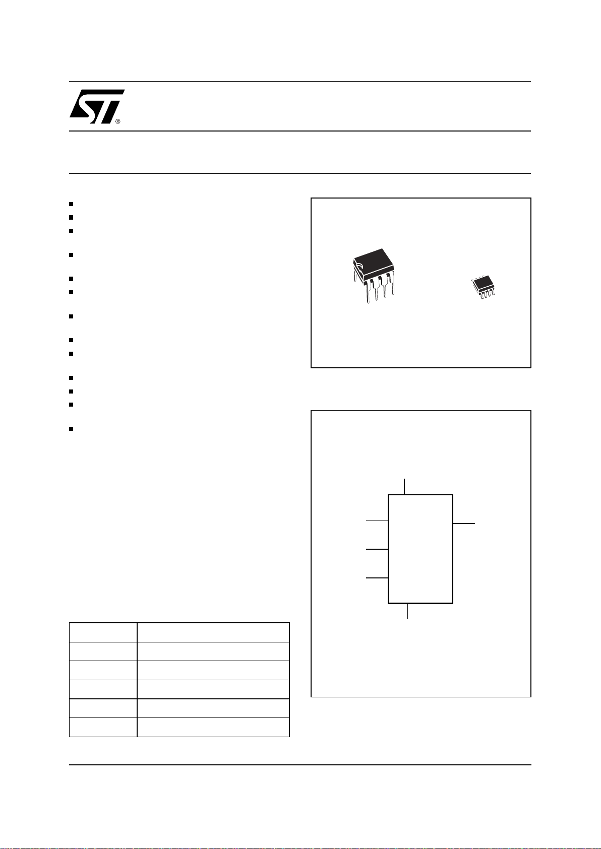
AI01741
SDA
V
CC
ST24xy21VCLK
SCL
V
SS
WC
Figure 1. Logic Diagram
1 MILLION ERASE/WRITE CYCLES
40 YEARS DATA RETENTION
3.6V to 5.5V or 2.5V to 5.5V SINGLE SUPPLY
VOLT AGE
HARDWARE WRITE CONTROL (ST24LW21
and ST24FW21)
TTL SCHMITT-TRIGGER on VCLK INPUT
100k / 400k Hz COMPATIBILITY with the I2C
BUS BIT TRANSFER RANGE
TWO WIRE SERIAL INTERFACE I2C BUS
COMPATIBLE
I2C PAGE WRITE (up to 8 Bytes)
I2C BYTE, RANDOM and SEQUENTIAL READ
MODES
SELF TIMED PROGRAMMING CYCLE
AUTOMATIC ADDRESS INCREMENTING
ENHANCED ESD/LATCH UP
PERFORMANCES
ERROR RECOVERY MECHANISM
(ST24FC21 and ST24FW21) VESA 2
COMPATIBLE
DESCRIPTION
The ST24LC21B, ST24LW21, ST24FC21,
ST24FC21B and ST24FW21 are 1K bit electrically
erasable programmable memory (EEPROM), organized in 128x8 bits. In the text, products are
referred as ST24xy21, where "x" is either "L" for
VESA 1 or "F" for VESA 2 compatible memories
and where "y" indicates the Write Control pin connection: "C" means WC on pin 7 and "W" means
WC on pin 3.
SDA Serial Data Address Input/Output
SCL Serial Clock (I
2
C mode)
V
CC
Supply Voltage
V
SS
Ground
VCLK Clock Transmit only mode
WC Write Control
Table 1. Signal Names
8
1
SO8 (M)
150mil Width
8
1
PSDIP8 (B)
0.25mm Frame
Note: WC signal is on ly a v a ila b le f o r ST24LW21 and ST24FW21
products.
Page 2
SDAV
SS
SCL
VCLKNC
NC V
CC
NC
AI01742
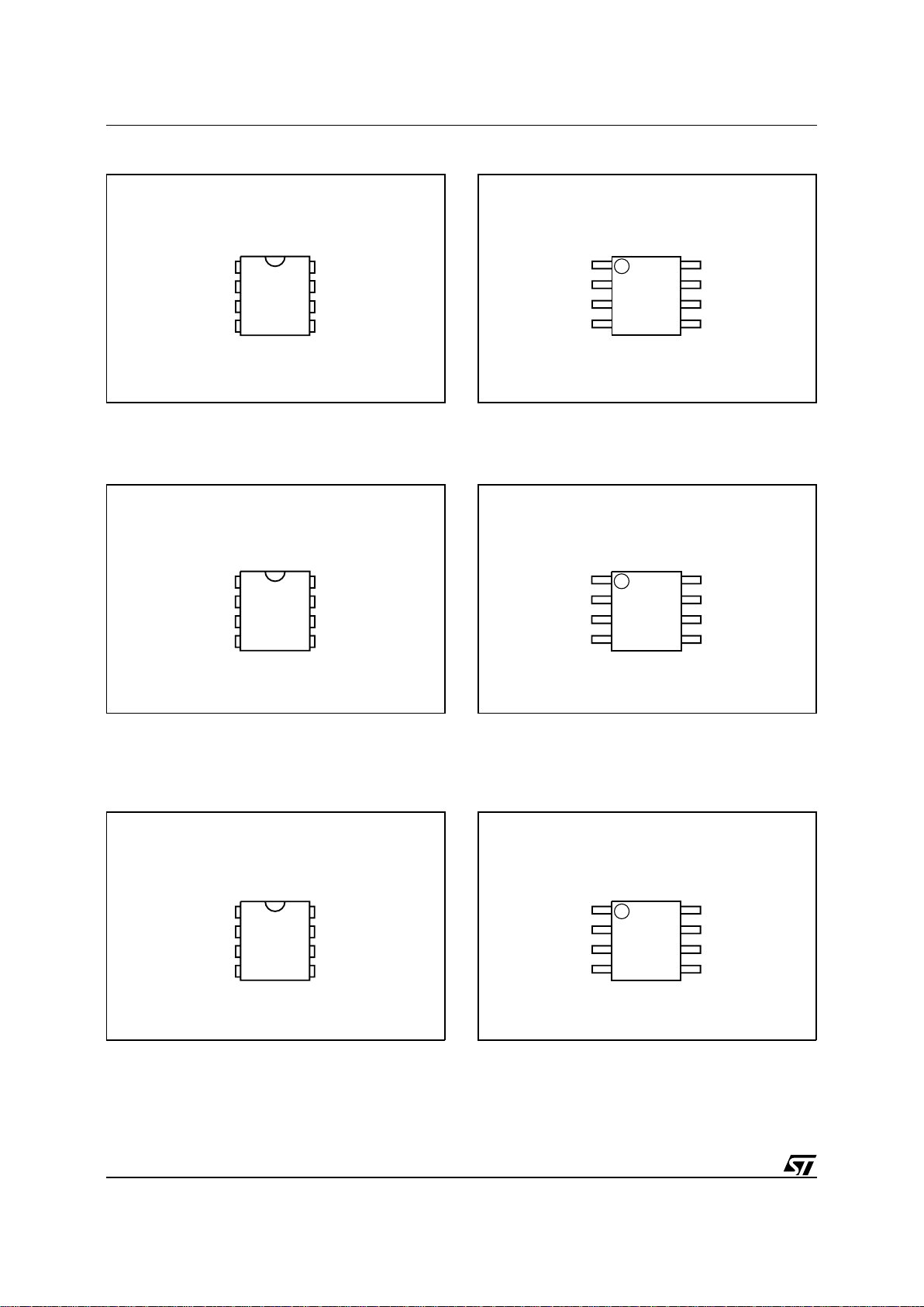
ST24LC21B
1
2
3
4
8
7
6
5
Figure 2A. DIP Pin Connections
1
AI01743
2
3
4
8
7
6
5
SDAV
SS
SCL
VCLKNC
NC V
CC
NC
ST24LC21B
Figure 2B. SO Pin Connections
Warning: NC = Not Connected. Warning: NC = Not Connected.
SDAV
SS
SCL
VCLKNC
NC V
CC
DU
AI01744
ST24FC21
ST24FC21B
1
2
3
4
8
7
6
5
Figure 2C. DIP Pin Connections
1
AI01745
2
3
4
8
7
6
5
SDAV
SS
SCL
VCLKNC
NC V
CC
DU
ST24FC21
ST24FC21B
Figure 2D. SO Pin Connections
Warning: NC = Not Connected. DU = Don’t Use, must
be left open or connected to V
CC
or VSS.
SDAV
SS
SCL
VCLKNC
NC V
CC
WC
AI01746
ST24FW21
ST24LW21
1
2
3
4
8
7
6
5
Figure 2E. DIP Pin Connections
1
AI01747
2
3
4
8
7
6
5
SDAV
SS
SCL
VCLKNC
NC V
CC
WC
ST24FW21
ST24LW21
Figure 2F. SO Pin Connections
Warning: NC = Not Connected. Warning: NC = Not Connected.
Warning: NC = Not Connected. DU = Don’t Use, must
be left open or connected to V
CC
or VSS.
2/22
ST24LC21B, ST24LW21, ST24FC21, ST24FC21B, ST24FW21
Page 3
Symbol Parameter Value Unit
T
A
Ambient Operating Temperature –40 to 85 °C
T
STG
Storage Temperature –65 to 150 °C
T
LEAD
Lead Temperature, Soldering (SO8 package)
(PSDIP8 package)
40 sec
10 sec
215
260
°C
V
IO
Input or Output Voltages –0.3 to 6.5 V
V
CC
Supply Voltage –0.3 to 6.5 V
V
ESD
Electrostatic Discharge Voltage (Human Body model)
(2)
4000 V
Electrostatic Discharge Voltage (Machine model)
(3)
500 V
Notes: 1. Except for the rating "Operating Temperature Range", stresses above those listed in the Table "Absolute Maximum Ratings"
may ca use permanent damage to the device. These are stress ratings only and operation of the device at these or any other
conditions above those indicated in the Operating sections of this specification is not implied. Exposure to Absolute Maximum
Rating conditions for extended periods may affect device reliability. Refer also to the STMicroelectronics SURE Program and other
relevant quality docum ent s.
2. MIL-STD-883C, 3015.7 (100pF , 1500 Ω).
3. EIAJ IC-121 (Condition C) (200pF, 0 Ω).
Table 2. Absolute Maximum Ratings
(1)
Device Code Chip Enable RW
Bit b7 b6 b5 b4 b3 b2 b1 b0
Device Select 1 0 1 0 X X X R
W
Note: The MSB b7 is sent first.
X = 0 or 1.
Table 3A. Device Select Code (ST24LC21B, ST24LW21, ST24FC21 and ST24FW21)
The ST24xy21 can operate in two modes: Transmit-Only mode and I
2
C bidirectional mode. When
powered, the device is in Transmit-Only mode with
EEPROM data clocked out from the rising edge of
the signal applied on VCLK.
The device will switch to the I
2
C bidirectional mode
upon the falling edge of the signal applied on SCL
pin. When in I
2
C mode, the ST24LC21B (or the
ST24LW21) cannot switch back to the Transmit
Only mode (except when the power supply is removed). For the ST24FC21, ST24FC21B (or the
ST24FW21), after the falling edge of SCL, the
memory enter in a transition state which allowed to
switch back to the Transmit-Only mode if no valid
I
2
C activity is observed. Both Plastic Dual-in -Line
and Plastic Small Outline packages are available.
Transmit Only Mode
After a Power-up, the ST24xy21 is in the Tra nsmit
Only mode. A proper initialization sequence (see
Figure 3) must supply nine clock pulses on the
VCLK pin (in order to internally synchronize the
device). During this initialization sequence, the
SDA pin is in high im pedance. On the rising edge
of the tenth pulse applied on VCLK pin, the device
will output the first bit of byte located at address 00h
(most significant bit first).
DESCRIPTION (cont’d)
Device Code Chip Enable RW
Bit b7 b6 b5 b4 b3 b2 b1 b0
Device Select 1 010000R
W
Note: The MSB b7 is sent first.
X = 0 or 1.
Table 3B. Device Select Code (ST24FC21B)
3/22
ST24LC21B, ST24LW21, ST24FC21, ST24F C21B, ST24FW21
Page 4
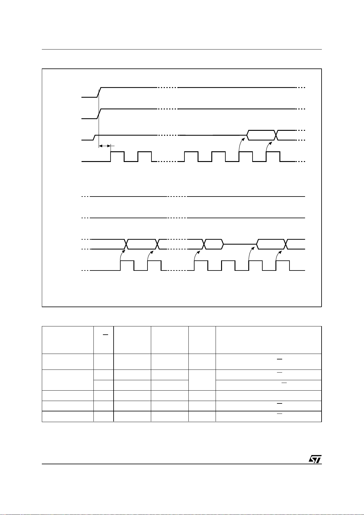
AI01501
Bit 7
V
CC
tVPU
SCL
SDA
VCLK
Bit 6
Bit 7
V
CC
SCL
SDA
VCLK
Bit 6
Bit 6 Bit 4 Bit 0
12 891011
12 13 17 18 19 20
Bit 5
Figure 3. Transmit Only Mode Waveforms
Mode
R
W
bit
ST24LC21B
ST24FC21
ST24FC21B
VCLK
ST24LW21
ST24FW21WCBytes Initial Sequence
Current Address
Read
’1’ X X 1 START, Device Select, R
W = ’1’
Random Address
Read
’0’ X X
1
START, Device Select, RW = ’0’, Address,
’1’ X X reSTART, Device Select, R
W = ’1’
Sequential Read ’1’ X X 1 to 128 Similar to Current or Random Mode
Byte Write ’0’ V
IH
V
IH
1 START, Device Select, RW = ’0’
Page Write ’0’ V
IH
V
IH
8 START, Device Select, RW = ’0’
Note: X = VIH or V
IL
T able 4. I2C Operating Modes
4/22
ST24LC21B, ST24LW21, ST24FC21, ST24FC21B, ST24FW21
Page 5
A byte is clocked out (on SDA pin) with nine clock
pulses on VCLK: 8 clock pulses for the data byte
and one extra clock pulse for a Don’t Care bit.
As long as the SCL pin is held high, each byte of
the memory array is transmitted serially on the SDA
pin with an automatic address increment.
When the last byte is transmitted, the address
counter will roll-over to location 00h.
I
2
C Bidirectional Mode
The ST24xy21 can be switched from T ransmit Only
mode to I
2
C Bidirectional mode by applying a valid
high to low transition on the SCL pin (see Figure 4).
– When the ST24LC21B (or the ST24FC21 or
the ST24FC21B) is in the I
2
C Bidirectional
mode, the VCLK input (pin 7) enables (or inhibits) the execution of any write instruction: if
VCLK = 1, write instructions are executed; if
VCLK = 0, write instructions are not executed.
– When the ST24LW 21 (or the ST24FW21) is in
the I
2
C Bidirectional mode, the Write Control
(WC on pin 3) input enables (or inhibits) the
execution of any write instruction: if WC = 1,
write instructions are executed;if WC = 0,
write instructions are not executed.
The ST24xy21 is compatible with the I
2
C standard,
two wire serial interface which uses a bidirectional
data bus and serial clock. The ST24xy21 carries a
built-in 4 bit, unique device identification code
(1010) named Dev ice Select code corresponding
to the I
2
C bus definition. The ST24LC21B carries a
unique device identification code (1010.0000 R
W)
named Device Select code corresponding to the
I
2
C bus definition.
The ST24xy21 behaves as a slave dev ice in the
I
2
C protocol with all memory operations synchronized by the serial clock SCL. Read and write
operations are initiated by a STAR T condition generated by the bus master. The START condition is
followed by a stream of 7 bits, plus one read/write
bit and terminated by an acknowledge bit.
When data is written into the memory, the
ST24xy21 responds to the 8 bits received by asserting an acknowledge bit during the 9th bit time.
When data is read by the bus master, it must
acknowledge the receipt of the data bytes in the
same way. Data transfers are terminated with a
STOP condition (see READ and WRITE desc riptions in the following pages).
Power On Reset: V
CC
lock out write protect
In order to prevent data corruption and inadvertent
write operations during power up, a Power On
Reset (POR) circuit is implement ed. Until the V
CC
voltage has reached the POR threshold value, the
internal reset is active, all operations are disabled
and the device will not respond to any c ommand.
In the same way, when V
CC
drops down from the
operating voltage to below the POR threshold
value, all operations are disabled and the dev ice
will not respond to any command. A stable V
CC
must be applied before applying any logic signal.
Error Recovery Modes available in the
ST24FC21, ST24FC21B and the ST24FW21
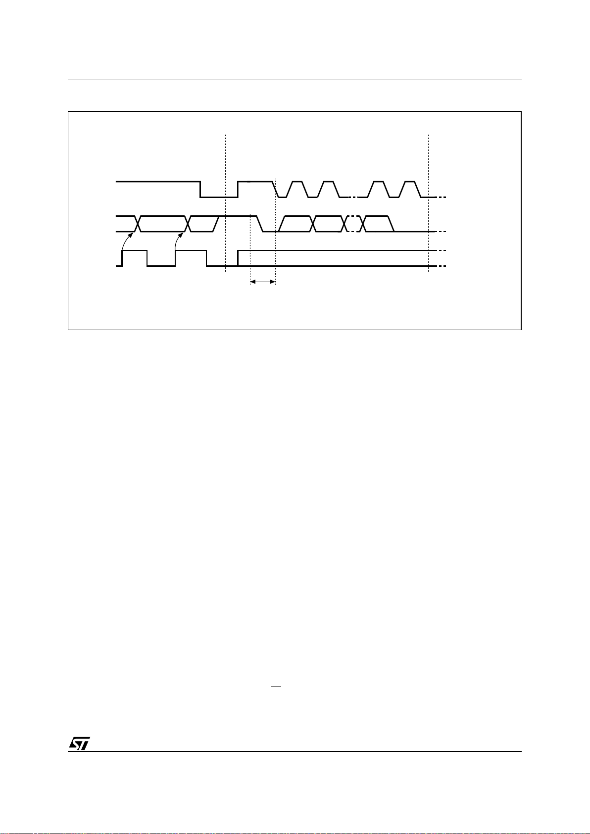
AI01892
SCL
SDA
VCLK
Transmit Only Mode
1
2 89
MSB
ACK
START
CONDITION
- Temporary Bi-Directional Mode
(ST24FC21 and ST24FW21)
- Locked Bi-Directional Mode
(ST24LC21B and ST24LW21)
- Locked Bi-Directional
Mode (ST24FC21
and ST24FW21)
Figure 4. Transition from Transmit Only (DDC1) to Bi-directional (DDC2B) Mode Waveforms
5/22
ST24LC21B, ST24LW21, ST24FC21, ST24F C21B, ST24FW21
Page 6
AI01748
Switch Back to
Transmit-Only Mode
Memory Power On
Internal Address Pointer = 0
VCLK
YES
NO
NO
Send Data bit (MSB first) pointed
by the Address Pointer and
auto-increment pointed bit/byte
SCL
YES
NO
SDA Hi-Z
VCLK Internal Counter = 0
Start Internal 2 sec Timer
SCL
YES
Reset VCLK Internal Counter
and Reset Internal Timer
Valid
I
2
C access
(START + Device Select)
?
YES
VCLK
YES
Increment VCLK Counter
Counter = 128
or Timer > 2 sec
YES
I2C communication idle
waiting for a Device Select byte
Reset Counter and Timer
Send Acknowledge
Respond to the Incoming
I
2
C Command
Transition
State
(VESA 2)
Transmit-Only Mode
(DDC1)
I2C Mode
(DDC2B)
NO
NO
Figure 5. Error Recovery Mechanism Flowchart for the ST24FC21, ST24FC21B and ST24FW21
products
6/22
ST24LC21B, ST24LW21, ST24FC21, ST24FC21B, ST24FW21
Page 7
AI01665
V
CC
C
BUS
SDA
R
L
MASTER
R
L
SCL
C
BUS
100
0
4
8
12
16
20
C
BUS
(pF)
Maximum RP value (kΩ)
10 1000
fc = 400kHz
fc = 100kHz
Figure 6. Maximum RL Value versus Bus Capacitance (C
BUS
) for an I2C Bus
When the ST24FC21 (or the ST24FC21B or t he
ST24FW21) first switches to the I
2
C mode (VESA
DDC2B mode), it enters a transition state which is
functionally identical to I
2
C operation. But, if the
ST24FC21 (or the ST 24FC21B or the ST24FW21)
does not receive a valid I
2
C sequence, that is a
ST AR T condition followed by a valid Device Select
code (1010XXX R
W for ST24FC21 and
ST24FW21; 1010000 R
W for ST24FC21B), within
either 128 VCLK periods or a period of time of
t
RECOVERY
(approximately 2 seconds), the
ST24FC21 (or the ST 24FC21B or the ST24FW21)
will revert to the Transmit-Only m ode (VESA DDC1
mode).
If the ST24FC21 (or the ST24FC21B or the
ST24FW21) decodes a valid I
2
C Device Select
code, it will lock into I
2
C mode. Under this condition,
signals applied on the VCLK input will not disturb
READ access from the ST24FC21 (or the
ST24FC21B or the ST24FW21). For WRITE access, refer to the Signal Description paragraph.
When in the transition state, the count of VCLK
pulses and the internal 2 seconds timer are reset
by any activity on the SCL line. This me ans that,
after each high to low transition on SCL, the memory will re-initialise its transition state and will switch
back to Transmit-Only mode only after 128 more
VCLK pulses or after a new t
RECOVERY
delay.
SIGNAL DESCRIPTIONS
I
2
C Serial Clock (SCL). The SCL input pin is used
to synchronize all data in and out of the memory. A
resistor can be connected from the SCL line to V
CC
to act as a pull up (see Figure 6).
Serial Data (SDA). The SDA pin is bi-directional
and is used to transfer data in or out of the memory.
It is an open drain output that may be wire-OR’ed
with other open drain or open collector signals on
the bus. A resistor must be connected from the SDA
bus line to V
CC
to act as pull up (see Figure 6).
Tr ansmit Only Clock (VCLK). The VCLK input pin
is used to synchronize data out when the ST24xy21
is in Transmit Only mode.
For the ST24LC21B and the ST24FC21 or
ST24FC21B Only, the VCLK offers also a Write
Enable (active high) function when the ST24LC21B
and the ST24FC21 or ST24FC21B are in I
2
C bidi-
rectional mode.
Write Control (WC). An hardware Wri te Control
feature (WC) is offered only on ST24LW21 and
ST24FW21 on pin 3. This feature is usefull to
protect the contents of the memory from any erroneous erase/write cycle. The Write Control signal
is used to enable (WC = V
IL
) or disable (WC = VIH)
the internal write protection. When unconnected,
the WC input is internally tied to V
SS
by a 100k ohm
pull-down resistor and the memory is write protected.
DEVICE OPERATION
7/22
ST24LC21B, ST24LW21, ST24FC21, ST24F C21B, ST24FW21
Page 8

Symbol Parameter Test Condition Min Max Unit
C
IN
Input Capacitance (SDA) 8 pF
C
IN
Input Capacitance (other pins) 6 pF
t
LP
Low-pass filter input time constant
(SDA and SCL)
200 500 ns
Note: 1. Sampled only, not 100% tested.
Table 5. Input Parameters
(1)
(TA = 25 °C, f = 100 kHz )
Symbol Parameter Test Condition Min Max Unit
I
LI
Input Leakage Current 0V ≤ VIN≤ V
CC
±2 µA
I
LO
Output Leakage Current
0V ≤ V
OUT
≤ V
CC
SDA in Hi-Z
±2 µA
I
CC
Supply Current
V
CC
= 5V, fC = 400kHz
(Rise/Fall time < 10ns)
2mA
Supply Current V
CC
= 3.6V, fC = 400kHz 1 mA
I
CC1
Supply Current (Standby)
V
IN
= VSS or VCC,
V
CC
= 5V, fC = 0
100 µA
V
IN
= VSS or VCC,
V
CC
= 5V, fC = 400kHz
300 µA
I
CC2
Supply Current (Standby)
V
IN
= VSS or VCC,
V
CC
= 3.6V, fC = 0
30 µA
V
IN
= VSS or VCC,
V
CC
= 3.6V, fC = 400kHz
100 µA
V
IL
Input Low Voltage
(SCL, SDA, WC)
–0.3 0.3 V
CC
V
V
IH
Input High Voltage
(SCL, SDA, WC)
0.7 V
CC
VCC + 1 V
V
P
High Level Threshold Voltage
(Schmitt Trigger on VLCK)
V
CC
= 5.5V 1.4 2.1 V
V
CC
= 4.5V 1.2 1.9 V
V
CC
= 3.6V 1 1.7 V
V
N
Low Level Threshold Voltage
(Schmitt Trigger on VLCK)
V
CC
= 5.5V 0.6 1.4 V
V
CC
= 4.5V 0.5 1.2 V
V
CC
= 3.6V 0.4 1 V
V
H
Hysteresis Voltage
(Schmitt Trigger on VLCK)
V
CC
= 5.5V 0.4 1.5 V
V
CC
= 4.5V 0.4 1.4 V
V
CC
= 3.6V 0.35 1.3 V
V
OL
Output Low Voltage
I
OL
= 3mA, VCC = 3.6V 0.4 V
I
OL
= 6mA, VCC = 5V 0.6 V
Table 6A. DC Characteristics (ST24LC21B, ST24LW21, ST24FC21 and ST24FW21)
(T
A
= –40 to 85 °C; VCC = 3.6V to 5.5V)
8/22
ST24LC21B, ST24LW21, ST24FC21, ST24FC21B, ST24FW21
Page 9

Symbol Parameter Test Condition Min
(1)
Max
(1)
Unit
I
LI
Input Leakage Current 0V ≤ VIN≤ V
CC
±2 µA
I
LO
Output Leakage Current
0V ≤ V
OUT
≤ V
CC
SDA in Hi-Z
±2 µA
I
CC
Supply Current
V
CC
= 5V, fC = 400kHz
(Rise/Fall time < 10ns)
2mA
Supply Current V
CC
= 2.5V, fC = 400kHz 1 mA
I
CC1
Supply Current (Standby)
V
IN
= VSS or VCC,
V
CC
= 5V, fC = 0
100 µA
V
IN
= VSS or VCC,
V
CC
= 5V, fC = 400kHz
300 µA
I
CC2
Supply Current (Standby)
V
IN
= VSS or VCC,
V
CC
= 2.5V, fC = 0
30 µA
V
IN
= VSS or VCC,
V
CC
= 2.5V, fC = 400kHz
100 µA
V
IL
Input Low Voltage
(SCL, SDA, WC)
–0.3 0.3 V
CC
V
V
IH
Input High Voltage
(SCL, SDA, WC)
0.7 V
CC
VCC + 1 V
V
P
High Level Threshold Voltage
(Schmitt Trigger on VLCK)
V
CC
= 5.0V 1.2 1.9 V
V
CC
= 2.5V 0.8 1.4 V
V
N
Low Level Threshold Voltage
(Schmitt Trigger on VLCK)
V
CC
= 5.0V 0.6 1.7 V
V
CC
= 2.5V 0.5 1.1 V
V
OL
Output Low Voltage
I
OL
= 2.1mA, VCC = 2.5V 0.4 V
I
OL
= 6mA, VCC = 5V 0.6 V
Note 1: Preliminary results.
Table 6B. DC Characteristics (ST24FC21B)
(T
A
= –40 to 85 °C; VCC = 2.5 to 5.5V)
9/22
ST24LC21B, ST24LW21, ST24FC21, ST24F C21B, ST24FW21
Page 10

Symbol Alt Parameter Min Max Unit
t
CH1CH2
(1)
t
R
Clock Rise Time 300 ns
t
CL1CL2
(1)
t
F
Clock Fall Time 300 ns
t
DH1DH2
(1)
t
R
SDA Rise Time 20 300 ns
t
DL1DL2
(1)
t
F
SDA Fall Time 20 300 ns
t
CHDX
(2)
t
SU:STA
Clock High to Input Transition 600 ns
t
CHCL
t
HIGH
Clock Pulse Width High 600 ns
t
DLCL
t
HD:STA
Input Low to Clock Low (START) 600 ns
t
CLDX
t
HD:DAT
Clock Low to Input Transition 0 µs
t
CLCH
t
LOW
Clock Pulse Width Low 1.3 µs
t
DXCX
t
SU:DAT
Input Transition to Clock Transition 100 ns
t
CHDH
t
SU:STO
Clock High to Input High (STOP) 600 ns
t
DHDL
t
BUF
Input High to Input Low (Bus Free) 1.3 µs
t
CLQV
t
AA
Clock Low to Data Out Valid 200 900 ns
t
CLQX
t
DH
Clock Low to Data Out Transition 200 ns
f
C
f
SCL
Clock Frequency 400 kHz
t
W
tWRWrite Time 10 ms
Notes: 1. Sampled only, not 100% tested.
2. For a reSTART condition, or following a write cycle.
T ab le 7. AC Characteristics, I2C Bidirectional Mode for Clock Frequency = 400kHz
(T
A
= –40 to 85 °C; VCC = 3.6 to 5.5V or VCC = 2.5 to 5.5V)
I
2
C Bus Background
The ST24xy21 supports the I
2
C protocol. This protocol defines any device that sends data ont o the
bus as a transmitter and any device that reads the
data as a receiver. The device that controls the data
transfer is known as the master and the other as
the slave. The master will always initiate a data
transfer and will provide the serial clock for synchronisation. The ST24xy21 are always slave devices in all communications.
Start Condition . START is identified by a high to
low transition of the SDA line while the clock SCL
is stable in the high state. A START condition must
precede any command for data transfer. Except
during a programming cycle, the ST24xy21 continuously monitor the SDA and SCL signals for a
START condition and will not respond unless one
is given.
The ST24LC21B, ST24LW21, ST24FC21 and
ST24FW21 are not executing a START condition if
this ST ART condition happens at any time inside a
byte. The ST24FC21B executes a START condition when this START condition happens at any
time inside a byte.
Stop Condition. STOP is identified by a low to high
transition of the SDA line while the clock SCL is
stable in the high s tate. A STOP c ondition terminates communication between the ST24xy21 and
the bus master. A STOP condition at the end of a
Read command (after the No ACK) forces the
standby state. A STOP condition at the end of a
Write command triggers the internal EEPROM
write cycle.
The ST24LC21B, ST24LW21, ST24FC21 and
ST24FW21 are n ot executing a STOP condition if
this STOP c ondition happens at any time inside a
byte. The ST24FC21B executes a STOP condition
when this STOP condition happens at any time
inside a byte.
Acknowledge Bit (ACK). An acknowledge signal
is used to indicate a successfull data transfer. The
bus transmitter, either master or slave, will release
the SDA bus after sending 8 bits of data. During the
9th clock pulse period the receiver pulls the SDA
bus low to acknowledge the receipt of the 8 bits of
data.
Data Input. During data input, the ST 24x y21 sa mple the SDA bus signal on the rising edge of the
clock SCL. Note that for correct device operation
10/22
ST24LC21B, ST24LW21, ST24FC21, ST24FC21B, ST24FW21
Page 11

Symbol Alt Parameter Min Max Unit
t
CH1CH2
t
R
Clock Rise Time 1 µs
t
CL1CL2
t
F
Clock Fall Time 300 ns
t
DH1DH2
t
R
Input Rise Time 1 µs
t
DL1DL1
t
F
Input Fall Time 300 ns
t
CHDX
(1)
t
SU:STA
Clock High to Input Transition 4.7 µs
t
CHCL
t
HIGH
Clock Pulse Width High 4 µs
t
DLCL
t
HD:STA
Input Low to Clock Low (START) 4 µs
t
CLDX
t
HD:DAT
Clock Low to Input Transition 0 µs
t
CLCH
t
LOW
Clock Pulse Width Low 4.7 µs
t
DXCX
t
SU:DAT
Input Transition to Clock Transition 250 ns
t
CHDH
t
SU:STO
Clock High to Input High (STOP) 4.7 µs
t
DHDL
t
BUF
Input High to Input Low (Bus Free) 4.7 µs
t
CLQV
(2)
t
AA
Clock Low to Next Data Out Valid 0.2 3.5 µs
t
CLQX
t
DH
Data Out Hold Time 200 ns
f
C
f
SCL
Clock Frequency 100 kHz
t
W
t
WR
Write Time 10 ms
Notes: 1. For a reSTART condition, or following a write cycle.
2. The minimum value delays the falling/rising edge of SDA away fro m SCL = 1 in order to avoid unwanted START and/or STOP
conditions.
T ab le 8. AC Characteristics, I2C Bidirectional Mode for Clock Frequency = 100kHz
(T
A
= –40 to 85 °C; VCC = 3.6V to 5.5V)
Symbol A lt Parameter Min Max Unit
t
VCHQX
t
VAA
Output Valid from VCLK 500 ns
t
VCHVCL
t
VHIGH
VCLK High Time 600 ns
t
VCLVCH
t
VLOW
VCLK Low Time 1.3 µs
t
CLQZ
t
VHZ
Mode Tansition Time 500 ns
t
VPU
(1,2)
Transmit-onl y Power-up Time 0 ns
t
VH1VH2
(2)
t
R
VCLK Rise Time 1 µs
t
VL1VL2
(2)
t
F
VCLK Fall Time 1 µs
t
RECOVERY
(2)
Recovery Time 1.5 3.5 sec
Notes: 1. Refer to Figure 3.
2. Sampled only, not 100% tested.
T ab le 9. AC Characteristics, Transmit-only Mode
(T
A
= –40 to 85 °C; VCC = 3.6V to 5.5V)
11/22
ST24LC21B, ST24LW21, ST24FC21, ST24F C21B, ST24FW21
Page 12

SCL
SDA IN
SCL
SDA OUT
SCL
SDA IN
tCHCL
tDLCL
tCHDX
START
CONDITION
tCLCH
tDXCX
tCLDX
SDA
INPUT
SDA
CHANGE
tCHDH
tDHDL
STOP &
BUS FREE
DATA VALID
tCLQV tCLQX
DATA OUTPUT
tDHDL
tCHDH
STOP
CONDITION
tCHDX
START
CONDITION
WRITE CYCLE
tW
AI01503
VCLK
SDA
tVCHQX
tCLQZ
SCL
tVCHVCL tVCLVCH
Figure 7. AC Waveforms
12/22
ST24LC21B, ST24LW21, ST24FC21, ST24FC21B, ST24FW21
Page 13

AI00825
0.8V
CC
0.2V
CC
0.7V
CC
0.3V
CC
Figure 8. AC Testing Input Output Waveforms
SCL
SDA
SCL
SDA
SDA
START
CONDITION
SDA
INPUT
SDA
CHANGE
AI00792
STOP
CONDITION
1 23 789
MSB
ACK
START
CONDITION
SCL
1 23 789
MSB ACK
STOP
CONDITION
Figure 9. I2C Bus Protocol
Input Rise and Fall Times ≤ 50ns
Input Pulse Voltages SDA, SCL 0.2V
CC
to 0.8V
CC
Input Pulse Voltages V
CLK
0.4V to 2.4V
Input and Output Timing Ref.
Voltages
0.3V
CC
to 0.7V
CC
T able 10. AC Measurement Conditions
13/22
ST24LC21B, ST24LW21, ST24FC21, ST24F C21B, ST24FW21
Page 14

the SDA s ignal must be stable during the clock low
to high transition and the data must change O NLY
when the SCL line is low.
Memory Addressing. To start communication between the bus master and the slave ST24xy21, the
master must initiate a STA RT condition. Following
this, the master sends onto the SDA bus line 8 bits
(MSB first) corresponding to the Device Select
code (7 bits) and a READ or WRITE bit. The 4 most
significant bits of the Device Select code are the
device type identifier, corresponding to the I
2
C bus
definition. For these memories the 4 bits are fixed
as 1010b. The 8th bit sent is the read or write bit
(R
W), this bit is s et to ’1’ for read and ’0’ for write
operations. If a match is found, the corresponding
memory will acknowledge the identification on the
SDA bus during the 9th bit time.
Write Operations
Following a START condition the master sends a
Device Select code with the R
W bit set to ’0’. The
memory acknowledges this and waits for a byte
address. After receipt of the byte address the device again responds with an acknowledge.
In I
2
C bidirectional mode, any write command with
VCLK=0 (for the ST24LC21B and ST24FC21,
ST24FC21B) or with WC=0 (for the ST24LW21 and
ST24FW21) will not modify data and will be acknowledged on data bytes, as shown in Figure 12.
Byte Write. In the Byte Write mode the master
sends one data byte, which is acknowledged by the
WRITE Cycle
in Progress
AI01099B
Next
Operation is
Addressing the
Memory
START Condition
DEVICE SELECT
with RW = 0
ACK
Returned
YES
NO
YESNO
ReSTART
STOP
Proceed
WRITE Operation
Proceed
Random Address
READ Operation
Send
Byte Address
First byte of instruction
with RW = 0 already
decoded by ST24xxx
Figure 10. Write Cycle Polling using ACK
14/22
ST24LC21B, ST24LW21, ST24FC21, ST24FC21B, ST24FW21
Page 15

memory. The master then terminates the transfer
by generating a STOP condition.
Page Wri te . The Page Write mode allows up to 8
bytes to be written in a single write cycle, provided
that they are all located in the same ’row’ in the
memory: that is the most significant memory address bits are t he same. The master sends from
one up to 8 bytes of data, which are each acknowledged by the memory.
After each byte is transfered, the internal byte
address counter (3 least significant bits only) is
incremented. The transfer is terminated by the
master generating a STOP condition. Care must be
taken to avoid address counter ’roll-over’ which
could result in data being overwritten. Note that, for
any write mode, the generation by the master of the
STOP condition starts the internal memory program cycle. All inputs are disabled until the completion of this cycle and the memory will not respond
to an y request.
Minimizing System Delays by Polling On ACK.
During the internal write cycle, the memory disconnects itself from the bus in order to copy the data
from the internal latches to the memory cells. The
maximum value of the write time (t
W
) is given in the
AC Characteristics table, since the t ypical time is
shorter, the time seen by t he system may be reduced by an ACK polling sequence issued by the
master. T he sequence is as follows:
– Initial condition: a Write is in progress (see Fig-
ure 10).
STOP
START
BYTE WRITE DEV SEL BYTE ADDR DATA IN
START
PAGE WRITE
DEV SEL BYTE ADDR
DATA IN 1 DATA IN 2
AI01893
STOP
DATA IN N
ACK ACK ACK
R/W
ACK
ACK ACK
R/W
ACK ACK
VCLK/WC
VCLK/WC
Figure 11. Write Modes Sequence
15/22
ST24LC21B, ST24LW21, ST24FC21, ST24F C21B, ST24FW21
Page 16

STOP
START
BYTE WRITE
CONTROL
BYTE
WORD ADDR DATA
START
PAGE WRITE WORD ADD n DATA n DATA n + 1
AI01894
ACK
ACK ACK
ACK
ACK
ACK
VCLK/WC
CONTROL
BYTE
DATA n + 7
STOP
ACKACK
Figure 12. Inhibited Write when VCLK/WC = 0
– Step 1: the Master issues a START condition
followed by a Device Select byte (1st byte of
the new instruction).
– Step 2: if the memory is busy with the internal
write cycle, no ACK will be returned and the
master goes back to Step 1. If the memory
has terminated the internal write cycle, it will
respond with an ACK, indicating that the memory is ready to receive the second part of the
instruction (the first byte of this instruction was
already sent during Step 1).
Read Operations
On delivery, the memory content is set at all "1’s"
(or FFh).
Current Address Read. The memory has an internal byte address counter. Each time a byte is read,
this counter is incremented. For the Current Address Read mode, following a START condition,
the master sends the Device Select code with the
R
W bit set to ’1’. The memory acknowledges this
and outputs the data byte addressed by the internal
byte address counter. This counter is then incremented. The master must NOT acknowledge the
data byte output and terminates the transfer with a
STOP condition.
Random Address Read. A dummy write is performed to load the address into the address
counter, s ee Figure 14. This is followed by a ReSTART condition send by the master and the Device Select code is repeated with the RW bit set t o
’1’. The memory acknowledges this and outputs the
addressed data byte. The master must NOT acknowledge the data byte output and terminates the
transfer with a STOP condition.
Sequential Read. This mode can be initiated with
either a Current Address Read or a Random Address Read. However, in this case the master
DOES acknowledge the data byte output and the
memory continues to output the next byte in sequence. To terminate the stream of bytes, the
master must NOT acknowledge the last data byte
output, and MUST generate a STOP condition.
The output data is from consecutive byte addresses, with the internal byte address counter
automatically incremented after each byte output.
After a count of the last memory address, the
address counter will ’roll-over’ and the memory will
continue to output data.
Acknowledge in Read Mode. In all read modes
the ST24xy21 wait for an acknowledge during the
9th bit time. If the master does not pull the SDA line
16/22
ST24LC21B, ST24LW21, ST24FC21, ST24FC21B, ST24FW21
Page 17

AI01749
VSync
100nF
47kΩ
+5V
SCL
SDA
+5V Monitor
VCLK
SCL
SDA
V
SS
V
CC
MONITORHOST VGA Cable
14
15
12
9
Figure 13. Recommended Schematic for VESA 2.0 Specification
low during this time, the ST24xy21 terminate t he
data transfer and switches to a standby state.
NOTE CONCERNING THE POWER SUPPLY
VOLTAGE IN THE VESA 2.0 SPECIFICATION
According to the VESA 2.0 specification, the
ST24xy21 can be supplied by either the MONITOR
or by the HOST (using +5V on the VGA cable pin
9) power supply. The easyest way to implement this
is to use 2 diodes as described in the following
schematic. The ST24xy21 supply voltage will be
decreased by 0.6V, which is the diode forward
voltage drop, and will be below 4.5V. Nevertheless,
the ST24xy21 remains operational and no input will
be damaged if the applied voltage on any input
complies with the Absolute Maximum Ratings values.
Under this condition, the threshold voltage of the
Schmitt-Trigger (pin 7) will be decreased (as in
Table 6).
17/22
ST24LC21B, ST24LW21, ST24FC21, ST24F C21B, ST24FW21
Page 18

START
DEV SEL * BYTE ADDR
START
DEV SEL DATA OUT 1
AI00794C
DATA OUT N
STOP
START
CURRENT
ADDRESS
READ
DEV SEL DATA OUT
RANDOM
ADDRESS
READ
STOP
START
DEV SEL * DATA OUT
SEQUENTIAL
CURRENT
READ
STOP
DATA OUT N
START
DEV SEL * BYTE ADDR
SEQUENTIAL
RANDOM
READ
START
DEV SEL * DATA OUT 1
STOP
ACK
R/W
NO ACK
ACK
R/W
ACK ACK
R/W
ACK ACK ACK NO ACK
R/W
NO ACK
ACK ACK
R/W
ACK ACK
R/W
ACK NO ACK
Figure 14. Read Modes Sequence
Note: * The 7 Most Significant bits of DEV SEL bytes of a Random Read (1st byte and 3rd byte) must be identical.
18/22
ST24LC21B, ST24LW21, ST24FC21, ST24FC21B, ST24FW21
Page 19

Family Range
ST24LC21B VESA 1
WC on pin 7
ST24LW21 VESA 1
WC on pin 3
ST24FC21 VESA 2
WC on pin 7
Device Select=1010.xxx
ST24FC21B VESA 2, 2.5V
WC on pin 7
Device Select=1010.000
ST24FW21 VESA 2
WC on pin 3
Package
B PSDIP8
0.25mm Frame
M SO8
150mil Width
Temperature Range
1 0 to 70 °C
6 –40 to 85 °C
Option
TR Tape & Reel
Packing
Example: ST24LC21B M 1 TR
ORDERING INFORMATION SCHEME
Devices are shipped from the factory with the memory content set at all "1’s" (FFh).
For a list of available options (Package, etc...) or for further information on any aspect of this device, please
contact the STMicroelectronics Sales Office nearest to you.
19/22
ST24LC21B, ST24LW21, ST24FC21, ST24F C21B, ST24FW21
Page 20

PSDIP-a
A2
A1AL
e1
D
E1 E
N
1
C
eA
eB
B1
B
Symb
mm inches
Typ Min Max Typ Min Max
A 3.90 5.90 0.154 0.232
A1 0.49 – 0.019 –
A2 3.30 5.30 0.130 0.209
B 0.36 0.56 0.014 0.022
B1 1.15 1.65 0.045 0.065
C 0.20 0.36 0.008 0.014
D 9.20 9.90 0.362 0.390
E 7.62 – – 0.300 – –
E1 6.00 6.70 0.236 0.264
e1 2.54 – – 0.100 – –
eA 7.8 0 – 0.307 –
eB 10.00 0.394
L 3.00 3.80 0.118 0.150
N8 8
PSDIP8
Drawing is not to scale.
PSDIP8 - 8 pin Plasti c S k inny DIP, 0.25mm lea d frame
20/22
ST24LC21B, ST24LW21, ST24FC21, ST24FC21B, ST24FW21
Page 21

SO-a
E
N
CP
B
e
A
D
C
LA1 α
1
H
h x 45˚
Symb
mm inches
Typ Min Max Typ Min Max
A 1.35 1.75 0.053 0.069
A1 0.10 0.25 0.004 0.010
B 0.33 0.51 0.013 0.020
C 0.19 0.25 0.007 0.010
D 4.80 5.00 0.189 0.197
E 3.80 4.00 0.150 0.157
e 1.27 – – 0.050 – –
H 5.80 6.20 0.228 0.244
h 0.25 0.50 0.010 0.020
L 0.40 0.90 0.016 0.035
α 0° 8° 0° 8°
N8 8
CP 0.10 0.004
SO8
Drawing is not to scale.
SO8 - 8 lead Plastic Small Outline, 150 mils body width
21/22
ST24LC21B, ST24LW21, ST24FC21, ST24F C21B, ST24FW21
Page 22

Information furnished is believed to be accurate and reliable. However, STMicroelectroni cs assumes no responsibility for the consequences
of use of such information nor for any infringement of patents or other rights of third parties which may result from its use. No license is granted
by implication or otherwise under any patent or patent rights of STMicroelectronics. Specifications mentioned in this publication are subject to
change without notice. This publication supersedes and repl aces all information previously supplied. STMicroelectron ics products are not
authorized fo r use as critical components in life support devices or systems without express written approval of STMicroelectronics.
The ST logo is a registered trademark of STMicroelectronics
© 2002 STMicroelectronics - All Rights Reserved
All other nam es are the propert y of their respective owners
Purchase of I
2
C Components by STMicroelectronics, conveys a license under the Philips
I
2
C Patent. Rights to use these components in an I2C system, is granted provide d that the system conforms to
the I
2
C Standard Specifications as defined by Philips.
STMicroelectronics GROUP OF COMPANIES
Australia - Brazil - Canada - China - France - Germany - Italy - Japan - Korea - Malaysia - Malta - Mexico - Morocco - The Netherlands -
Singapore - Spain - Sweden - Switzerland - Taiwan - Thailand - United Kingdom - United States
http://www.st.com
22/22
ST24LC21B, ST24LW21, ST24FC21, ST24FC21B, ST24FW21
 Loading...