

Page 1

1Kb (x8) DUAL MODE SERIAL EEPROM
1 MILLION ERASE /WRI TE CY CLES
40 YEARS DATA RETENTION
2.5V to 5.5V SINGLE SUPPLY VOLT AGE
400k Hz COMPATIBILIT Y OV ER th e FULL
RANGE o f SUPPLY VOLTAGE
TWO WIRE SERI AL INTERFACE I2C BUS
COMPA TIBLE
PAGE WRITE (up to 8 BYTES)
BYTE, RANDOM and SEQ UE NTIA L READ
MODES
SELF TIME D PRO G RA MM ING CY C LE
AUTOMATIC ADDRESS INCRE MENTING
ENHANCED ESD /LATCH UP
PERFORMA NCES
ST24LC21 is replaced by the ST24LC21B
for VESA Plug& Play
8
1
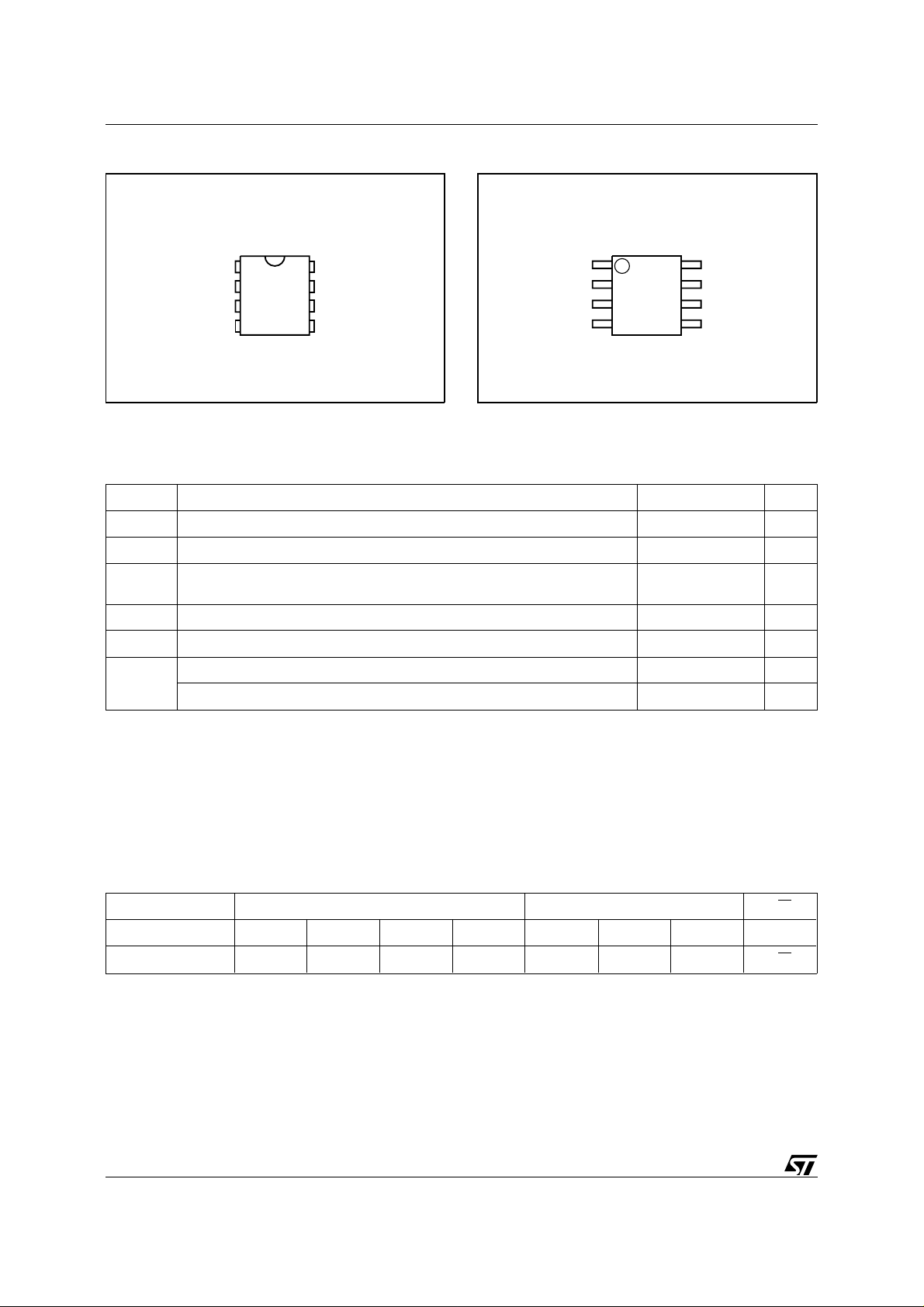
PSDIP8 (B)
0.25mm Frame
Figure 1. Logic Diag ra m
ST24LC21
NOT FOR NEW DESIGN
8
1
SO8 (M)
DESCRIP TION
The ST24LC21 is a 1K bit electrically erasable
programmable memory (EEPROM), organized by
8 bits.This device can operate in two modes: T ransmit Only mode and I
2
C bidirectional mode. When
powered, the device is i n Transmit Only mode with
EEPROM data clock ed out from the ris ing edge of
the signal applied on VCLK.
The device will switch to the I2C bidirectional m ode
upon the falling edge of the signal applied on SCL
pin. The ST24LC21 cannot switch from the I
2
bidirectional mode to the Tr ansmit Only m ode (except when the power supply is removed). The
device operates with a power supply value as low
as 2.5V . Bot h Plastic Dual-in-Line and Plastic Sm all
Outline packages are available.
T able 1. Signal Names
SDA Serial Data Address Input/Output
2
SCL Serial Clock (I
V
CC
V
SS
Supply Voltage
Ground
C mode)
V
CC
C
SCL
VCLK
ST24LC21
V
SS
SDA
AI01489
VCLK Clock Transmit only mode
June 1997 1/18
This is information on a product still in production but not recommended for new designs.
Page 2
ST24LC21
Figure 2A. DIP Pin Connect io ns
ST24LC21
1
NC V
2
3
NC
4
SS
8
7
6
5
AI01499
VCLKNC
SCL
SDAV
CC
Figure 2B. SO Pin Connecti ons
ST24LC21
NC V
1
2
NC
SS
3
4
8
7
6
5
AI01500
CC
VCLKNC
SCL
SDAV
Warning: NC = Not Connected Warning: NC = Not Connected
T ab le 2. Absolut e Maximu m Ra t ings
(1)
Symbol Parameter Value Unit
T
T
T
STG
LEAD
Ambient Operating Temperature grade 1 0 to 70 °C
A
Storage Temperature –65 to 150 °C
Lead Temperature, Soldering (SO8 package)
(PSDIP8 package)
40 sec
10 sec
215
260
°C
V
V
V
ESD
Notes: 1. Except for the rating "Operating Temperature Range", stresses above those listed in the Table "Absolute Maxim um Ratings"
Input or Output Voltages –0.3 to 6.5 V
IO
Supply Voltage –0.3 to 6.5 V
CC
Electrostatic Discharge Voltage (Human Body model)
Electrostatic Discharge Voltage (Machine model)
may cause permanent damage to the device. These are stress ratings only and operation of the device at these or any other
conditions above those indicat ed in the Operati ng sections of this specific ati on is not implied. Expos ure to Absolut e Maximum
Rating conditions for extended periods may affect device rel i abi lity. Refer also to the SGS-THOMSON SURE Program and other
relevant quality documents.
2. MIL-STD-883C, 3015.7 (100pF, 1500 Ω).
3. EIAJ IC-121 (Condition C) (200pF, 0 Ω).
(2)
(3)
4000 V
500 V
T ab le 3. Device Select Co de
Device Code Chip Enable RW
Bit b7 b6 b5 b4 b3 b2 b1 b0
Device Select 1 0 1 0 X X X R
Note: The MSB b7 is sent first.
X = 0 or 1.
W
2/18
Page 3
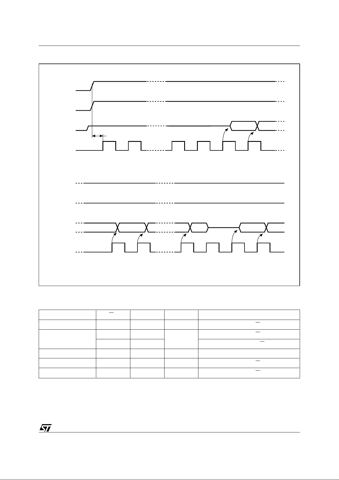
Figure 3. Transmi t Only Mode W avefo rms
V
CC
SCL
ST24LC21
SDA
VCLK
V
CC
SCL
SDA
VCLK
Bit 7
tVPU
12 891011
Bit 6 Bit 4 Bit 0
Bit 5
12 13 17 18 19 20
Bit 7
Bit 6
Bit 6
AI01501
T ab le 4. Operating Modes
Mode RW bit VCLK Bytes Initial Sequence
Current Address Read ’1’ X 1 START, Device Select, R
Random Address Read
’0’ X
1
START, Device Select, R
’1’ X reSTART, Device Select, R
Sequential Read ’1’ X 1 to 128 Similar to Current or Random Mode
Byte Write ’0’ V
Page Write ’0’ V
Note: X = VIH or V
IL
IH
IH
1 START, Device Select, RW = ’0’
8 START, Device Select, RW = ’0’
W = ’1’
W = ’0’, Address,
W = ’1’
3/18
Page 4
ST24LC21
Figure 4. Transit ion Mode W avefo rm s
SCL
SDA
VCLK
Bi-Directional ModeTransmit Only Mode
AI01502
Transmit Only Mode
After a Power-up, the device is in the Transmit O nly
mode. A proper initialization sequence must supply
nine clock pulses on the VCLK pin (in order to
internally synchronize the device). During this initialization sequence, the S DA pin is in high im pedance. On the rising edge of the tenth pulse applied
on VCLK pin, the device will output the first bit of
byte located at address 00h (most significant bit
first).
A byte is clocked out (on SDA pin) with nine clock
pulses on VCLK: 8 clock pulses for the data byte
and one extra clock pulse for a Don’t Care bit.
As long as the SCL pin is held high, each byte of
the memory arr ay is transmitted s erially on the SDA
pin with an automatic address increment.
When the last byte is transmitted, the address
counter will roll-over to location 00h.
2
C Bidirectional Mode
I
The device can be switched from Transmit Only
mode to I2C Bidirectional mode by applying a valid
high to low transition on the SCL pin (see Figure 4).
When the device is in the I2C Bidirectional mode,
the VCLK input enables (or inhibits) the executio n
of any write instruction: if VCLK = 1, write instructions are executed; if VCLK = 0, write instructions
are not executed.
2
The device is compatible wit h the I
C standard, two
wire serial interfac e which uses a bi-directional dat a
bus and serial clock. The device carries a built-in 4
bit, unique device identification code (1010) corresponding to the I
The device behaves as a slave device in the I
2
C bus definition.
2
protocol with all memory operations synchronized
by the serial clock. Read and write operations are
initiated by a START condition generated by the
bus master. The START condition is followed by a
stream of 7 bits (identification code 1010XX X), plus
one read/write bit and terminated by an acknowledge bit.
When writing data to the memory it responds to the
8 bits received by asserting an acknowledge bit
during the 9th bit time. When data is read by the
bus master, it acknowledges the receipt of the data
bytes in the same way. Data transfers are terminated with a STOP condition.
Power On Reset: V
lock out write protect. In
CC
order to prevent data corruption and inadvertent
write operations during power up, a Power On
Reset (POR) circuit is implemented. Until the V
CC
voltage has reached the POR thres hold value, t he
internal reset is active, all operations are disabled
and the device will not respond to any command.
In the same way, when V
drops down from the
CC
operating voltage to below the POR threshold
value, all operations are disabled and the device
will not respond to any command. A stable V
CC
must be applied before applying any logic signal.
C
4/18
Page 5
ST24LC21
SIGNAL DESCRIPTIONS
2
I
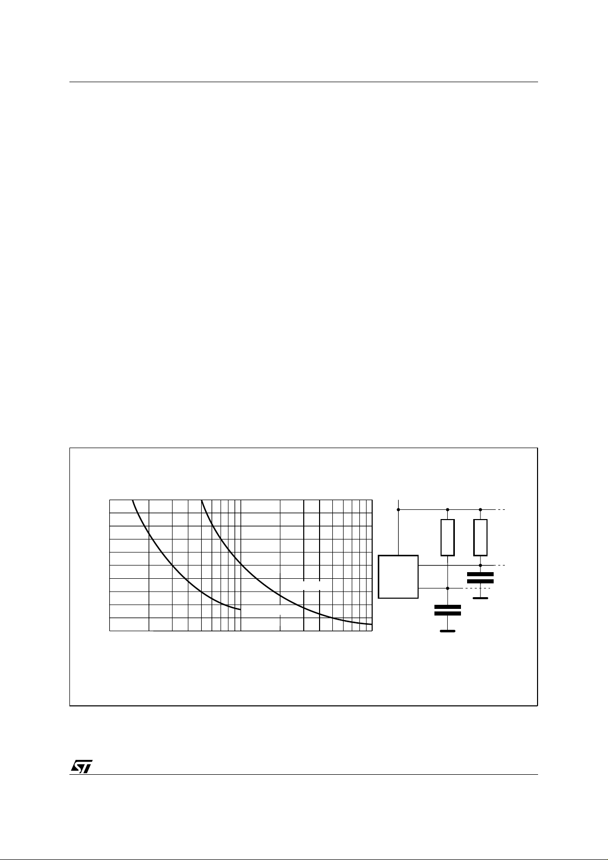
C Serial Clock (SCL ). The SCL input pin is used
to synchronize all data in and out of the memory . A
resistor can be connected from the SCL line to V
CC
to act as a pull up (see Figure 5).
Tr ansmit Only C lock (VCLK). The VCLK input pin
is used to synchronize data out when the
ST24LC21 is in Transmit Only mode. The VCLK
input offers also a Write Enable (active high) function when the ST24LC21 is in I
2
C bidirectional
mode.
Serial Data (SDA). The SDA pin is bi-directional
and is used to transfer data in or out of the memory .
It is an open drain output that may be wire-OR’ed
with other open drain or open collector signals on
the bus. A resistor must be connected from the SDA
bus line to V
to act as pull up (see Figure 5).
CC
DEVICE OPER ATION
2
I
C Bus Background
The ST24LC21 supports the I
2
C protocol. This
protocol defines any device that sends data onto
the bus as a transmitter and any device t hat reads
the data as a receiver . The device that c ontrols th e
data transfer is known as the master and the other
as the slave. The master will alway s initiate a dat a
transfer and will provide the serial clock for synchronisation. The ST24LC21 are always slave d evices in all communications.
Start Condition. START is identified by a high to
low transition of the SDA line while the clock SCL
is stable in the high state. A START condit ion must
precede any command for data transfer. Except
during a programming cycle, the ST24LC21 continuously monitor the SDA and SCL signals for a
START condition and will not respond unless one
is given.
Stop Condition. STOP is identified by a low to high
transition of the SDA line while the clock SCL is
stable in the high state. A STOP condition terminates communication between the ST24LC21 a nd
the bus master. A STOP condition at the end of a
Read command forces the standby stat e. A STO P
condition at the end of a Write command triggers
the internal EEPROM write cycle.
Acknowledge Bit (ACK). An acknowledge signal
is used to indicate a successfull data transfer. The
bus transmitter , either master or slave, will re lease
the SDA bus after sending 8 bits of data. During the
9th clock pulse period the receiver pulls the SDA
bus low to acknowledge the receipt of the 8 bits of
data.
Figure 5. Maximum RL Value versus Bus Capacitance (C
20
16
12
8
Maximum RP value (kΩ)
4
0
10 1000
C
BUS
fc = 400kHz
100
(pF)
fc = 100kHz
) for an I2C Bus
BUS
V
MASTER
CC
SDA
SCL
R
R
C
BUS
L
C
BUS
AI01665
L
5/18
Page 6
ST24LC21
T able 5. Input Parameters
(1)
(TA = 25 °C, f = 100 kHz )
Symbol Parameter Test Condition Min Max Unit
C
IN
C
IN
t
LP
Note: 1. Sampled only, n ot 100% tested.
Input Capacitance (SDA) 8 pF
Input Capacitance (other pins) 6 pF
Low-pass filter input time constant
(SDA and SCL)
300 ns
T ab le 6. DC Characteristics
= 0 to 70 °C; VCC = 2.5V to 5.5V)
(T
A
Symbol Parameter Test Condition Min Max Unit
I
I
I
LI
I
LO
CC
CC1
Input Leakage Current 0V ≤ VIN ≤ V
Output Leakage Current
Supply Current
Supply Current V
Supply Current (Standby)
0V ≤ V
V
= 5V, fC = 400kHz
CC
(Rise/Fall time < 10ns)
= 2.5V, fC = 400kHz 1 mA
CC
V
IN
V
IN
= 5V, fC = 400kHz
V
CC
≤ VCC
OUT
SDA in Hi-Z
= VSS or VCC,
= 5V
V
CC
= VSS or VCC,
CC
±2 µA
±2 µA
2mA
100 µA
300 µA
I
V
V
V
CC2
V
V
OL
V
= VSS or VCC,
IN
V
= 2.5V
Supply Current (Standby)
V
IL
IH
IL
IH
Input Low Voltage (SCL, SDA) –0.3 0.3 V
Input High Voltage (SCL, SDA) 0.7 V
Input Low Voltage (VCLK)
Input High Voltage (VCLK) 2 VCC + 1 V
Output Low Voltage
CC
V
= VSS or VCC,
IN
= 2.5V, fC = 400kHz
CC
CC
2.5V ≤ VCC ≤ 4V –0.3 0.2 V
V
> 4V –0.3 0.8 V
CC
IOL = 3mA 0.4 V
I
= 6mA, VCC = 5V 0.6 V
OL
5 µA
50 µA
CC
VCC + 1 V
CC
V
V
6/18
Page 7

ST24LC21
T ab le 7. AC Characteristics, I2C Bidirectional Mode for Clock Frequency = 400kHz
= 0 to 70 °C; VCC = 2.5V to 5.5V)
(T
A
Symbol Alt Parameter Min Max Unit
t
t
t
Notes: 1. Sampled only , not 100% teste d.
(1)
CH1CH2
(1)
CL1CL2
(1)
DH1DH2
(1)
t
DL1DL2
(2)
t
CHDX
t
CHCL
t
DLCL
t
CLDX
t
CLCH
t
DXCX
t
CHDH
t
DHDL
t
CLQV
t
CLQX
f
C
t
tWRWrite Time 10 ms
W
2. For a reSTART condition, or following a write cycle.
t
t
t
t
t
SU:STA
t
HIGH
t
HD:STA
t
HD:DAT
t
LOW
t
SU:DAT
t
SU:STO
t
BUF
t
AA
t
DH
f
SCL
R
F
R
F
Clock Rise Time 300 ns
Clock Fall Time 300 ns
SDA Rise Time 20 300 ns
SDA Fall Time 20 300 ns
Clock High to Input Transition 600 ns
Clock Pulse Width High 600 ns
Input Low to Clock Low (START) 600 ns
Clock Low to Input Transition 0 µs
Clock Pulse Width Low 1.3 µs
Input Transition to Clock Transition 100 ns
Clock High to Input High (STOP) 600 ns
Input High to Input Low (Bus Free) 1.3 µs
Clock Low to Data Out Valid 200 900 ns
Clock Low to Data Out Transition 200 ns
Clock Frequency 400 kHz
Data Input. During data input the ST 24LC21 sample the SDA bus signal on the rising edge of the
clock SCL. Note that for correct device operation
the SDA signal must be stable during the clock low
to high transition and the data must change ONLY
when the SCL line is low .
Memory Addressi ng. To start communic ation b etween the bus master and the slave ST24LC21, the
master must initiate a START condition. Following
this, the master sends onto the SDA bus line 8 bits
(MSB first) corresponding to the device select c ode
(7 bits) and a READ or WRITE bit. The 4 most
significant bits of the device select code are the
device type identifier , corresponding to the I
2
C bus
definition. For these memories the 4 bits are fixed
as 1010b. The f ollowing 3 bits are Don’t Care. The
8th bit sent is the read or write bit (R
W), this bit is
set to ’1’ for read and ’0’ for write operations. If a
match is found, the corresponding memory will
acknowledge the identification on the SDA bus
during the 9th bit time.
Write Operation s
Following a START condition the master sends a
device select code with the R
W bit r eset t o ’0’. Th e
memory acknowledges this and waits for a byte
address. After receipt of the byte address the device again responds with an acknowledge.
2
C bidirectional mode, any write command with
In I
VCLK = 0 will not modify data and will be acknowledged on data bytes, as shown in Figure 11.
Byte Write. In the Byte Write mode the master
sends one data byte, which is ac knowledged by the
memory. The master then terminates the transfer
by generating a STOP condition.
Page Write. The Page Write mode allows up to 8
bytes to be written in a single writ e c ycle, provided
that they are all located in the same ’row’ in the
memory: that is the most significant memory address bits are the same. The master sends from
one up to 8 bytes of data, which are each acknowledged by the memory .
7/18
Page 8

ST24LC21
T ab le 8. AC Characteristics, I2C Bidirectional Mode for Clock Frequency = 100kHz
= 0 to 70 °C; VCC = 2.5V to 5.5V)
(T
A
Symbol Alt Parameter Min Max Unit
t
CH1CH2
t
CL1CL2
t
DH1DH2
t
DL1DL1
(1)
t
CHDX
t
CHCL
t
DLCL
t
CLDX
t
CLCH
t
DXCX
t
CHDH
t
DHDL
(2)
t
CLQV
t
CLQX
f
C
t
W
Notes: 1. For a reSTART condition, or following a write cycle.
2. The minimum value delays the falling/rising edge of SDA away from SCL = 1 in order to avoid unwanted START and/or STOP
conditions.
t
t
t
t
t
SU:STA
t
HIGH
t
HD:STA
t
HD:DAT
t
LOW
t
SU:DAT
t
SU:STO
t
BUF
t
AA
t
DH
f
SCL
t
WR
R
F
R
F
Clock Rise Time 1 µs
Clock Fall Time 300 ns
Input Rise Time 1 µs
Input Fall Time 300 ns
Clock High to Input Transition 4.7 µs
Clock Pulse Width High 4 µs
Input Low to Clock Low (START) 4 µs
Clock Low to Input Transition 0 µs
Clock Pulse Width Low 4.7 µs
Input Transition to Clock Transition 250 ns
Clock High to Input High (STOP) 4.7 µs
Input High to Input Low (Bus Free) 4.7 µs
Clock Low to Next Data Out Valid 0.3 3.5 µs
Data Out Hold Time 300 ns
Clock Frequency 100 kHz
Write Time 10 ms
T ab le 9. AC Characteristics, Transmit-o nly Mode
= 0 to 70 °C; VCC = 2.5V to 5.5V)
(T
A
Symbol Alt Parameter Min Max Unit
t
VCHQX
t
VCHVCL
t
VCLVCH
t
CLQZ
(1,2)
t
VPU
(2)
t
VH1VH2
(2)
t
VL1VL2
Notes: 1. Refer to Figure 3.
2. Sampled only , not 100% teste d.
8/18
t
VAA
t
VHIGH
t
VLOW
t
VHZ
t
t
Output Valid from VCLK 500 ns
VCLK High Time 600 ns
VCLK Low Time 1.3 µs
Mode Tansition Time 500 ns
Transmit-only Power-up Time 0 ns
R
F
VCLK Rise Time 1 µs
VCLK Fall Time 1 µs
Page 9

Figure 6. AC Waveforms
ST24LC21
SCL
SDA IN
SCL
SDA OUT
SCL
tCHCL
tDLCL
tCHDX
START
CONDITION
tCLQV tCLQX
tDHDL
tCLDX
SDA
INPUT
DATA VALID
DATA OUTPUT
SDA
CHANGE
tW
tCLCH
tDXCX
tCHDH
tDHDL
STOP &
BUS FREE
SDA IN
VCLK
SDA
SCL
tCHDH
STOP
CONDITION
WRITE CYCLE
tVCHVCL tVCLVCH
tVCHQX
tCHDX
START
CONDITION
tCLQZ
AI01503
9/18
Page 10

ST24LC21
AC MEASUREMENT CONDITIONS
Input Rise and Fall Times ≤ 50ns
Input Pulse Voltages SDA, SCL 0.2V
Input Pulse Voltages V
CLK
Input and Output Timing Ref. Voltages 0.3V
CC
0.4V to 2V
CC
Figure 8. I2C Bus Protocol
SCL
SDA
START
CONDITION
to 0.8V
to 0.7V
SDA
INPUT
CC
CC
Figure 7. AC Testi ng Inpu t Outp ut W avefo r ms
0.8V
CC
0.2V
CC
SDA
CHANGE
STOP
CONDITION
0.7V
0.3V
AI00825
CC
CC
SCL
SDA
SCL
SDA
START
CONDITION
1 23 789
MSB
1 23 789
MSB ACK
ACK
STOP
CONDITION
AI00792
10/18
Page 11

Figure 9. Write Cycle Poll ing usin g ACK
WRITE Cycle
in Progress
START Condition
DEVICE SELECT
with RW = 0
ACK
NO
Returned
ST24LC21
First byte of instruction
with RW = 0 already
decoded by ST24xxx
ReSTART
STOP
YES
Next
Operation is
Addressing the
Memory
WRITE Operation
DEVICE OPER ATION S (cont’d)
After each byte is transfered, the internal byte
address counter (3 least significant bits only) is
incremented. The transfer is terminated by the
master generating a S TOP condition. Care must be
taken to avoid address counter ’roll-over’ which
could result in data being overwritten. Note that, for
any write mode, the generation by the master of the
STOP condition starts the internal memory program cycle. A ll inputs are disabled until the completion of this cycle and the memory will not respond
to any request.
Minimizing System Delays by Polling On ACK.
During the internal write cycle, the memory disconnects itself from the bus in order to copy the data
from the internal latches to the memory cells. The
maximum value of the write time (t
) is given in the
W
YESNO
Send
Byte Address
Proceed
Proceed
Random Address
READ Operation
AI01099B
AC Characteristics table, since the typical time is
shorter, the time seen by the system may be reduced by an ACK polling sequence issued by the
master. The sequence is as follows:
– Initial condition: a Wr ite is in progress (see Figure
9).
– Step 1: the Master issues a START condition
followed by a Device Select byte (1st byte of the
new instruction).
– Step 2: if the memory is busy with the internal
write cycle, no ACK will be returned and the
master goes back to Step 1. If the memory has
terminated the internal write cycle, it will respond
with an ACK, indicating that the memory is ready
to receive the second part of the next instruction
(the first byte of this instruction was already sent
during Step 1).
11/18
Page 12

ST24LC21
Figure 10. Wr ite Mo d es Sequ en c e
VCLK
BYTE WRITE DEV SEL BYTE ADDR DATA IN
ACK ACK ACK
VCLK
PAGE WRITE
R/W
START
ACK
DEV SEL BYTE ADDR
R/W
START
ACK ACK
DATA IN N
STOP
ACK ACK
DATA IN 1 DATA IN 2
STOP
AI01504B
Read Operations
On delivery, the me mory content is set at all "1’s"
(or FFh).
Current Address Read. The memory has an internal byte address counter. Each time a byte is read,
this counter is incremented. For the Current Address Read mode, following a START condition,
the master sends a memory address with the R
W
bit set to ’1’. The memory acknowledges this and
outputs the byte addressed by the internal byte
address counter . This counter is then incremented.
The master does NOT acknowledge the byte out-
12/18
put, but terminates the transfer with a STOP condition.
Random Address Read. A dummy write is performed to load the address into the address
counter , see Figure 12. This is followed by anoth er
START condition from the master and the byte
address is repeated with the R
W bit set to ’1’. The
memory acknowledges this and outputs the byte
addressed. The master does NOT acknowledge
the byte output, but terminates the transfer with a
STOP condition.
Page 13

ST24LC21
Figure 11. Inhib ited W ri te w hen V
VCLK
CONTROL
BYTE WRITE
START
CONTROL
PAGE WRITE WORD ADD n
START
CLK
BYTE
BYTE
= 0
ACK ACK
WORD ADDR DATA
ACK
ACK
ACK
DATA n
ACK
STOP
DATA n + 1
ACKACK
DATA n + 7
STOP
AI01505
Sequential Read. T his mode can be initiated wit h
either a Current Address Read or a Random Address Read. However, in this case the master
DOES acknowledge the data byte output and the
memory continues to output the next byte in sequence. To terminate the stream of bytes, the
master must NOT acknowledge the last byte output, but MUST generate a STOP condition. The
output data is from consecutive byte addresses,
with the internal byte address counter automat-
ically incremented after each byte output. After a
count of the last memory address, the address
counter will ’roll- over’ and the memory will continue
to output data.
Acknowledg e in Read Mode. In all read modes
the ST24LC21 wait for an ack nowledge during the
9th bit time. If the mast er does not pull the SD A line
low during this time, the ST24LC21 terminate the
data transfer and switches to a standby state.
13/18
Page 14

ST24LC21
Figure 12. Read Modes Sequ en ce
CURRENT
ADDRESS
READ
RANDOM
ADDRESS
READ
SEQUENTIAL
CURRENT
READ
SEQUENTIAL
RANDOM
READ
ACK
DEV SEL DATA OUT
R/W
START
ACK
DEV SEL * BYTE ADDR
R/W
START
ACK ACK ACK NO ACK
DEV SEL DATA OUT 1
R/W
START
ACK ACK
DEV SEL * BYTE ADDR
NO ACK
STOP
ACK ACK
DEV SEL * DATA OUT
R/W
START
DEV SEL * DATA OUT 1
NO ACK
STOP
DATA OUT N
STOP
ACK ACK
R/W
START
ACK NO ACK
DATA OUT N
STOP
Note: * The 7 Most Significant bits of DEV SEL bytes of a Random Read (1st byte and 3rd byte) must be identical.
START
R/W
AI00794C
14/18
Page 15

ORDERI NG INFO RM ATION S CH EM E
Example: ST24LC21 M 1 TR
ST24LC21
Package
B PSDIP8
0.25mm Frame
MSO8
Temperature Range
1 0 to 70 °C
Option
TR Tape & Reel
Packing
Devices are shipped from the factory with the memory content set at all "1’s" (FFh).
For a list of available options (Pac kage, etc...) or for further inf ormation on any aspect of this device, please
contact the SGS-THO MS O N Sales Offic e nearest to you.
15/18
Page 16

ST24LC21
PSDIP8 - 8 pin Plastic Skinny DIP, 0.25mm lead frame
Symb
Typ Min Max Typ Min Max
A 3.90 5.90 0.154 0.232
A1 0.49 – 0.019 –
A2 3.30 5.30 0.130 0.209
B 0.36 0.56 0.014 0.022
B1 1.15 1.65 0.045 0.065
C 0.20 0.36 0.008 0.014
D 9.20 9.90 0.362 0.390
E 7.62 – – 0.300 – –
E1 6.00 6.70 0.236 0.264
e1 2.54 – – 0.100 – –
eA 7.80 – 0.307 –
eB 10.00 0.394
L 3.00 3.80 0.118 0.150
N8 8
PSDIP8
mm inches
Drawing is not to scale
16/18
A2
A1AL
B
e1
B1
D
N
C
eA
eB
E1 E
1
PSDIP-a
Page 17

SO8 - 8 lead Plastic Small Outline, 150 mils body width
ST24LC21
Symb
Typ Min Max Typ Min Max
A 1.35 1.75 0.053 0.069
A1 0.10 0.25 0.004 0.010
B 0.33 0.51 0.013 0.020
C 0.19 0.25 0.007 0.010
D 4.80 5.00 0.189 0.197
E 3.80 4.00 0.150 0.157
e 1.27 – – 0.050 – –
H 5.80 6.20 0.228 0.244
h 0.25 0.50 0.010 0.020
L 0.40 0.90 0.016 0.035
α 0° 8° 0° 8°
N8 8
CP 0.10 0.004
SO8
mm inches
Drawing is not to scale
B
SO-a
h x 45˚
A
C
e
CP
D
N
E
H
1
LA1 α
17/18
Page 18

ST24LC21
Information furnished is believed to be accurate and reliable. However, SGS-THOMSON Microelectronics assumes no responsibility for the
consequences of use of such information nor for any infringement of patents or other rights of third parties which may result from its use. No
license is granted by implication or otherwise under any patent or patent rights of SGS-THOMSON Microelectronics. Specificat ions mentioned
in this publication are subject to change without notice. This publication supersedes and replaces all information previously supplied.
SGS-THOMSON Microelectronics products are not authorized for use as critical components in life support devices or systems without express
written approval of SGS-THOMSON Microelectronics.
© 1997 SGS-THOMSON Microelectronics - All Rights Reserved
2
Purchase of I
2
C Patent. Rights to use these components in an I2C system, is granted provided that the system conforms to
I
Australia - Brazil - Canada - China - France - Germany - Hong Kong - Italy - Japan - Korea - Malaysia - Malta - Morocco - The Netherlands -
C Components by SGS-THOMSON Microelectronics, conveys a license under the Philips
2
C Standard Specifications as defined by Philips.
the I
SGS-THOMSON Microelectronics GROUP OF COMPANIES
Singapore - Spain - Sweden - Switzerland - Taiwan - Thailand - United Kingdom - U.S.A.
18/18
 Loading...