

Page 1
Features
■ 90 Mbps (max) data rate when driven by a
totem pole driver
■ 8 Mbps (max) data rate when driven by an
open drain pole driver
■ Bi-directional level translation without
direction control pin
■ Wide V
■ Wide V
■ Power down mode feature – when either
supply is off, all I/Os are in high impedance
■ Low quiescent current (max 24 µA)
■ Able to be driven by totem pole and open drain
drivers
■ 5.5 V tolerant enable pin
■ ESD performance on all pins: ±2 kV HBM
■ Small package and footprint
QFN16 (2.6 x 1.8 mm) package
voltage range of 1.65 to 3.6 V
L
voltage range of 1.80 to 5.5 V
CC
ST2349
4-bit dual supply level translator
without direction control pin
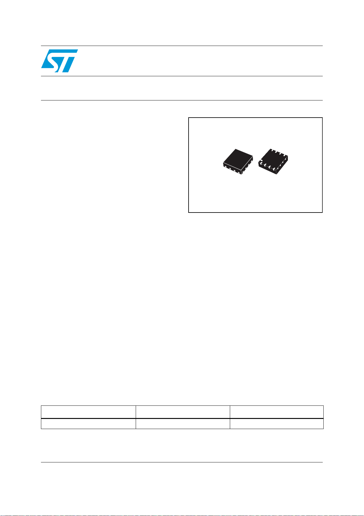
QFN16L
(2.6 x 1.8 mm)
Description
The ST2349 is a 4-bit dual supply level translator
which provides the level shifting capability to allow
data transfer in a multi-voltage system. Externally
applied voltages, V
on either side of the device. It utilizes
transmission gate-based design that allows bidirectional level translation without a control pin.
and VL, set the logic levels
CC
Applications
■ Low voltage system level translation
■ Mobile phones and other mobile devices
2
■ I
C level translation
■ UART level translation
The ST2349 accepts a V
V
from 1.80 to 5.5 V, making it ideal for data
CC
transfer between low-voltage ASICs/PLD and
higher voltage systems. This device has a tri-state
output mode which can be used to disable all
I/Os.
The ST2349 supports power down mode when
V
is grounded/floating and the device is
CC
from 1.65 to 3.6 V and
L
disabled via the OE pin.
Table 1. Device summary
Order code Package Packaging
ST2349QTR QFN16 (2.6 x 1.8 mm) Tape and reel (3000 parts per reel)
May 2008 Rev 4 1/23
www.st.com
23
Page 2

Contents ST2349
Contents
1 Pin settings . . . . . . . . . . . . . . . . . . . . . . . . . . . . . . . . . . . . . . . . . . . . . . . . 5
1.1 Pin connection . . . . . . . . . . . . . . . . . . . . . . . . . . . . . . . . . . . . . . . . . . . . . . 5
1.2 Pin description . . . . . . . . . . . . . . . . . . . . . . . . . . . . . . . . . . . . . . . . . . . . . . 5
2 Device block diagrams . . . . . . . . . . . . . . . . . . . . . . . . . . . . . . . . . . . . . . . 6
3 Supplementary notes . . . . . . . . . . . . . . . . . . . . . . . . . . . . . . . . . . . . . . . . 7
3.1 Driver requirement . . . . . . . . . . . . . . . . . . . . . . . . . . . . . . . . . . . . . . . . . . . 7
3.2 Load driving capability . . . . . . . . . . . . . . . . . . . . . . . . . . . . . . . . . . . . . . . . 7
3.3 Power off feature . . . . . . . . . . . . . . . . . . . . . . . . . . . . . . . . . . . . . . . . . . . . 7
3.4 Truth table . . . . . . . . . . . . . . . . . . . . . . . . . . . . . . . . . . . . . . . . . . . . . . . . . . 7
4 Maximum rating . . . . . . . . . . . . . . . . . . . . . . . . . . . . . . . . . . . . . . . . . . . . . 8
4.1 Recommended operating conditions . . . . . . . . . . . . . . . . . . . . . . . . . . . . . 8
5 Electrical characteristics . . . . . . . . . . . . . . . . . . . . . . . . . . . . . . . . . . . . . 9
5.1 AC characteristics (device driven by open drain driver) . . . . . . . . . . . . . . 11
5.2 AC characteristics (device driven by totem pole driver ) . . . . . . . . . . . . . 13
6 Waveforms . . . . . . . . . . . . . . . . . . . . . . . . . . . . . . . . . . . . . . . . . . . . . . . . 16
7 Package mechanical data . . . . . . . . . . . . . . . . . . . . . . . . . . . . . . . . . . . . 18
8 Revision history . . . . . . . . . . . . . . . . . . . . . . . . . . . . . . . . . . . . . . . . . . . 22
2/23
Page 3

ST2349 List of figures
List of figures
Figure 1. ST2349 pin connection (top through view) . . . . . . . . . . . . . . . . . . . . . . . . . . . . . . . . . . . . . 5
Figure 2. ST2349 block diagram . . . . . . . . . . . . . . . . . . . . . . . . . . . . . . . . . . . . . . . . . . . . . . . . . . . . . 6
Figure 3. Application block diagram . . . . . . . . . . . . . . . . . . . . . . . . . . . . . . . . . . . . . . . . . . . . . . . . . . . 6
Figure 4. Test circuit . . . . . . . . . . . . . . . . . . . . . . . . . . . . . . . . . . . . . . . . . . . . . . . . . . . . . . . . . . . . . 15
Figure 5. Waveform - propagation delay (f = 1 MHz; 50% duty cycle). . . . . . . . . . . . . . . . . . . . . . . . 16
Figure 6. Waveform - output enable and disable time (f = 1 MHz; 50% duty cycle) . . . . . . . . . . . . . 17
Figure 7. QFN16L (2.6 x 1.8 mm) package outline . . . . . . . . . . . . . . . . . . . . . . . . . . . . . . . . . . . . . . 18
Figure 8. QFN16L (2.6 x 1.8 mm) footprint recommendation . . . . . . . . . . . . . . . . . . . . . . . . . . . . . . 19
Figure 9. QFN16L (2.6 x 1.8 mm) carrier tape. . . . . . . . . . . . . . . . . . . . . . . . . . . . . . . . . . . . . . . . . . 20
Figure 10. QFN16L (2.6 x 1.8 mm) reel information . . . . . . . . . . . . . . . . . . . . . . . . . . . . . . . . . . . . . . 21
3/23
Page 4

List of tables ST2349
List of tables
Table 1. Device summary . . . . . . . . . . . . . . . . . . . . . . . . . . . . . . . . . . . . . . . . . . . . . . . . . . . . . . . . . . 1
Table 2. ST2349 pin description . . . . . . . . . . . . . . . . . . . . . . . . . . . . . . . . . . . . . . . . . . . . . . . . . . . . . 5
Table 3. Truth table. . . . . . . . . . . . . . . . . . . . . . . . . . . . . . . . . . . . . . . . . . . . . . . . . . . . . . . . . . . . . . . 7
Table 4. Absolute maximum ratings . . . . . . . . . . . . . . . . . . . . . . . . . . . . . . . . . . . . . . . . . . . . . . . . . . 8
Table 5. Recommended operating conditions . . . . . . . . . . . . . . . . . . . . . . . . . . . . . . . . . . . . . . . . . . 8
Table 6. DC characteristics (over recommended operating conditions unless otherwise noted. All typ-
ical values are at T
Table 7. AC characteristics - test conditions: V
tr = tf ≤ 2 ns) over temperature range -40 °C to 85 °C11
Table 8. AC characteristics - test conditions: V
tr = tf ≤ 2 ns) over temperature range -40 °C to 85 °C11
Table 9. AC characteristics - test conditions: V
tr = tf ≤ 2 ns) over temperature range -40 °C to 85 °C12
Table 10. AC characteristics (test conditions: V
tr = tf ≤ 2 ns) over temperature range -40 °C to 85 °C)13
Table 11. AC characteristics (test conditions: V
tr = tf ≤ 2 ns) over temperature range -40 °C to 85 °C)13
Table 12. AC characteristics (test conditions: V
tr = tf ≤ 2 ns) over temperature range -40 °C to 85 °C)14
Table 13. Test circuit switches . . . . . . . . . . . . . . . . . . . . . . . . . . . . . . . . . . . . . . . . . . . . . . . . . . . . . . 15
Table 14. Waveform symbol value . . . . . . . . . . . . . . . . . . . . . . . . . . . . . . . . . . . . . . . . . . . . . . . . . . . 16
Table 15. QFN16L (2.6 x 1.8 mm) mechanical data . . . . . . . . . . . . . . . . . . . . . . . . . . . . . . . . . . . . . . 19
Table 16. Document revision history . . . . . . . . . . . . . . . . . . . . . . . . . . . . . . . . . . . . . . . . . . . . . . . . . 22
= 25 oC)
A
= 1.65 - 1.8 V (load CL=15pF; Rup=4.7kΩ; driver
L
= 2.5 - 2.7 V (load CL=15pF; Rup=4.7kΩ; driver
L
= 2.7 - 3.6 V (load CL=15pF; Rup=4.7kΩ; driver
L
= 1.65 - 1.8 V (load CL=15pF; Rup=10kΩ; driver
L
= 2.5 - 2.7 V (load CL=15pF; Rup=10kΩ; driver
L
= 2.7 - 3.6 V (load CL=15pF; Rup=10kΩ; driver
L
4/23
Page 5
ST2349 Pin settings
1 Pin settings
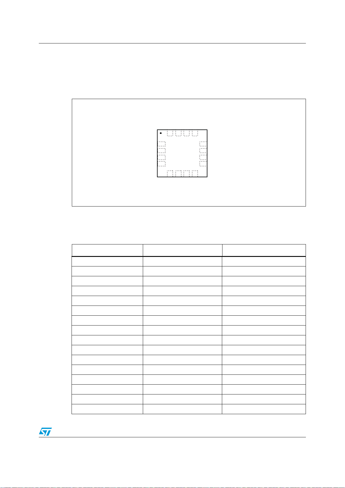
1.1 Pin connection
Figure 1. ST2349 pin connection (top through view)
1.2 Pin description
Table 2. ST2349 pin description
Pin number Symbol Name and function
1I/O
2 OE Output enable
3I/O
4I/O
5 NC No connection
6V
7V
8 NC No connection
9 I/O
10 I/O
11 GND Ground
I/O
I/O
I/O
VL2
OE
VL3
VL4
L
VL2
VL3
VL4
CC
VCC1
13 14 15 16
I/O
12
VCC2
11
GND
I/O
10
VCC3
9
O/I
VCC4
8
7
NC
CC
V
CS00022
Data input/output
Data input/output
Data input/output
L
Supply voltage
Supply voltage
Data input/output
Data input/output
VL1
I/O
VL VCC I/O
1
2
3
4
5
6
V
NC
VCC4
VCC3
12 I/O
13 I/O
14 V
15 V
16 I/O
5/23
VCC2
VCC1
CC
L
VL1
Data input/output
Data input/output
Supply voltage
Supply voltage
Data input/output
Page 6
Device block diagrams ST2349
2 Device block diagrams
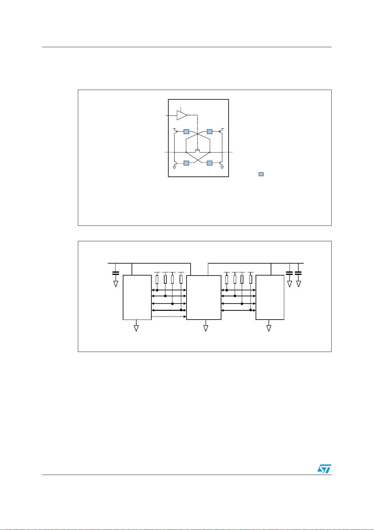
Figure 2. ST2349 block diagram
ST2349
VL
OE
I/O
VL
EN
VL
VCC
I/O
VCC
GND
* ST2349 has 4 channels. For simplicity, the above diagram shows only 1 channel.
* When OE is low, all I/Os are in high-impedance mode.
Figure 3. Application block diagram
V
L
0.1
μ
F
VL
system
controller
V
V
V
L VL
L
L
OE
I/O
I/O
I/O
I/O
GND
VCCVCCVCCV
V
V
L
CC
I/O
VL1
VCC1
I/O
VL2
VCC2
I/O
VL3
VCC3
I/O
VCC4
VL4
CC
= one-shot circuit
CC
V
system
controller
0.1 μF
1μF
CS00021
V
CD00023
CC
6/23
Page 7
ST2349 Supplementary notes
3 Supplementary notes
3.1 Driver requirement
The ST2349 may be driven by an open drain or totem pole driver and the nature of the
device’s output is “open drain”. It must not be used to drive a pull-down resistor since the
impedance of the output at HIGH state depends on the pull-up resistor placed at the I/Os.
As the device has pull-up resistors on both the I/O
ensure that the driver is able to sink the required amount of current. For example, if the
settings are V
=5.5V, VL= 4.3 V and the pull-up resistor is 10 kΩ, then the driver must be
CC
able to sink at least (5.5 V/10 kΩ) + (4.3 V/10 kΩ)
requirements of the ST2349.
3.2 Load driving capability
To support the open drain system, the one-shot transistor is turned on only during state
transition at the output side. When it drives a high state, after the one-shot transistor is
turned off, only the pull-up resistor is able to maintain the state. In this case, the resistive
load is not recommended.
During the translation from V
side to VL side, the oscillation might be triggered when the
CC
signal is reflected back as a glitch. This is caused by the architecture of the device (auto-
direction).
When using the ST2349, care need to be taken in the PCB data-track design and output
loading. It is recommended that the load is less than 25 pf.
3.3 Power off feature
In some applications where it might be required to turn off one of the power supplies
powering up the level translator, the user may turn off the V
(device is disabled). There will be no current consumption in V
other causes, and the I/Os are in a high-impedance state in this mode.
and I/OVL ports, the user needs to
VCC
= 1 mA and still meet the V
only when the OE pin is low
CC
due to floating gates or
L
IL
3.4 Truth table
Table 3. Truth table
Enable Bi-directional Input/Output
OE I/O
(1)
H
(1)
H
L Z
1. High level VL power supply referred
2. High level VCC power supply referred
3. Z = high impedance
VCC
(2)
H
L L
(3)
7/23
I/O
H
Z
(1)
(3)
VL
Page 8
Maximum rating ST2349
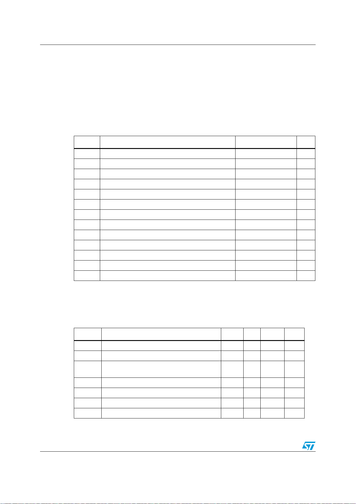
4 Maximum rating
Stressing the device above the rating listed in the “Absolute maximum ratings” table may
cause permanent damage to the device. These are stress ratings only, and operation of the
device at these or any other conditions above those indicated in the operating sections of
this specification is not implied. Exposure to absolute maximum rating conditions for
extended periods may affect device reliability. Refer also to the STMicroelectronics SURE
Program and other relevant quality documents.
Table 4. Absolute maximum ratings
Symbol Parameter Value Unit
V
Supply voltage -0.3 to 4.6 V
L
V
V
V
I/OVL
V
I/OVCC
I
I/OVL
I
I/OVCC
I
SCTOUT
P
T
ESD Electrostatic discharge protection (HBM) ±2 kV
Supply voltage -0.3 to 6.5 V
CC
DC control input voltage -0.3 to 6.5 V
OE
DC I/OVL input voltage (OE = GND or VL) -0.3 to VL + 0.3 V
DC I/O
DC input diode current -20 mA
I
IK
input voltage (OE = GND or VL) -0.3 to VCC + 0.3 V
VCC
DC output current ±25 mA
DC output current ±258 mA
Short circuit duration, continuous 40 mA
Power dissipation
D
Storage temperature -65 to 150
STG
(1)
500 mW
TL Lead temperature (10 seconds) 300
o
C
o
C
1. 500mW: 65oC derated to 300 mW by 10W/oC: 65oC to 85oC
4.1 Recommended operating conditions
Table 5. Recommended operating conditions
Symbol Parameter Min Typ Max Unit
V
V
CC
V
VI/O
VI/O
T
dt/dV Input rise and fall time (for 45 Mbps operation) 0 1 ns/V
1. VCC must be greater than VL.
8/23
Supply voltage 1.65 3.6 V
L
(1)
Supply voltage 1.8 5.5 V
Input voltage
OE
(OE output enable pin, VL power supply referred)
I/OVL voltage 0 V
VL
I/O
VCC
op
voltage 0 V
VCC
Operating temperature -40 85
03.6V
L
CC
V
V
o
C
Page 9
ST2349 Electrical characteristics
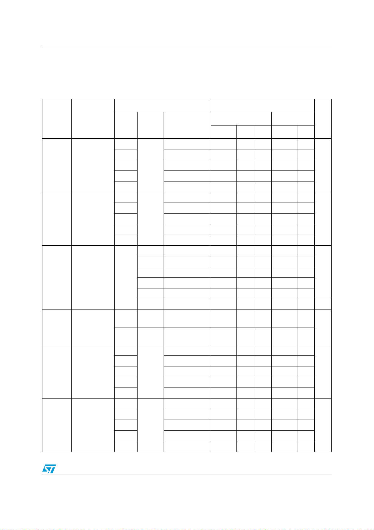
5 Electrical characteristics
Table 6. DC characteristics (over recommended operating conditions unless otherwise noted. All
typical values are at T
= 25 oC)
A
Test conditions Value
Symbol Parameter
TA = 25oC-40 to 85
V
L
V
CC
o
Unit
C
Min Typ Max Min Max
1.65
1.4 1.4
2.0 1.6 1.6
IHL
High level input
voltage (I/O
VL
V
L
to 5.5
2.5 2.0 2.0
)
V
V
3.0 2.4 2.4
3.6 2.8 2.8
1.65
0.3 0.3
2.0 0.4 0.4
ILL
Low level input
voltage (I/O
VL
V
2.5 0.5 0.5
)
V
L
to 5.5
V
3.0 0.6 0.6
3.6 0.8 0.8
1.8 1.6 1.6
2.5 2.3 2.3
High level input
IHC
voltage
(I/O
VCC
)
V
1.65 to
V
CC
3.0 2.7 2.7
3.6 3.3 3.3
V
4.3 3.5 3.5
V
V
V
ILC
IH-OE
IL-OE
Low level input
voltage
(I/O
)
VCC
High level input
voltage (OE)
Low level input
voltage (OE)
5.5 4.2 4.2
1.65 -
2.5
2.7 -
3.6
1.65
3 - 5.5 0.3
3.6 - 5.5 0.5
1.0 1.0
2.0 1.2 1.2
V
L
to 5.5
2.5 1.4 1.4
3.0 1.6 1.6
3.6 2.0 2.0
1.65
0.33 0.33
2.0 0.40 0.40
V
2.5 0.50 0.50
to 5.5
L
3.0 0.60 0.60
3.6 0.75 0.75
9/23
V
V
V
Page 10
Electrical characteristics ST2349
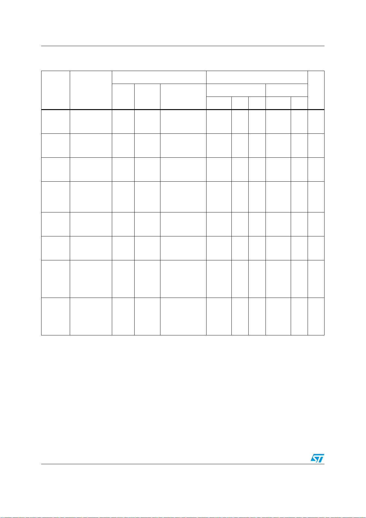
Table 6. DC characteristics (over recommended operating conditions unless otherwise noted. All
typical values are at T
= 25 oC) (continued)
A
Test conditions Value
Symbol Parameter
Low level
V
OLL
output voltage
)
(I/O
VL
Low level
V
OLC
output voltage
)
(I/O
VCC
Control input
I
OE
leakage current
(OE)
High
I
IO_LKG
impedance
leakage current
, I/O
(I/O
VL
VCC
Quiescent
I
QVCC
supply current
V
CC
Quiescent
I
QVL
supply current
V
L
High
impedance
I
Z-VCC
quiescent
supply current
V
CC
High
impedance
I
Z-VL
quiescent
supply current
V
L
)
V
L
1.65 to
3.6
1.65 to
3.6
1.65 to
3.6
1.65 to
3.6
1.65 to
3.6
1.65 to
3.6
1.65 to
3.6
1.65 to
3.6
TA = 25 oC-40 to 85 oC
V
CC
Min Typ Max Min Max
VL to 5.5
VL to 5.5
to 5.5
V
L
V
to 5.5 OE = GND ±0.1 ±0.1 µA
L
IO = 1.0 mA
I/O
≤ 0.15 V
VCC
IO = 1.0 mA
I/OVL ≤ 0.15 V
= GND or
V
OE
V
L
0.40 0.40 V
0.40 0.40 V
±0.1 ±0.1 µA
only pull-up
V
L
to 5.5
resistor
610 24µA
connected to I/O
only pull-up
V
L
to 5.5
resistor
0.01 0.1 1 µA
connected to I/O
OE = GND;
V
L
to 5.5
only pull-up
resistor
610 24µA
connected to I/O
OE = GND;
V
L
to 5.5
only pull-up
resistor
0.01 0.1 1 µA
connected to I/O
Unit
10/23
Page 11
ST2349 Electrical characteristics
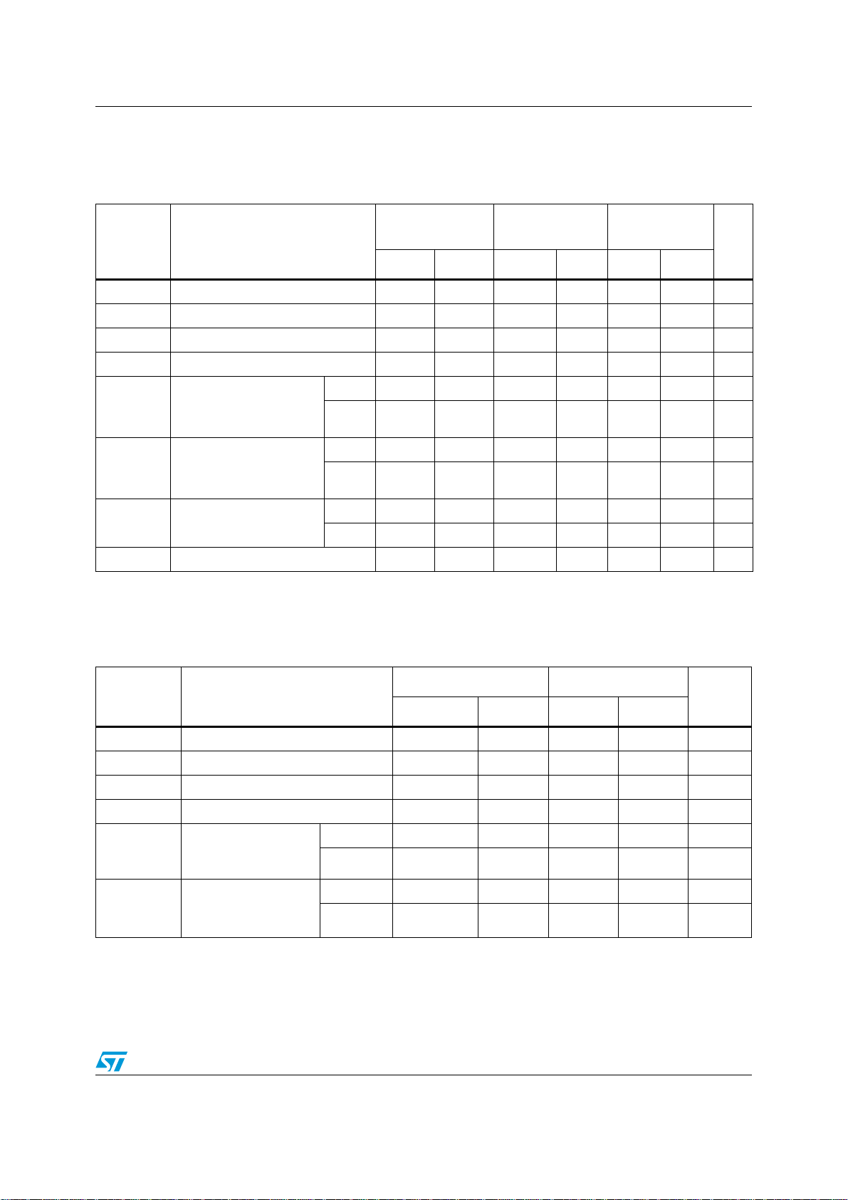
5.1 AC characteristics (device driven by open drain driver)
Table 7. AC characteristics - test conditions: VL = 1.65 −1.8 V (load CL=15pF; Rup=4.7kΩ;
Symbol Parameter
driver t
≤ 2 ns) over temperature range -40 °C to 85 °C
r=tf
V
=1.8−2.5 V VCC=2.7−3.6 V
CC
V
CC
=4.3−
5.5 V
Unit
Min Max Min Max Min Max
t
RVCC
t
FVCC
t
RVL
t
FVL
t
I/OVL-VCC
t
I/OVCC-VL
t
PZL tPZH
t
PLZ tPHZ
D
1. The data rate is guaranteed based on the condition that the output I/O signal rise/fall time is less than 15% of the input I/O
signal period; the input I/O signal is at 50% duty cycle and the output I/O signal duty cycle deviation not less than 30%.
Rise time I/O
Fall time I/O
Rise time I/O
Fall time I/O
Propagation delay time
I/O
VL-LH
I/O
VL-HL
Propagation delay time
I/O
VCC-LH
I/O
VCC-HL
Output enable and
disable time
Data rate
R
VCC
VL
to I/O
to I/O
to I/O
to I/O
(1)
VCC
VL
VCC-LH
VCC-HL
VL-LH
VL-LH
80 50 30 ns
333ns
766ns
455ns
t
PLH
t
PHL
t
PLH
t
PHL
555ns
555ns
555ns
577ns
En 10 10 10 ns
Dis 40 40 40 ns
1.6 2.5 4 MHz
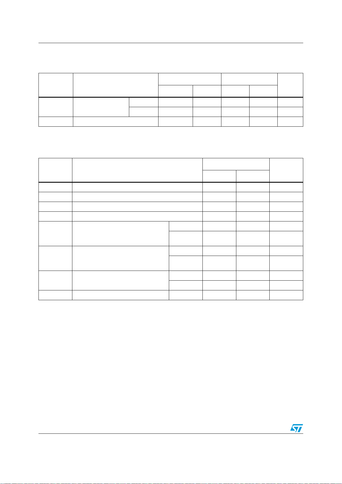
Table 8. AC characteristics - test conditions: VL=2.5−2.7 V (load CL=15pF; Rup=4.7kΩ; driver
t
≤ 2 ns) over temperature range -40 °C to 85 °C
r=tf
V
=2.7 −3.6 V VCC=4.3− 5.5 V
Symbol Parameter
t
RVCC
t
FVCC
t
RVL
t
FVL
Rise time I/O
Fall time I/O
Rise time I/O
Fall time I/O
VCC
VCC
VL
VL
Propagation delay time
t
I/OVL-VCC
I/O
I/O
VL-LH
VL-HL
to I/O
to I/O
VCC-LH
VCC-HL
Propagation delay time
t
I/OVCC-VL
I/O
VCC-LH
I/O
VCC-HL
to I/O
to I/O
VL-LH
VL-LH
t
PLH
t
PHL
t
PLH
t
PHL
CC
Unit
Min Max Min Max
70 40 ns
33ns
55ns
33ns
22ns
33ns
33ns
44ns
11/23
Page 12
Electrical characteristics ST2349
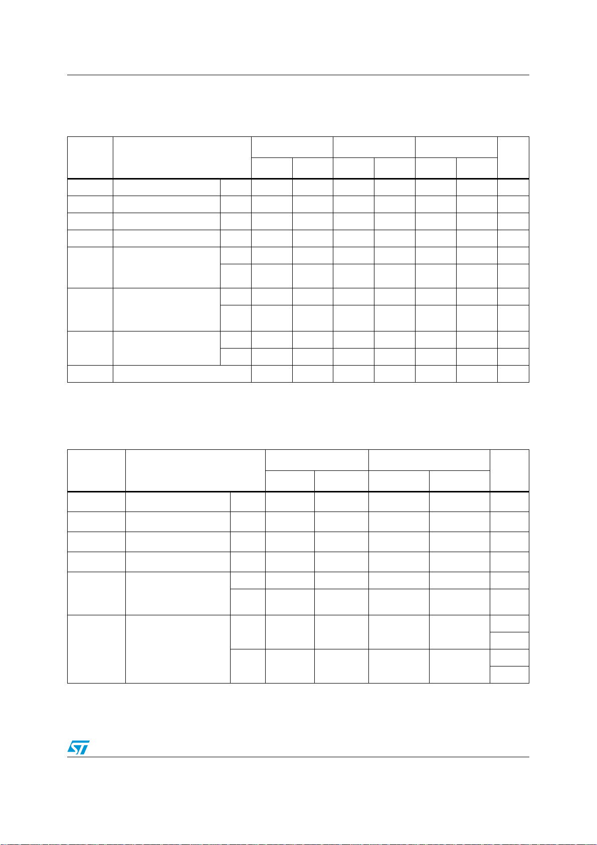
Table 8. AC characteristics - test conditions: VL=2.5−2.7 V (load CL=15pF; Rup=4.7kΩ; driver
t
≤ 2 ns) over temperature range -40 °C to 85 °C
r=tf
V
=2.7 −3.6 V VCC=4.3− 5.5 V
Symbol Parameter
CC
Unit
Min Max Min Max
t
PZL tPZH
t
PLZ tPHZ
D
R
1. The data rate is guaranteed based on the condition that the output I/O signal rise/fall time is less than 15% of the input I/O
signal period; the input I/O signal is at 50% duty cycle and the output I/O signal duty cycle deviation not less than 30%.
Output enable and
disable time
Data rate
(1)
En 6 6 ns
Dis 40 40 ns
2.5 3.2 MHz
Table 9. AC characteristics - test conditions: VL = 2.7 −3.6 V (load CL=15pF; Rup=4.7kΩ; driver
t
≤ 2 ns) over temperature range -40 °C to 85 °C
r=tf
V
= 4.3 − 5.5 V
Symbol Parameter
t
RVCC
t
FVCC
t
RVL
t
FVL
t
I/OVL-VCC
t
I/OVCC-VL
t
PZL tPZH
t
PLZ tPHZ
D
R
1. The data rate is guaranteed based on the condition that the output I/O signal rise/fall time is less than 15% of the input I/O
signal period; the input I/O signal is at 50% duty cycle and the output I/O signal duty cycle deviation not less than 30%.
Rise time I/O
Fall time I/O
Rise time I/O
Fall time I/O
VCC
VCC
VL
VL
Propagation delay time
VL-LH
VL-HL
to I/O
to I/O
VCC-LH
VCC-HL
I/O
I/O
Propagation delay time
I/O
VCC-LH
I/O
VCC-HL
to I/O
to I/O
VL-LH
VL-HL
Output enable and disable time
Data rate
(1)
t
PLH
t
PHL
t
PLH
t
PHL
En 6 ns
Dis 40 ns
CC
Unit
Min Max
55 ns
3ns
4ns
3ns
2ns
4ns
4ns
4ns
2.8 MHz
12/23
Page 13
ST2349 Electrical characteristics
5.2 AC characteristics (device driven by totem pole driver )
Table 10. AC characteristics (test conditions: VL=1.65– 1.8 V (load CL=15pF; Rup=10kΩ; driver
t
≤ 2 ns) over temperature range -40 °C to 85 °C)
r=tf
V
=1.8–2.5V VCC=2.7–3.6V VCC=4.3–5.5V
Symbol Parameter
CC
Unit
Min Max Min Max Min Max
t
RVCC
t
FVCC
t
RVL
t
FVL
t
I/OVL-
VCC
t
I/OVCC-
VL
t
PZL tPZH
t
PLZ tPHZ
D
1. The data rate is guaranteed based on the condition that the output I/O signal rise/fall time is less than 15% of the input I/O
signal period; the input I/O signal is at 50% duty cycle and the output I/O signal duty cycle deviation not less than 30%.
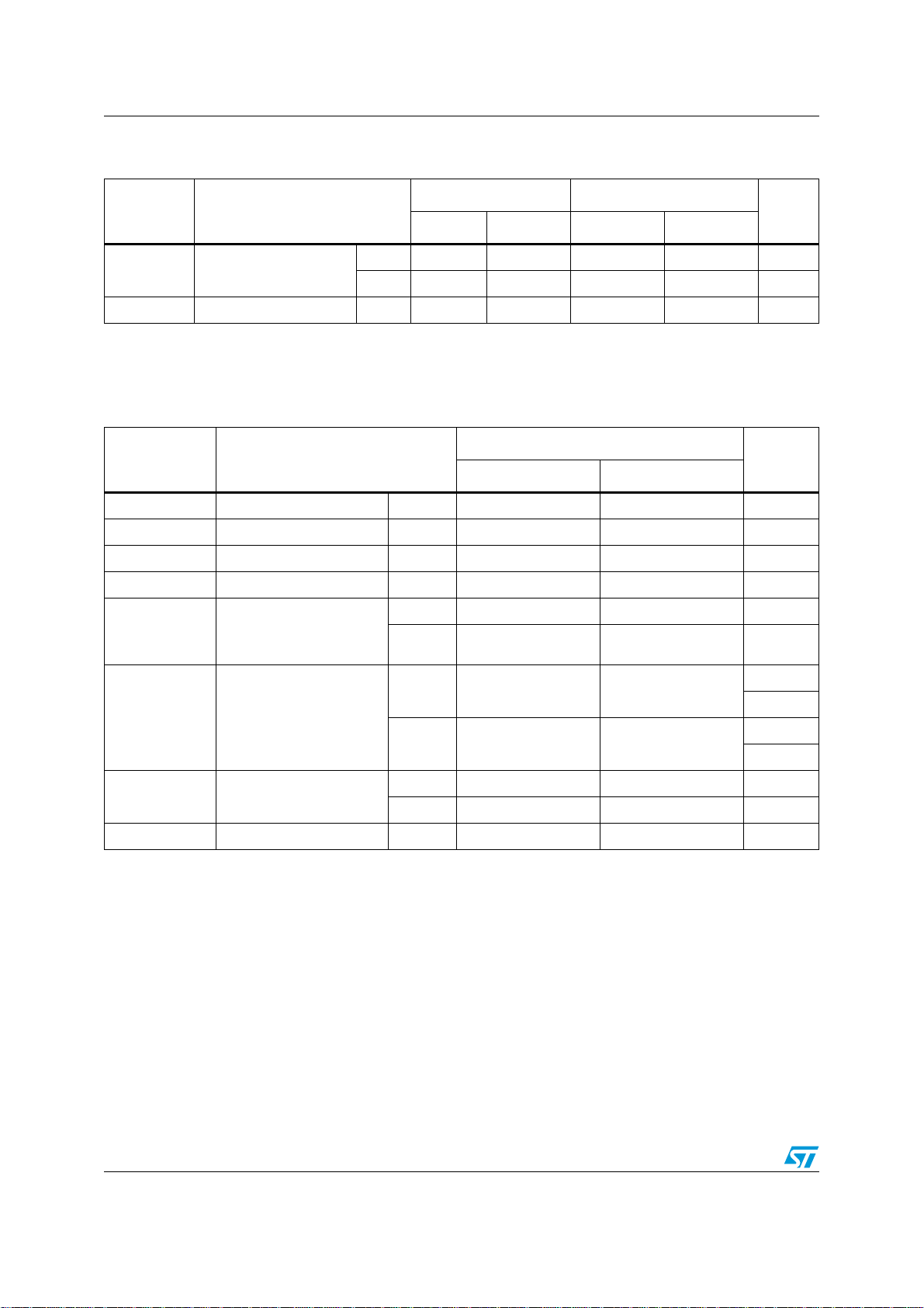
Table 11. AC characteristics (test conditions: VL=2.5– 2.7 V (load CL=15pF; Rup=10kΩ; driver
Rise time I/O
Fall time I/O
Rise time I/O
Fall time I/O
Propagation delay time
I/O
VL-LH
I/O
VL-HL
Propagation delay time
I/O
VCC-LH
I/O
VCC-HL
Output enable and
disable time
Data rate
R
t
≤ 2 ns) over temperature range -40 °C to 85 °C)
r=tf
VCC
VL
to I/O
to I/O
to I/O
to I/O
(1)
VCC
VL
VCC-LH
VCC-HL
VL-LH
VL-HL
t
PLH
t
PHL
t
PLH
t
PHL
En 10 10 10 ns
Dis 40 40 40 ns
Symbol Parameter
734ns
733ns
645ns
444ns
654ns
555ns
654ns
4.5 5.2 7 ns
12 32 32 MHz
V
=2.7 − 3.6 V VCC=4.3− 5.5 V
CC
Unit
Min Max Min Max
t
RVCC
t
FVCC
t
RVL
t
FVL
t
I/OVL-VCC
t
I/OVCC-VL
Rise time I/O
Fall time I/O
Rise time I/O
Fall time I/O
VCC
VCC
VL
VL
Propagation delay time
I/O
I/O
VL-LH
VL-HL
to I/O
to I/O
VCC-LH
VCC-HL
Propagation delay time
I/O
VCC-LH
I/O
VCC-HL
to I/O
to I/O
VL-LH
VL-HL
t
PLH
t
PHL
t
PLH
t
PHL
64ns
33ns
55ns
33ns
3.5 3 ns
44ns
ns
2.5 2.1
ns
ns
44
ns
13/23
Page 14
Electrical characteristics ST2349
Table 11. AC characteristics (test conditions: VL=2.5– 2.7 V (load CL=15pF; Rup=10kΩ; driver
t
≤ 2 ns) over temperature range -40 °C to 85 °C) (continued)
r=tf
V
=2.7 −3.6 V VCC=4.3−5.5 V
Symbol Parameter
CC
Unit
Min Max Min Max
t
PZL tPZH
t
PLZ tPHZ
D
R
1. The data rate is guaranteed based on the condition that the output I/O signal rise/fall time is less than 15% of the input I/O
signal period; the input I/O signal is at 50% duty cycle and the output I/O signal duty cycle deviation not less than 30%.
Table 12. AC characteristics (test conditions: VL=2.7– 3.6 V (load CL=15pF; Rup=10kΩ; driver
Output enable and
disable time
Data rate
t
r=tf
(1)
≤ 2 ns) over temperature range -40 °C to 85 °C)
Symbol Parameter
En 6 6 ns
Dis 40 40 ns
45 45 MHz
V
=4.3−5.5 V
CC
Unit
Min Max
t
RVCC
t
FVCC
t
RVL
t
FVL
t
I/OVL-VCC
Rise time I/O
Fall time I/O
Rise time I/O
Fall time I/O
VCC
VCC
VL
VL
Propagation delay time
VL-LH
VL-HL
to I/O
to I/O
VCC-LH
VCC-HL
I/O
I/O
t
t
PLH
PHL
5ns
3ns
4ns
3ns
2.5 ns
4ns
ns
t
Propagation delay time
(1)
to I/O
to I/O
VL-LH
VL-HL
t
I/OVCC-VL
t
PZL tPZH
t
PLZ tPHZ
D
R
1. The data rate is guaranteed based on the condition that the output I/O signal rise/fall time is less than 15% of the input I/O
signal period; the input I/O signal is at 50% duty cycle and the output I/O signal duty cycle deviation not less than 30%.
I/O
VCC-LH
I/O
VCC-HL
Output enable and disable
time
Data rate
PLH
t
PHL
En 6 ns
Dis 40 ns
2
ns
ns
4
ns
45 MHz
14/23
Page 15
ST2349 Electrical characteristics
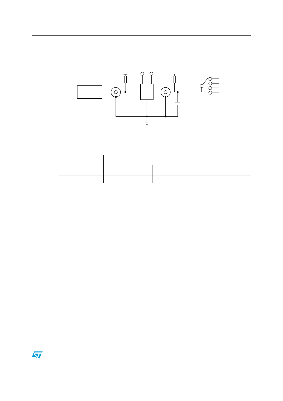
Figure 4. Test circuit
V
Pulse
generator
V
CC
V
L
R
up
L
D.U.T
V
CC
V
R
up
C
L
L
V
CC
OPEN
GND
Table 13. Test circuit switches
Test
Driving I/O
t
PLH
, t
PHL
Open Open Open
VL
Switch
Driving I/O
VCC
CS14021
Open drain driving
15/23
Page 16
Waveforms ST2349
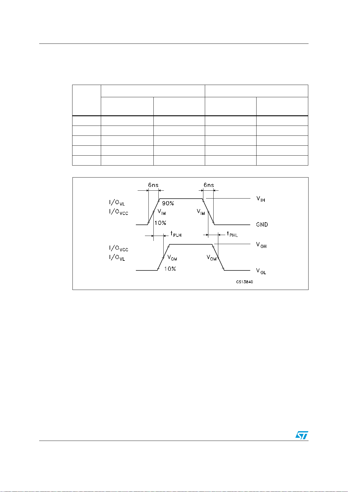
6 Waveforms
Table 14. Waveform symbol value
2.5 V
V
CC
50% V
Driving I/O
≤
CC
CC
L
Symbol
V
IH
V
IM
V
OM
V
X
V
Y
1.8 V ≤ VL≤ V
2.5 V
V
L
50% V
L
50% V
CC
Driving I/O
CC
VL
≤
3.3 V ≤ VL≤ V
5.0 V
V
50% V
50% V
≤
1.8 V ≤ VL≤ V
CC
L
L
CC
50% V
VOL +0.15V VOL +0.3V VOL +0.15V VOL +0.3V
VOH -0.15V VOH -0.3V VOH -0.15V VOH -0.3V
Figure 5. Waveform - propagation delay (f = 1 MHz; 50% duty cycle)
VCC
3.3V ≤ VL≤ V
5.0 V
V
CC
50% V
CC
50% V
≤
CC
L
16/23
Page 17
ST2349 Waveforms
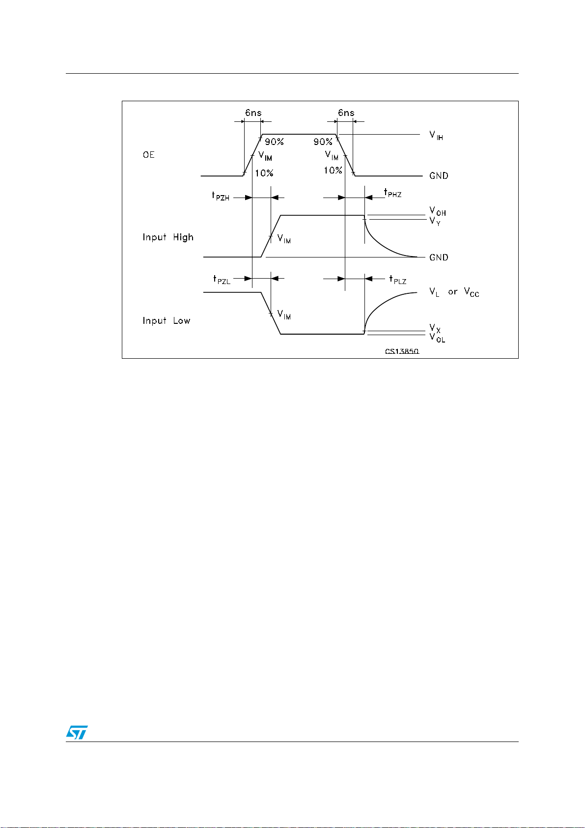
Figure 6. Waveform - output enable and disable time (f = 1 MHz; 50% duty cycle)
17/23
Page 18
Package mechanical data ST2349
7 Package mechanical data
In order to meet environmental requirements, ST offers these devices in ECOPACK®
packages. These packages have a Lead-free second level interconnect. The category of
second level interconnect is marked on the package and on the inner box label, in
compliance with JEDEC Standard JESD97. The maximum ratings related to soldering
conditions are also marked on the inner box label. ECOPACK is an ST trademark.
ECOPACK specifications are available at: www.st.com.
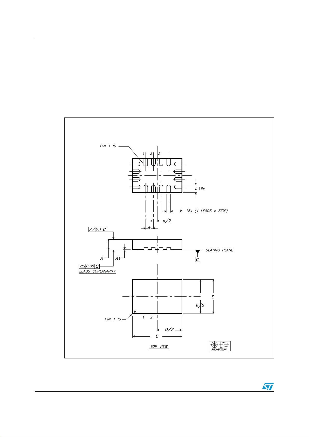
Figure 7. QFN16L (2.6 x 1.8 mm) package outline
BOTTOM VIEW
1. Drawing not to scale.
2. Dimensions are in millimeters.
18/23
QFN16L
Page 19
ST2349 Package mechanical data
Table 15. QFN16L (2.6 x 1.8 mm) mechanical data
Millimeters
Symbol
Typ Min Max
A 0.55 0.45 0.60
A1 0.02 0 0.05
b 0.20 0.15 0.25
D 2.60 2.50 2.70
E 1.80 1.70 1.90
e 0.40
L 0.40 0.35 0.45
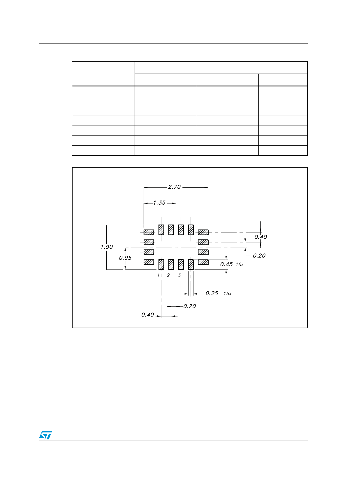
Figure 8. QFN16L (2.6 x 1.8 mm) footprint recommentations
1. Drawing not to scale.
2. Dimensions are in millimeters.
7874009
19/23
Page 20
Package mechanical data ST2349
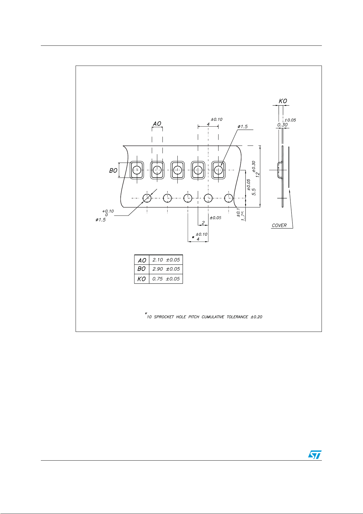
Figure 9. QFN16L (2.6 x 1.8 mm) carrier tape
20/23
785978-J
Page 21
ST2349 Package mechanical data
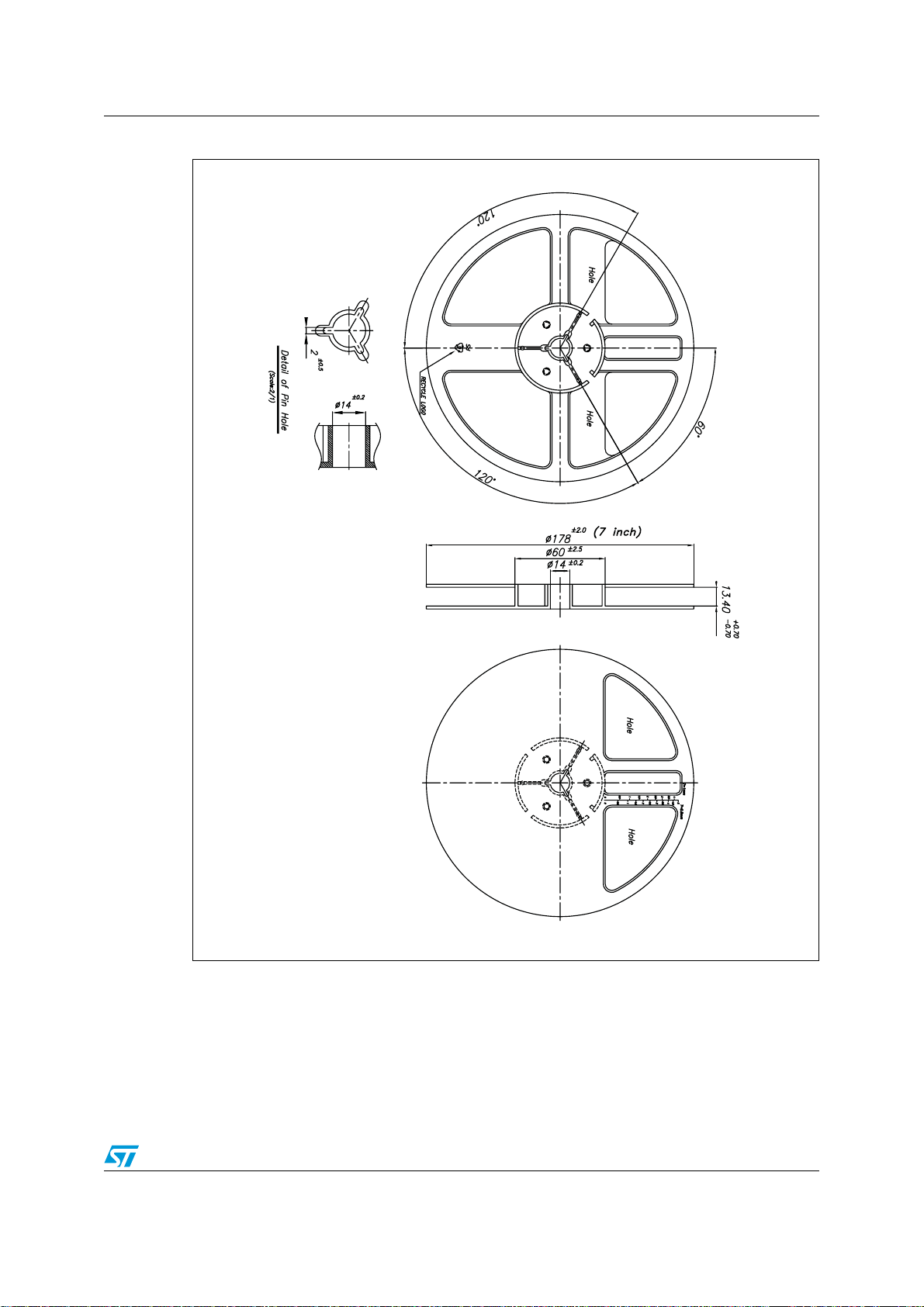
Figure 10. QFN16L (2.6 x 1.8 mm) reel information
1. Drawing not to scale.
2. Dimensions are in millimeters
7875978
21/23
Page 22
Revision history ST2349
8 Revision history
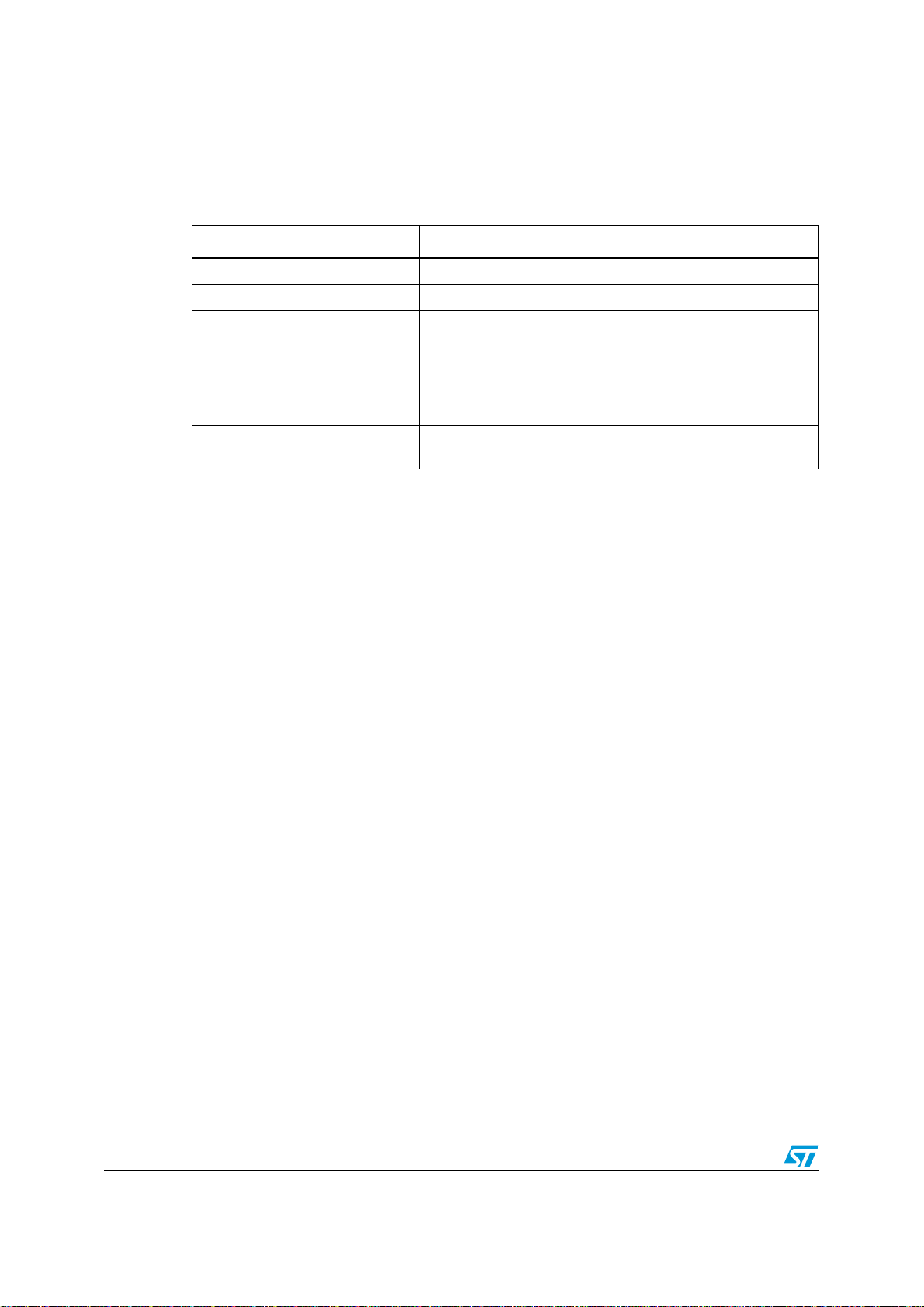
Table 16. Document revision history
Date Revision Changes
07-May-2007 1 Initial release.
29-May-2007 2 Typo in cover page title.
Removed Data Brief classification from the cover page.
Modified title and features section, added the following sections:
26-Nov-2007 3
07-May-2008 4
Section 1: Pin settings, Section 2: Device block diagrams,
Section 3: Supplementary notes, Section 4: Maximum rating,
Section 5: Electrical characteristicsSection 6: Waveforms and
updated Section 7: Package mechanical data.
Updated data rate values and added paragraph on load driving
capability (Section 3.2).
22/23
Page 23

ST2349
Please Read Carefully:
Information in this document is provided solely in connection with ST products. STMicroelectronics NV and its subsidiaries (“ST”) reserve the
right to make changes, corrections, modifications or improvements, to this document, and the products and services described herein at any
time, without notice.
All ST products are sold pursuant to ST’s terms and conditions of sale.
Purchasers are solely responsible for the choice, selection and use of the ST products and services described herein, and ST assumes no
liability whatsoever relating to the choice, selection or use of the ST products and services described herein.
No license, express or implied, by estoppel or otherwise, to any intellectual property rights is granted under this document. If any part of this
document refers to any third party products or services it shall not be deemed a license grant by ST for the use of such third party products
or services, or any intellectual property contained therein or considered as a warranty covering the use in any manner whatsoever of such
third party products or services or any intellectual property contained therein.
UNLESS OTHERWISE SET FORTH IN ST’S TERMS AND CONDITIONS OF SALE ST DISCLAIMS ANY EXPRESS OR IMPLIED
WARRANTY WITH RESPECT TO THE USE AND/OR SALE OF ST PRODUCTS INCLUDING WITHOUT LIMITATION IMPLIED
WARRANTIES OF MERCHANTABILITY, FITNESS FOR A PARTICULAR PURPOSE (AND THEIR EQUIVALENTS UNDER THE LAWS
OF ANY JURISDICTION), OR INFRINGEMENT OF ANY PATENT, COPYRIGHT OR OTHER INTELLECTUAL PROPERTY RIGHT.
UNLESS EXPRESSLY APPROVED IN WRITING BY AN AUTHORIZED ST REPRESENTATIVE, ST PRODUCTS ARE NOT
RECOMMENDED, AUTHORIZED OR WARRANTED FOR USE IN MILITARY, AIR CRAFT, SPACE, LIFE SAVING, OR LIFE SUSTAINING
APPLICATIONS, NOR IN PRODUCTS OR SYSTEMS WHERE FAILURE OR MALFUNCTION MAY RESULT IN PERSONAL INJURY,
DEATH, OR SEVERE PROPERTY OR ENVIRONMENTAL DAMAGE. ST PRODUCTS WHICH ARE NOT SPECIFIED AS "AUTOMOTIVE
GRADE" MAY ONLY BE USED IN AUTOMOTIVE APPLICATIONS AT USER’S OWN RISK.
Resale of ST products with provisions different from the statements and/or technical features set forth in this document shall immediately void
any warranty granted by ST for the ST product or service described herein and shall not create or extend in any manner whatsoever, any
liability of ST.
ST and the ST logo are trademarks or registered trademarks of ST in various countries.
Information in this document supersedes and replaces all information previously supplied.
The ST logo is a registered trademark of STMicroelectronics. All other names are the property of their respective owners.
© 2008 STMicroelectronics - All rights reserved
STMicroelectronics group of companies
Australia - Belgium - Brazil - Canada - China - Czech Republic - Finland - France - Germany - Hong Kong - India - Israel - Italy - Japan -
Malaysia - Malta - Morocco - Singapore - Spain - Sweden - Switzerland - United Kingdom - United States of America
www.st.com
23/23
 Loading...