

Page 1
ST232A
VERY HIGHSPEED,ULTRALOWPOWERCONSUMPTION
5V POWERED RS-232 DRIVERS AND RECEIVERS
■ SUPPLYVOLTAGERANGE:4.5TO 5.5V
■
SUPPLYCURRENTNO LOAD(TYP): 1.5mA
■ TRANSMITTEROUTPUTVOLTAGESWING
(TYP):±9V
■
TRANSITIONSLEWRATE (TYP.):12V/µs
■ RECEIVERPROPAGATIONDELAY
(TYP.):0.1µs
■ RECEIVERINPUTVOLTAGERANGE:
■ DATARATE(TYP):400Kbp/s
■
OPERATINGTEMPERATURERANGE:
-40TO 85
o
C,0 TO70oC
DESCRIPTION
The ST232A is a 2 driver, 2 receiver device
following EIA/TIA-232 and V.28 communication
standard. It is particularly suitable for applications
where±12V is not available. The ST232 uses a
single 5V power supply and only four external
capacitors (0.1µF). Typical applications are in:
Portable Computers, Low Power Modems,
Interfaces Translation, Battery Powered RS-232
System,Multi-Drop RS-232Networks.
±30V
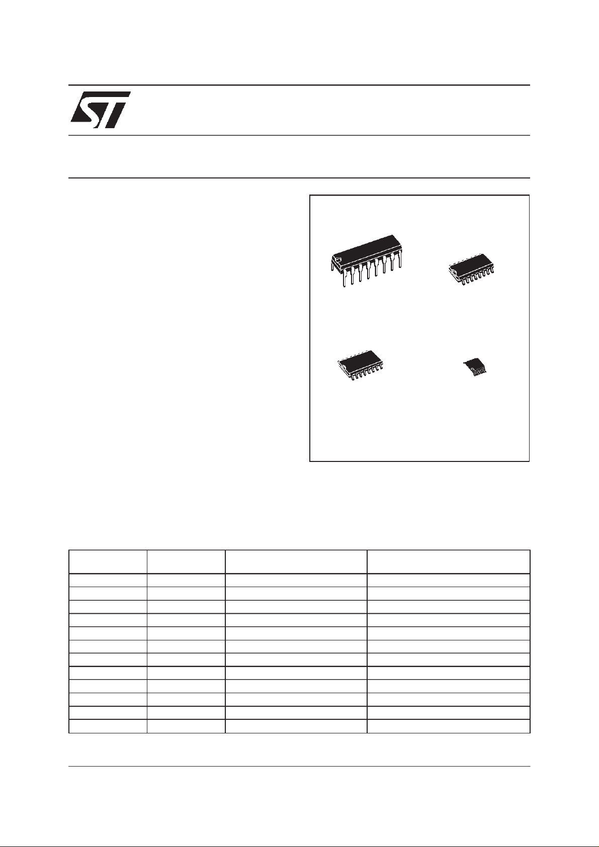
N
(PlasticPackage)
(Micro Package)
D
W
(Micro PackageLarge)T(TSSOPPackage)
ORDERCODES
Type Temperature
ST232ACN 0 to 70
ST232ABN -40 to 85
ST232ACD 0 to 70
ST232ABD -40 to 85
ST232ACDR 0 to 70
ST232ABDR -40 to 85
ST232ACW 0 to 70
ST232ABW -40 to 85
ST232ACWR 0 to 70
ST232ABWR -40 to 85
ST232ACTR 0 to 70
ST232ABTR -40 to 85
October 1999
Package Commen ts
Rang e
o
C DIP-16 25 parts per tube / 40 tubeper box
o
C DIP-16 25 parts per tube / 40 tubeper box
o
C SO-16 (Tube) 50 parts per tube / 20 tubeper box
o
C SO-16 (Tube) 50 parts per tube / 20 tube per box
o
C SO-16 (Tape & Reel) 2500 parts per reel
o
C SO-16 (Tape & Reel) 2500 parts per reel
o
C SO-16 Large (Tube) 50 parts per tube / 20 tubeper box
o
C SO-16 Large (Tube) 50 parts per tube / 20 tube per box
o
C SO-16 Large (Tape & Reel) 1000 parts per reel
o
C SO-16 Large (Tape & Reel) 1000 parts per reel
o
C TSSOP16 (Tape & Reel) 2500 parts per reel
o
C TSSOP16 (Tape & Reel) 2500 parts per reel
1/10
Page 2
ST232A
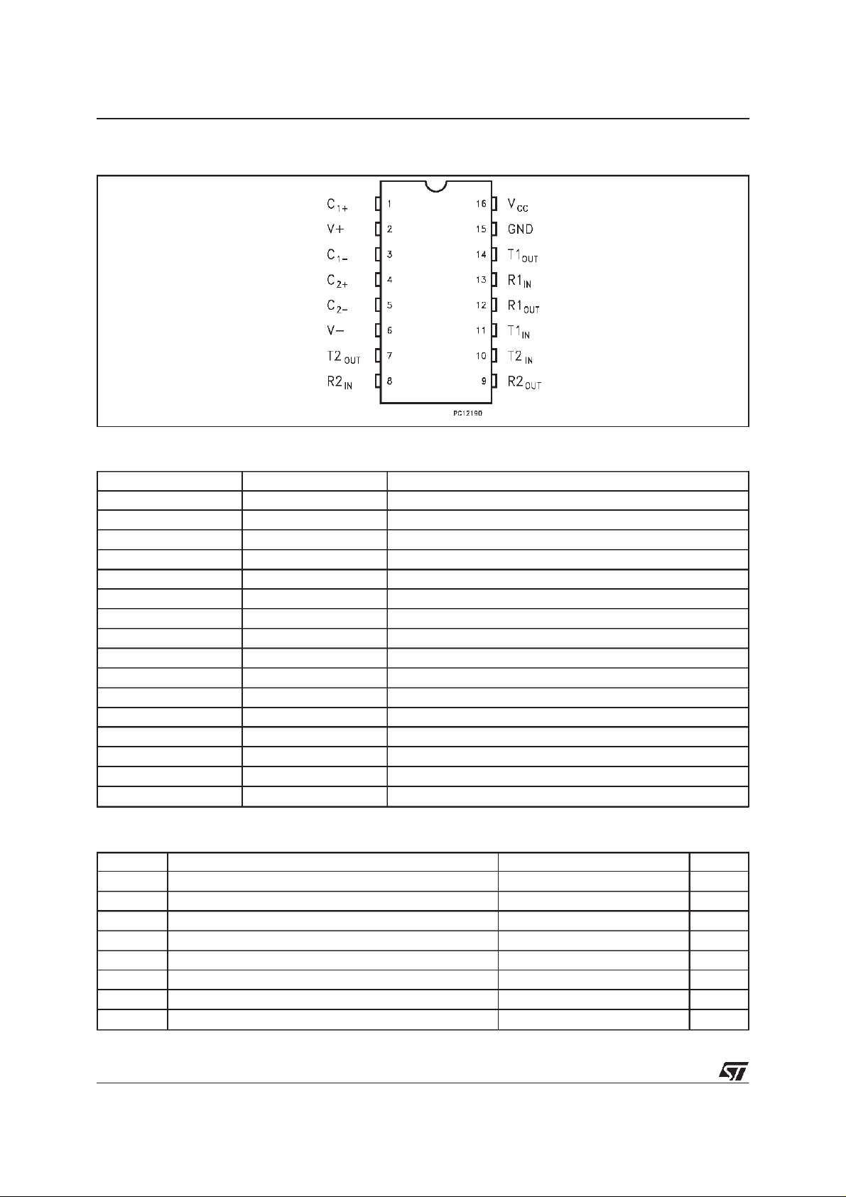
PIN CONFIGURATION
PIN DESCRIPTION
PIN No SYMBOL NAM E AND F UNC T I O N
1C
2 V+ Doubled Voltage Terminal
3C
4C
5C
6 V- Inverted Voltage Terminal
7T2
8R2
9R2
10 T2
11 T1
12 R1
13 R1
14 T1
15 GND Ground
16 V
+ Positive Terminal for the first Charge Pump Capacitor
1
- Negative Terminal for the first Charge Pump Capacitor
1
+ Positive Terminal for the second Charge Pump Capacitor
2
- Negative Terminal for the second Charge Pump Capacitor
2
OUT
IN
OUT
IN
IN
OUT
IN
OUT
CC
Second Transmitter Output Voltage
Second Receiver Input Voltage
Second Receiver Output Voltage
Second Transmitter Input Voltage
First Transmitter Input Voltage
First Receiver Output Voltage
First Receiver Input Voltage
First Transmitter Output Voltage
Supply Voltage
ABSOLUTE MAXIMUM RATINGS
Symb o l Para met er Val u e Uni t
V
V+ Extra Positive Voltage (V
V- Extra Negative Voltage 0.3 to -13.2 V
T
R
T
OUT
R
OUT
T
SCTOUT
AbsoluteMaximumRatingsarethosevaluesbeyondwhichdamagetothedevicemayoccur. Functionaloperationunderthese conditionisnot implied.
2/10
Supply Voltage -0.3 to 6 V
CC
-0.3)to 13.2 V
CC
Transmitter Input Voltage Range -0.3 to (VCC+ 0.3) V
IN
Receiver Input Voltage Range
IN
30 V
±
Transmitter Output Voltage Range ±15 V
Receiver Output Voltage Range -0.3 to (VCC+ 0.3) V
Short Circuit Duration on T
OUT
infinite
Page 3
ST232A
ELECTRICAL CHARACTERISTICS
(C
TypicalValus are referred to T
Symbol Parameter Test Conditions Value Unit
TRANSMITTER ELECTRICAL CHARACTERISTICS
(C
TypicalValus are referred to T
Symbol Parameter Test Conditions Value Unit
Note1:Measuredfrom3Vto -3Vor from-3V to3V.
Note2: One trasmitter output is loaded with R
= 0.1µF, VCC=5V±10% TA= -40 to 85oC, unless otherwise specified.
1-C4
=25oC)
A
I
SUPPLYVCC
1-C4
V
TOUT
Power Supply Current No Load 1.5 4 mA
= 0.1µF, VCC=5V±10%, TA= -40 to 85oC, unless otherwise specified.
=25oC)
A
Output Voltage Swing All Transmitter outputs are
loaded with 3KΩto GND
Logic Pull-Up Current TIN=0V 5 40
I
TIL
Input Logic Threshold Low 0.8 1.4 V
V
TIL
V
SR
R
Input Logic Threshold High 1.4 2 V
TIH
Transition Slew Rate TA=25oC, VCC=5V,
T
D
Data Rate (Note 2) 200 400 Kbits/s
R
Transmitter Output Resistance VCC= V+ = V- = 0V
TOUT
Transmitter Output Short Circuit
I
SC
=3to7KΩ,
R
L
= 50 to 2500 pF (Note 1)
C
L
=±2V
V
OUT
one T
to GND ±7 ±22 mA
XOUT
Current
Propagation Delay Time TTL-CMOS IN to RS-232 OUT
t
dT
=3KΩ to7KΩ,CL= 50to 1000pF
L
= 150 pF (50% to 50%)
C
L
Min. Typ. Max.
Min. Typ. Max.
±5 ±9V
µ
61230V/
300 10M Ω
1.3 3.5
µ
A
s
µ
s
RECEIVERELECTRICAL CHARACTERISTICS
(C
TypicalValus are referred to T
Symbol Parameter Test Conditions Value Unit
Note1:RS-232INtoTTL-CMOSOUT(from50% to50%)
= 0.1µF, VCC=5V±10%, TA= -40 to 85oC, unless otherwise specified.
1-C4
=25oC)
A
V
Receiver Input Voltage Operating
RIN
Range
R
V
V
V
V
V
I
RS-232 Input Resistance TA=25oC, 357K
RIN
RS-232 Input Logic Threshold Low 0.8 1.3 V
RIL
RS-232 Input Logic Threshold High 1.8 2.4 V
RIH
RS-232 Input Hysteresis VCC= 5 V 0.2 0.5 1 V
RIHYS
TTL/CMOS Output Voltage Low I
ROL
TTL/CMOS Output Voltage High I
ROH
Receiver Output Short Circuit
SCR
Current
Propagation Delay Time CL=150pF (Note 1) 0.1 0.5
t
dR
= 3.2mA (to VCC) 0.2 0.4 V
OUT
= 1mA (to GND) 3.5 VCC-0.2 V
OUT
to GND
to V
CC
Min. Typ. Max.
-30 30 V
2
10
10
30
mA
mA
µ
Ω
s
3/10
Page 4

ST232A
APPLICATION CIRCUITS
TTL / CMOS INPUTS
(note 1, note2)
C5
1
C1+
+
C1
3
C1-
4
C2+
+
C2
C2-
5
11
IN
10
T2
IN
+5V INPUT
+
+5VTO +10V
VOLTAGE
DOUBLER
+10VTO -10V
VOLTAGE
INVERTER
+5V
400K
+5V
400K
16
Vcc
T1
T2
C3
T1
T2
V+
V-
OUTT1
OUT
+
2
+10V
6
-10V
C4
+
14
RS 232OUTPUTS
7
TTL / CMOS OUTPUTS
Note1:C
Note2:C
capacitorscan even be1 µFones.
1-4
canbecommonorbiasedcapacitors.
1-4
CapacitanceValue (µF)
C1 C2 C3 C4 C5
0.1 0.1 0.1 0.1 0.1
12
9
OUT
R1
R2OUT
R1
R2
GND
15
R1IN
5K
R2
5K
13
RS 232INPUTS
IN
8
4/10
Page 5

ST232A
DriverVoltage Transfer Characteristics
DriverShort Circuit Output Currentvs
Temperature
DriverOutput Current vs OutputVoltage
DriverShort Circuit Supply Current vs
Temperature
ReceiverThresholdvs SupplyVoltage
ReceiverThresholdvs Temperature
5/10
Page 6

ST232A
Plastic DIP-16 (0.25) MECHANICAL DATA
DIM.
MIN. TYP. MAX. MIN. TYP. MAX.
a1 0.51 0.020
B 0.77 1.65 0.030 0.065
b 0.5 0.020
b1 0.25 0.010
D 20 0.787
E 8.5 0.335
e 2.54 0.100
e3 17.78 0.700
F 7.1 0.280
I 5.1 0.201
L 3.3 0.130
Z 1.27 0.050
mm inch
6/10
P001C
Page 7

SO-16 MECHANICAL DATA
ST232A
DIM.
MIN. TYP. MAX. MIN. TYP. MAX.
A 1.75 0.068
a1 0.1 0.2 0.004 0.007
a2 1.65 0.064
b 0.35 0.46 0.013 0.018
b1 0.19 0.25 0.007 0.010
C 0.5 0.019
c1 45 (typ.)
D 9.8 10 0.385 0.393
E 5.8 6.2 0.228 0.244
e 1.27 0.050
e3 8.89 0.350
F 3.8 4.0 0.149 0.157
G 4.6 5.3 0.181 0.208
L 0.5 1.27 0.019 0.050
M 0.62 0.024
S 8 (max.)
mm inch
P013H
7/10
Page 8

ST232A
SO16L MECHANICAL DATA
DIM.
MIN. TYP. MAX. MIN. TYP. MAX.
A 2.65 0.104
a1 0.1 0.2 0.004 0.008
a2 2.45 0.096
b 0.35 0.49 0.014 0.019
b1 0.23 0.32 0.009 0.012
C 0.5 0.020
c1 45 (typ.)
D 10.1 10.5 0.397 0.413
E 10.0 10.65 0.3.93 0.419
e 1.27 0.050
e3 8.89 0.350
F 7.4 7.6 0.291 0.300
L 0.5 1.27 0.020 0.050
M 0.75 0.029
S 8 (max.)
mm inch
8/10
P013I
Page 9

TSSOP16 MECHANICAL DATA
ST232A
DIM.
mm inch
MIN. TYP. MAX. MIN. TYP. MAX.
A 1.1 0.433
A1 0.05 0.10 0.15 0.002 0.004 0.006
A2 0.85 0.9 0.95 0.335 0.354 0.374
b 0.19 0.30 0.0075 0.0118
c 0.09 0.20 0.0035 0.0079
D 4.9 5 5.1 0.193 0.197 0.201
E 6.25 6.4 6.5 0.246 0.252 0.256
E1 4.3 4.4 4.48 0.169 0.173 0.176
e 0.65 BSC 0.0256 BSC
K0
o
o
4
o
8
o
0
o
4
L 0.50 0.60 0.70 0.020 0.024 0.028
o
8
A2
A
A1
PIN 1 IDENTIFICATION
b
e
c
K
L
E
D
E1
1
9/10
Page 10

ST232A
Information furnished isbelieved to be accurate and reliable. However, STMicroelectronics assumes no responsibility for the consequences
of use of such information nor for any infringement of patents or other rights of third parties which may result from its use. No license is
granted by implication or otherwise under any patent or patent rights of STMicroelectronics. Specification mentioned in this publication are
subject to change without notice. Thispublication supersedes and replaces all information previously supplied. STMicroelectronics products
are not authorized for use as critical components in lifesupport devices or systems withoutexpress written approval of STMicroelectronics.
The ST logo is a registered trademark of STMicroelectronics
1999 STMicroelectronics – Printed in Italy– All RightsReserved
STMicroelectronics GROUP OF COMPANIES
Australia - Brazil- China - Finland -France - Germany - Hong Kong - India- Italy - Japan - Malaysia - Malta - Morocco
Singapore - Spain- Sweden - Switzerland - United Kingdom - U.S.A.
http://www.st.com
.
10/10
 Loading...