

Page 1
1/10February 2001
■ FULLY COMPLIANT WITH SCSI , SC SI-2
AND EMERGING SCSI-E STANDARDS
■ PROVIDES ACTIVE TERMINATION FOR
NINE SIGNAL LINES
■ LOW DROPOUT (0.5V) VREGS:2.85V
■ FACTORY TRIMMED TERMINATI ON 110Ω
(±2%)
■ POWER DOWN MODE ISOLATES
TERMINATION RESISTORS FROM THE
BUS
■ FULLY SUPPORTS ACTI VELY NEGATED
SCSI SIGNALS
■ COMPATIBLE TO THE DS2107, DS2107A
AND DS21S07
■ ONBOARD THERMAL SHUTDOWN
CIRCUITRY
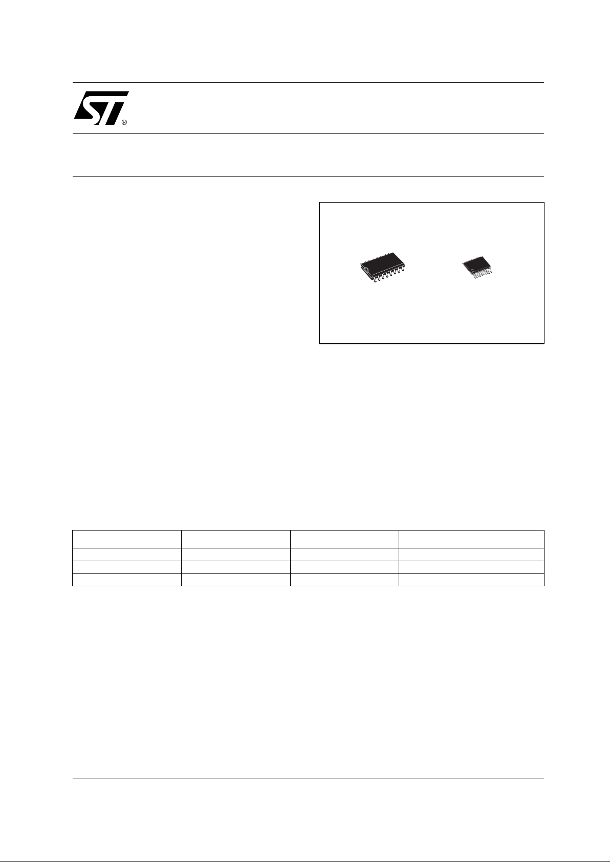
■ AVAILABLE IN SO-16L AND TSSOP20
■ SCSI BUS HOT PLUG-COMPATIBLE
DESCRIPTION
The SCSI-2 and SCSI-3 standards recommend
the use of active terminations at both ends of
every cable segment in a SCSI system with a
single-ended drivers and reveivers. The
ST21S07A SCSI terminator, which is fully
compliant with these standands, enables the
designer to gain the benefits of active termination:
greater immunity to voltages drop on the
TERMPWR (TERMination PoWeR) line,
enhanced high level noise immunity, intrinsic
TERMPWR decouplig, and very low quiescent
current consumption.
The ST21S07A integrates a regulator and nine
precise switched 110Ω termination resistors into a
monolithic IC. The ST21S07A can be electri cally
isolatesd from the SCSI bus without physical
removal from the SCSI device.
ORDERING CODES
(*) Avai l abl e on reque st
Type Temperature Range Package Comments
ST21S07ACW 0 to 70 °C SO-16L (Tube) 49parts per tube / 25tube per box
ST21S07ACWR 0 to 70 °C SO-16L (Tape & Reel) 1000 parts per reel
S21S07ACTR (*) 0 to 70 °C TSSOP20 (Tape & Reel) 2500 parts per reel
ST21S07A
SCSI TERMINATOR
SOP TSSOP
Page 2
ST21S07A
2/10
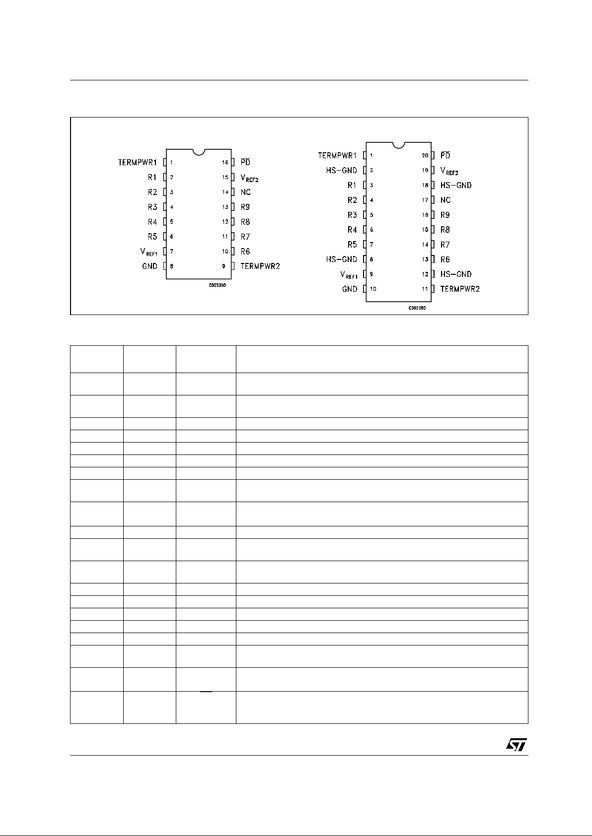
PIN CONFIGURATION
PIN DESCRIPTION
PlN N°
(TSSP20)
PlN N°
(SO-16L)
SYMBOL NAME AND FUNCTION
1 1 TERMPWR1 Termina tion Power 1: Should be connected to the SCSI TERMPWR line.
Must be decoupled with either a 2.2µF or 4.7µF. See Fig. 2.
2 HS-GND Heat Sink Ground: Internally connected to the mounting pad. Should be
either grounded or electrically isolated from the other circuitry.
32R1Signal Termination 1: 110 Ω Termination
43R2Signal Termination 2: 110 Ω Termination
54R3Signal Termination 3: 110 Ω Termination
65R4Signal Termination 4: 110 Ω Termination
76R5Signal Termination 5: 110 Ω Termination
8 HS-GND Heat Sink Ground: Internally connected to the mounting pad. Should be
either grounded or electrically isolated from the other circuitry.
97V
REF1
Reference Voltage 1: Must be external connected directly to the V
REF2
pin. Must be decoupoled with 4.7µF capacitor as shown in Figure 2
10 8 GND Ground: Signal groud: 0V
11 9 TERMPWR Termination Power21: Should be connected to the SCSI TERMPWR line.
Must be decoupled with either a 2.2µF or 4.7µF. See Fig. 2.
12 HS-GND Heat Sink Ground: Internally connected to the mounting pad. Should be
either grounded or electrically isolated from the other circuitry.
13 10 R6 Signal Termination 6: 110 Ω Termination
14 11 R7 Signal Termination 7: 110 Ω Termination
15 12 R8 Signal Termination 8: 110 Ω Termination
16 13 R9 Signal Termination 9: 110 Ω Termination
17 14 NC Not connected: Do not connect any signal to this pin
18 HS-GND Heat Sink Ground: Internally connected to the mounting pad. Should be
either grounded or electrically isolated from the other circuitry.
19 15 V
REF2
Reference Voltage 2: Must be external connected directly to the V
REF1
pin. Must be decoupoled with 4.7µF capacitor
20 16 PD
Power Down: When tied low, the ST21S07A enters a power down mode.
Contains an internal 60K pull-up. Strap low to deactivate the ST21S07A,
leave open circuited to activate the ST21S07A
SO-16L TSSOP20
Page 3
ST21S07A
3/10
ABSOLUTE MAXIMUM RATINGS
Absolute Maximum Ratings are those values beyond which damage to the device may occur. Functional operation under these condition is
not implied.
RECOMMENDED OPERATING CONDITIONS
DC CHARACTERISTICS (T
A
= 0 to 70°C, unless otherwise specified.)
REGULATOR CHARACTERISTICS (T
A
= 0 to 70°C, unless otherwise specified.)
Note 1: TERMPWR = 4V to 5.5V
Note2: Si gnal Lines = 0V to T ER M PWR
Note3: Al l signal lines = 0V
Note 4: Al l s i gnal lines open
Note 5: PD
= 0V
Note 6: Gua ranteed by design; not production t ested
Note 7: R
1
through R9 only
Note 8: R
1
through R9 and PD
Note 9: V
SIGNAL
= 0.2V
Symbol Parameter Value Unit
V
PIN
Voltage on Any Pin Relative to Ground
-1 to 7 V
T
stg
Storage Temperature Range
-55 to +150 °C
T
op
Operating Junction Temperature Range
0 to +70 °C
Symbol Parameter Test Conditions Min. Typ. Max. Unit
V
TP
TERMPWR Voltage 4 5.5 V
V
PDA
PD Active -0.3 0.8 V
V
PDI
PD Inactive 2 VTP+0.3 V
Symbol Parameter Test Conditions Min. Typ. Max. Unit
I
TP
TERMPWR Current (note 1, 3)
(note 1, 4) 1.5
250
8
mA
mA
I
PD
Power Down Current (note 1, 2, 5) 70 150 µA
R
TERM
Termination Resistance (note 1, 2) 108 110 112 Ω
T
SD
Die Thermal Shutdown (note 1, 6) 150 170 °C
C
PD
Power Down Termniatio N
Capacitance
(note 1, 2, 5, 6) 3 5 pF
H
PD
Power Down Hysteresis (note 1) 280 mV
I
IH
Input Leackage High (note 1, 8) -1 µA
I
IL
Input Leackage Low (note 1, 7) 1 µA
Symbol Parameter Test Conditions Min. Typ. Max. Unit
V
REF
Output Voltage (note 1, 2) 2.79 2.85 2.93 V
v
DROP
Drop-out Voltage (note 3, 6) 0.3 0.75 V
LI
REG
Line Regulation (note 1, 4) 0.25 2 %
LO
REG
Load Regulatio (note 1, 2) 0.5 3 %
I
LIM
Current Limit (note 1) 450 mA
I
SINK
Sink Current (note 1) 200 mA
I
OUT
Output Current (note9) 25.2 mA
Page 4

ST21S07A
4/10
FUNCTIONAL DESCRIPTION
The ST21S07A consists of a bandgap reference,
buffer amplifier, and nine termination resistors
Figure 1). The bandgap reference circuit produces
a precise 1.25V level which is fed to a buffer
amplifier. The bu ffer prod uc e a 2.85V level and is
capable of sourcing at least 24mA into each of the
termination resistors when the signal line is low
(active). When the driver for a given signal line
turns off, the terminator will pull the signal line to
2.85V (quiescent state). To handle actively
negated SCSI signals, the buffer can sink 200mA.
When all lines settle in the quiescent state, the
regulator will consume about 1.5mA. When the
ST21S07A is put into power-down mode by
bringing PD
low, the power-down circuitry will turn
off the transistors on each signal line. This will
isolated the ST21S 07A from the signal l ines and
effectively remove it from the circuit. The
power-down pin (PD
) has an internal pull-up
resistor.To place the ST21S07A into an active
state, the PD
pin should be left open circuited.
To ensure proper operation, both the TERMPWR1
and TERMPWR2 pins must be connecte d to the
SCSI bus TREMPWR line and both the VREF1
and VREF2 pins must be tied together externally.
Each ST21S07A requires a 4.7µF capacitor
connected between the VREF pins and ground.
Figure 2 details a typical SCS I bus configuration.
In an 8-bit wide SCSI bus arrangement ("A"
Cable), two ST21S07A’s would be needed at each
end of the SCSI cable in order to terminate the 18
active signal lines. In a 16-bit SCSI bus
arrangement ("P" Cable), three ST21S07A’s
would be need at e ach end of the SCSI cable in
order to terminate the 27 active signal lines.
Figure 1 : Block Diagram
Page 5

ST21S07A
5/10
Figure 2 : Typical Scsi Bus Configuraion
NOTES:
1) C
1
= 4.7µF tantalium C2 = 2.2µF tantali um or 4.7mF alumi num
2) If the ST21S07A is to be embedded into a peripheral that will act as a target on a SCSI bus, it is that recommended TERMPWR be derive d
from the SCSI cable, not generated locally. In this configuration, if a power failure occurs in the peripheral, it will not affect the bus.
3) A high frequency by pass capaci tor (0.1µF recommended) can be added in parallel to C1 for applications using fast rise/f al l tim e drivers.
Page 6

ST21S07A
6/10
DIM.
mm inch
MIN. TYP. MAX. MIN. TYP. MAX.
A2.650.104
a1 0.1 0.2 0.004 0.008
a2 2.45 0.096
b 0.35 0.49 0.014 0.019
b1 0.23 0.32 0.009 0.012
C0.5 0.020
c1 45 (typ.)
D 10.1 10.5 0.397 0.413
E 10.0 10.65 0.3.93 0.419
e1.27 0.050
e3 8.89 0.350
F 7.4 7.6 0.291 0.300
L 0.5 1.27 0.020 0.050
M0.750.029
S8 (max.)
P013I
SO16L MECHANICAL DATA
Page 7

ST21S07A
7/10
DIM.
mm inch
MIN. TYP. MAX. MIN. TYP. MAX.
A1.10.433
A1 0.05 0.10 0.15 0.002 0.004 0.006
A2 0.85 0.9 0.95 0.335 0.354 0.374
b 0.19 0.30 0.0075 0.0118
c 0.09 0.2 0.0035 0.0079
D 6.4 6.5 6.6 0.252 0.256 0.260
E 6.25 6.4 6.5 0.246 0.252 0.256
E1 4.3 4.4 4.48 0.169 0.173 0.176
e 0.65 BSC 0.0256 BSC
K0
o
4
o
8
o
0
o
4
o
8
o
L 0.50 0.60 0.70 0.020 0.024 0.028
c
E
b
A2
A
E1
D
1
PIN 1 IDENTIFICATION
A1
L
K
e
TSSOP20 MECHANICAL DATA
Page 8

ST21S07A
8/10
Page 9

ST21S07A
9/10
Page 10

ST21S07A
10/10
Information furnished is bel ieved to be accurate and reliable. However, STMicroe lectronics assumes no responsibility for the
consequences of use of such information nor for any infringement of patents or other rights of third parties which may result from
its use. No li cense is granted by i mp lication or otherwise under any patent or patent rights of STMicroelectronics. Specifications
mentioned in this publication ar e subject to change without notice. This publication supersedes and replaces all information
previously supplied. S TMicroelectronics products are not authorized for use as critica l components in life suppo rt devices or
systems without express written approval of STMicroelectronics.
© The ST logo is a registered trademark of STMicroelectronics
© 2001 STM icroelectronics - P rinted in Italy - All Righ ts Reserv ed
STMicr o el ectronics GROUP OF COMPA NI E S
Australi a - Brazil - Chi na - Finlan d - F rance - Germ any - Hong Kong - India - Ital y - Japan - Ma l aysia - Malta - Morocco
Singapo re - Spain - Sweden - Swit zerland - United Kingdom
© http://www.st.com
 Loading...