

Datasheet ST2100C42R3, ST2100C42R2L, ST2100C42R2, ST2100C42R1, ST2100C42R0L Datasheet (International Rectifier)
...Page 1
Bulletin I25198/A
Next Data SheetIndex
Previous Datasheet
To Order
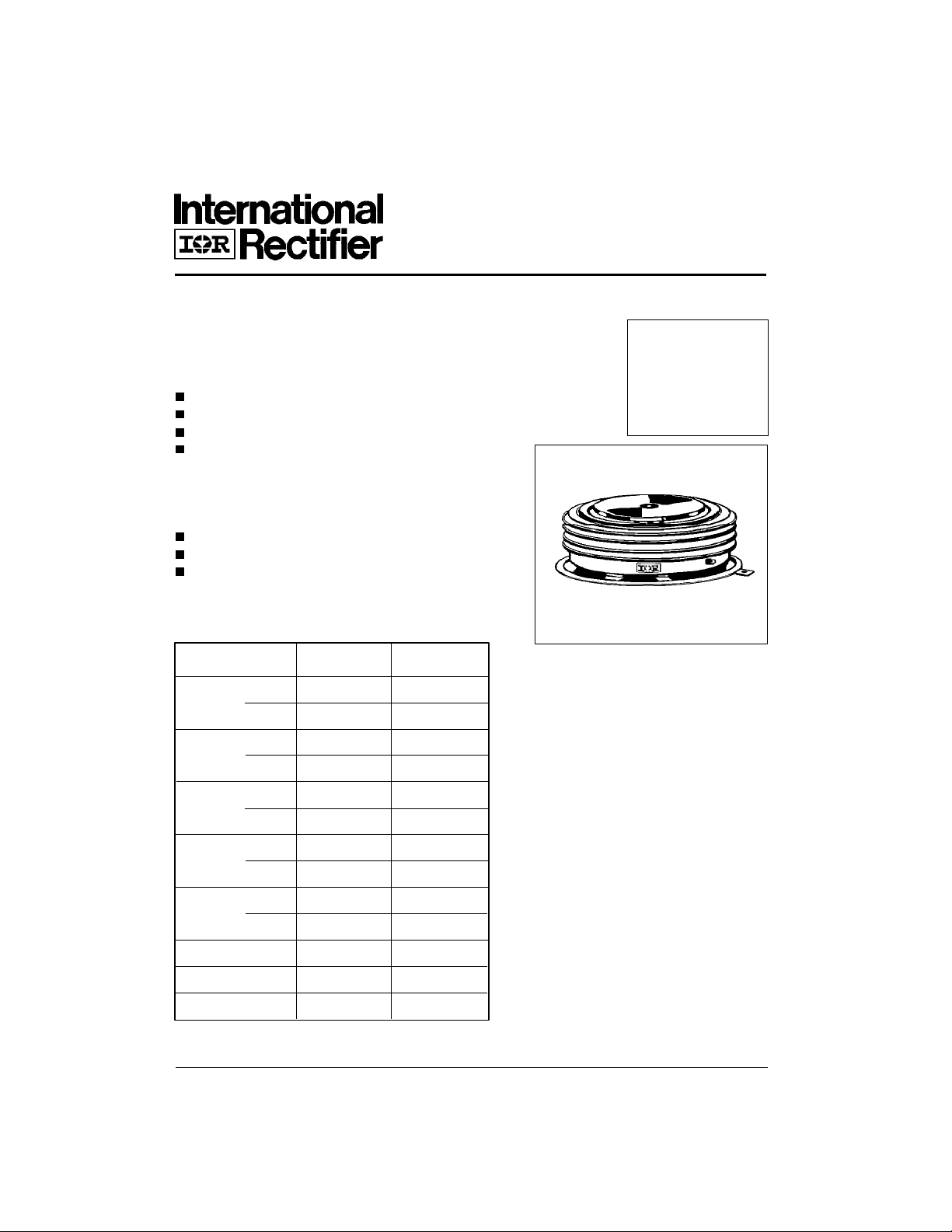
ST2100C..R SERIES
PHASE CONTROL THYRISTORS Hockey Puk Version
Features
Double side cooling
High surge capability
High mean current
Fatigue free
Typical Applications
DC motor controls
Controlled DC power supplies
AC controllers
Major Ratings and Characteristics
Parameters ST2100C..R Units
I
T(AV)
@ T
C
I
T(AV)
@ T
hs
I
T(RMS)
@ T
hs
I
TSM
2
I
t @ 50Hz 6570 KA2s
@ 50Hz 36250 A
@
60Hz 38000 A
1770 A
80 °C
2090 A
55 °C
3850 A
25 °C
2090A
(R-PUK)
V
DRM/VRRM
t
q
T
J
@
60Hz 5990 KA2s
3000 to 4200 V
typical 500 µs
max. 125 °C
D-413
Page 2

ST2100C..R Series
Next Data SheetIndex
Previous Datasheet
To Order
ELECTRICAL SPECIFICATIONS
Voltage Ratings
Voltage V
DRM/VRRM
Type number Code peak and off-state voltage repetitive peak voltage
30 3000 3100
32 3200 3300
34 3400 3500
ST2100C..R 250
36 3600 3700
38 3800 3900
40 4000 4100
42 4200 4300
, max. repetitive V
, maximum non- I
RSM
DRM/IRRM
@ TC = 125°C
V V mA
max.
On-state Conduction
Parameter ST2100C..R Units Conditions
I
Max. average on-state current 1770 (1150) A
T(AV)
@ Case temperature 80 °C
I
Max. average on-state current 2090 (940) A
T(AV)
@ Heatsink temperature 55 (85) °C
I
Max. RMS on-state current 3850 A DC @ 25°C heatsink temperature double side cooled
T(RMS)
I
Max. peak, one-cycle No voltage
TSM
non-repetitive surge current reapplied
2
t Maximum I2t for fusing No voltage Initial TC = 125°C
I
Max. value of threshold voltage 1.03 V TJ = TJ max.
V
T(TO)
r
Max. value of on-state slope
t
resistance
V
Max. on-state voltage 1.875 V Ipk= 2900A, TC = 25°C
TM
I
Typical latching current 300 mA TJ = 25°C, VD = 5V
L
36250
38000
29000
30350
6570
5990
4205
3820
0.32 TJ = TJ max.
180° conduction, half sine wave
double side (single side [anode side]) cooled
t = 10ms
t = 8.3ms
A
KA2s
mΩ
t = 10ms
t = 8.3ms
t = 10ms
t = 8.3ms
t = 10ms
t = 8.3ms
50% V
RRM
reapplied Sinusoidal half wave,
reapplied
50% V
RRM
reapplied
Switching
Parameter ST2100C..R Units Conditions
di/dt Max. repetitive 50Hz (no repetitive) From 67% V
rate of rise of turned-on current T
t
Maximum delay time 2.5
d
t
Typical turn-off time 500
q
150 (300) A/µs
µs
= TJ max.
J
Gate drive 30V, 15Ω,
Rise time 0.5µs
I
= 1000A, tp = 1ms, TJ = TJ max, V
T
dI
/dt = 2A/µs, V
RR
to 1000A gate drive 20V, 10Ω, tr = 0.5µs
DRM
DR =
Vd = 67% V
67% V
DRM, dVDR
DRM, TJ
/dt = 8V/µs linear
2222222222222
= 25°C
= 50V,
RM
12
D-414
Page 3

ST2100C..R Series
To Order
Next Data SheetIndex
Previous Datasheet
Fig. 1 - Current Ratings Characteristics Fig. 2 - Current Ratings Characteristics
Fig. 3 - On-state Power Loss Characteristics
Fig. 5 - Maximum Non-Repetitive Surge Current Fig. 6 - Maximum Non-Repetitive Surge Current
D-417
Fig. 4 - On-state Voltage Drop Characteristics
Page 4

ST2100C..R Series
To Order
Next Data SheetIndex
Previous Datasheet
Fig. 7 - Stored Charged
Fig. 8 - Thermal Impedance Z
Fig. 9 - Gate Characteristics
D-418
Characteristics
thJ-C
Page 5

Blocking
To Order
Next Data SheetIndex
Previous Datasheet
Parameter ST2100C..R Units Conditions
dv/dt Maximum linear rate of rise of
off-state voltage
I
Max. peak reverse and off-state
RRM
I
leakage current
DRM
500 V/µs TJ = TJ max. to 67% rated V
250 mA TJ = 125°C rated V
Triggering
Parameter ST2100C..R Units Conditions
P
Maximum peak gate power 150 tp = 100µs
GM
P
Maximum average gate power 10
G(AV)
I
Max. peak positive gate current 30 A Anode positive with respect to cathode
GM
V
Max. peak positive gate voltage 30 V Anode positive with respect to cathode
GM
-V
Max. peak negative gate voltage 0.25 V Anode positive with respect to cathode
GM
I
Maximum DC gate current
GT
required to trigger
V
Maximum gate voltage required
GT
to trigger
V
DC gate voltage not to trigger 0.25 V TC = 125°C
GD
400 mA TC = 25°C, V
4 V T
W
= 25°C, V
C
ST2100C..R Series
DRM
applied
DRM/VRRM
= 5V
DRM
= 5V
DRM
Max. gate current/voltage not to
trigger is the max. value which
will not trigger any unit with rated
V
anode-to-cathode applied
DRM
23
Thermal and Mechanical Specification
Parameter ST2100C..R Units Conditions
TJ max. Max. operating temperature 125 On-state (conducting)
T
Max. storage temperature range -55 to 125
stg
R
Thermal resistance, junction 0.019 DC operation single side cooled
thJ-C
to case 0.0095 DC operation double side cooled
R
Thermal resistance, case 0.004 Single side cooled
th(C-h)
to heatsink 0.002 Double side cooled
F Mounting force ± 10%
wt Approximate weight 1600 g
Case style (R-PUK) See Outline Table
∆R
Conduction
thJ-C
(The following table shows the increment of thermal resistence R
43000
(4400)
°C
K/W
K/W
N
(Kg)
when devices operate at different conduction angles than DC)
thJ-C
Conduction angle Single side Double side Units Conditions
180° 0.0010 0.0010 T
120° 0.0017 0.0017 K/W
60° 0.0044 0.0044
J
D-4153333
Clamping force 43KN with
mounting compound
= TJ max.
Page 6

ST2100C..R Series
37.7 (1.5) M A X.
6
.
3
(
0
.
2
4
)
To Order
Next Data SheetIndex
Previous Datasheet
Ordering Information Table
Device Code
ST 210 0 C 42 R 1
1 - Thyristor
2 - Essential part number
3 - 0 = Converter grade
4 - C = Ceramic Puk
5 - Voltage code: Code x 100 = V
6 - R = Puk Case
7 - 0 = Eyelet terminals (Gate and Auxiliary Cathode Unsoldered Leads)
8 - Critical dv/dt: None = 500V/µsec (Standard selection)
Outline Table
2 3
(See Voltage Rating Table)
RRM
1 = Fast-on terminals (Gate and Auxiliary Cathode Unsoldered Leads)
2 = Eyelet terminals (Gate and Auxiliary Cathode Soldered Leads)
3 = Fast-on terminals (Gate and Auxiliary Cathode Soldered Leads)
L = 1000V/µsec (Special selection)
112.5 (4.4) DIA. MAX.
73.2 (2.9) DIA. MAX.
TWO PLACES
51
4
768
GATE
1.5 (0.06) DIA.
12
CATHODE
3.7 (0.15) DIA. NOM. X
2.1 (0.1) DEEP MIN.
BOTH ENDS
ANODE
HOLE 1.5 (0.06)
DIA. MAX.
4.76 (0.2)
2222222222222
20° ± 5°
(R-PUK)
All dimensions in millimeters (inches)
D-416
 Loading...