

Page 1
ST202E
■ ESDPROTECTIONFORRS-232I/OPINS:
±
15KV HUMANBODYMODEL
■ GUARANTEED120kbpsDATERATE
■ GUARANTEEDSLEWRATERANGE3 to
30V/µs
■ OPERATEFROMA SINGLE5VPOWER
SUPPLY
DESCRIPTION
The ST202E/ST232E are a 2 driver 2 receiver
devices designed for RS-232 and V.28
communications in harsh enviroments. Each
transmitter output and receiver input is protected
against ± 15KV electrostatic discharge (ESD)
shocks. The drivers meet all EIA/TIA-232E and
CCITT V.28 specifications at data rates up to
120Kbps, when loaded in accordance with the
EIA/TIA-232Especification.
The ST202E/232E use a single 5V supply
voltage.
The ST232E operates with four 1µF capacitors,
ST232E
± 15KVESD PROTECTED
5V RS-232 TRANSCEIVER
N
(PlasticPackage)
(Micro Package)
W
(Micro Package Large)T(TSSOPPackage)
while the ST202E operates with four 0.1µF
capacitors, further reducing cost and board
space.
D
ORDERCODES
Typ e Temp erature
Range
ST202ECN ST232ECN 0 to 70
ST202EBN ST232EBN -40 to 85
ST202ECD ST232ECD 0 to 70
ST202EBD ST232EBD -40 to 85
ST202ECDR ST232ECDR 0 to 70
ST202EBDR ST232EBDR -40 to 85
ST202ECW ST232ECW 0 to 70
ST202EBW ST232EBW -40 to 85
ST202ECWR ST232ECWR 0 to 70
ST202EBWR ST232EBWR -40 to 85
ST202ECTR ST232ECTR 0 to 70
ST202EBTR ST232EBTR -40 to 85
April 2000
Package Comments
o
C DIP-16 25 parts per tube / 40 tube per box
o
C DIP-16 25 parts per tube / 40 tube per box
o
C SO-16 (Tube) 50 parts per tube / 20 tube per box
o
C SO-16 (Tube) 50 parts per tube / 20 tube per box
o
C SO-16 (Tape & Reel) 2500 parts per reel
o
C SO-16 (Tape & Reel) 2500 parts per reel
o
C SO-16 Large (Tube) 50 parts per tube / 20 tube per box
o
C SO-16 Large (Tube) 50 parts per tube / 20 tube per box
o
C SO-16 Large (Tape & Reel) 1000 parts per reel
o
C SO-16 Large (Tape & Reel) 1000 parts per reel
o
C TSSOP16 (Tape & Reel) 2500 parts per reel
o
C TSSOP16 (Tape & Reel) 2500 parts per reel
1/12
Page 2
ST202E/ST232E
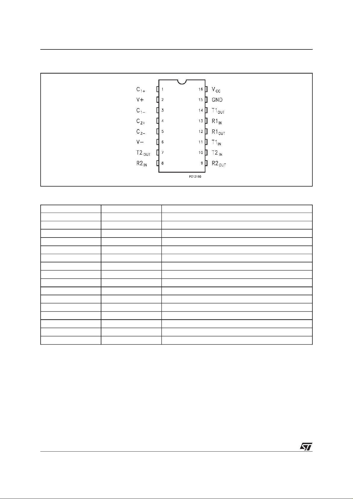
PIN CONFIGURATION
PIN DESCRIPTION
PIN No SYMBOL NAM E AND FUNC T I O N
1C
2 V+ Doubled Voltage Terminal
3C
4C
5C
6 V- Inverted Voltage Terminal
7T2
8R2
9R2
10 T2
11 T1
12 R1
13 R1
14 T1
15 GND Ground
16 V
+ Positive Terminal for the first Charge Pump Capacitor
1
- Negative Terminal for the first Charge Pump Capacitor
1
+ Positive Terminal for the second Charge Pump Capacitor
2
- Negative Terminal for the second Charge Pump Capacitor
2
OUT
IN
OUT
IN
IN
OUT
IN
OUT
CC
Second Transmitter Output Voltage
Second Receiver Input Voltage
Second Receiver Output Voltage
Second Transmitter Input Voltage
First Transmitter Input Voltage
First Receiver Output Voltage
First Receiver Input Voltage
First Transmitter Output Voltage
Supply Voltage
2/12
Page 3
ST202E/ST232E
ABSOLUTE MAXIMUM RATINGS
(Note 1)
Symb o l Para met er Val u e Uni t
V
V
V
T
R
T
OUT
R
OUT
T
SCTOUT
T
AbsoluteMaximumRatingsarethosevaluesbeyond whichdamagetothedevicemay occur. Functionaloperationunderthese condition isnot implied.
Supply Voltage -0.3 to 6 V
CC
Extra Positive Voltage (VCC-0.3) to 14 V
+
Extra Negative Voltage -14 to 0.3 V
-
Transmitter Input Voltage Range -0.3 to (V+ + 0.3) V
IN
Receiver Input Voltage Range ±30 V
IN
Transmitter Output Voltage Range (V- - 0.3) to (V+ + 0.3) V
Receiver Output Voltage Range -0.3 to (VCC+ 0.3) V
Short Circuit Duration on T
Storage Temperature Range -65 to +150
stg
OUT
infinite
o
C
ELECTRICAL CHARACTERISTICS
(C
unlessotherwise specified.TypicalValus are referredto T
Symbol Parameter Test Conditio ns Value Unit
= 0.1µF for ST202E,C1-C4=1µF forST232E, VCC=5V±10% TA= -40 to 85oC,
1-C4
=25oC)
A
Min. Typ. M ax.
I
SUPPLYVCC
Power Supply Current No Load, TA=25oC 5 10 mA
TRANSMITTER ELECTRICAL CHARACTERISTICS
(C
unlessotherwise specified.TypicalValus are referredto T
Symbol Parameter Test Conditio ns Value Unit
Note1:Measured from3Vto-3Vorfrom-3V to3V.
Note2: One trasmitter output isloaded with R
= 0.1µF for ST202E,C1-C4=1µF forST232, VCC=5V±10%, TA= -40 to 85oC,
1-C4
=25oC)
A
Min. Typ. M ax.
V
Output Voltage Swing All Transmitter outputs are loaded
TOUT
±5 ±9V
with 3KΩto GND
Logic Pull-Up Current TIN=0VtoV
I
V
V
SR
D
TIL
Input Logic Threshold Low 0.8 V
TIL
Input Logic Threshold High 2 V
TIH
Transition Slew Rate TA=25oC, VCC=5V,
T
Data Rate RL=3to7KΩ,CL= 50 to 1000 pF
R
=3to7KΩ,
R
L
= 50 to 1000 pF (Note 1)
C
L
CC
230 400 Kbits/s
one trasmitter switching
R
Transmitter Output Resistance VCC= V+ = V- = 0V
TOUT
Transmitter Output Short
I
SC
V
OUT
=±2V
300
Circuit Current
Trasmitter Propagation Delay RL=3KΩ,CL= 2500 pF
t
DT
All trasmitter loaded
=3KΩ to7KΩ,CL= 50 to 1000pF
L
10
±
A
µ
3 6 30 V/µs
Ω
10
±
2
60 mA
±
A
µ
3/12
Page 4

ST202E/ST232E
RECEIVERELECTRICAL CHARACTERISTICS
(C
unlessotherwise specified. TypicalValus are referred to T
Symbol Parameter Test Conditio ns Value Unit
= 0.1µF for ST202E,C1-C4=1µF forST232E, VCC=5V±10%, TA= -40 to 85oC,
1-C4
=25oC)
A
Min. Typ. M ax.
V
Receiver Input Voltage
RIN
-30 30 V
Operating Range
R
V
RS-232 Input Resistance TA=25oC, VCC=5V 357K
RIN
RS-232 Input Logic Threshold
RIL
TA=25oC, VCC= 5 V 0.8 1.2 V
Low
V
RS-232 Input Logic Threshold
RIH
TA=25oC, VCC= 5 V 1.7 2.4 V
High
V
V
RS-232 Input Hysteresis VCC= 5 V 0.2 0.5 1 V
RIHYS
TTL/CMOS Output Voltage
ROL
I
= 3.2mA 0.4 V
OUT
Low
V
TTL/CMOS Output Voltage
ROH
I
= -1mA 3.5 VCC-0.4 V
OUT
High
Propagation Delay Time CL=150pF 0.5 10 µs
t
dR
Ω
4/12
Page 5

ST202E/ST232E
APPLICATION CIRCUITS
TTL / CMOS INPUTS
(note 1, note2)
C5
1
C1+
+
C1
3
C1-
4
C2+
+
C2
C2-
5
11
IN
T1
IN
T2
10
+5V INPUT
+
Vcc
+5V TO +10V
VOLTAGE
DOUBLER
+10V TO -10V
VOLTAGE
INVERTER
T1
T2
16
C3
T1
T2OUT
+
V+
V-
OUT
2
6
C4
14
7
+10V
-10V
+
RS 232 OUTPUTS
IN
R1
TTL / CMOSOUTPUTS
12
9
R1
R2
OUT
OUT
R1
R2
5K
R2
13
RS 232 INPUTS
IN
8
5K
GND
15
Note1:C
Note2:C
capacitorscanevenbe1 µFones.
1-4
canbecommonorbiasedcapacitors.
1-4
CapacitanceValue (µF)
DEVICESC1C2C3C4C5
ST202E 0.1 0.1 0.1 0.1 0.1
ST232E 1 1 1 1 1
5/12
Page 6

ST202E/ST232E
SupplyCurrent vs Temperature
ReceiverPropagationDelay
DataRate vs Temperature
DriverPropagationDelay
HighLevel Output Voltage Swing vs Temperature
6/12
Low Level Output Voltage Swing vs Temperature
Page 7

ST202E/ST232E
HighLevel Trasmitter Output Short Circuit
Currentvs Temperature
HighLevel Receiver Output Short Circuit Current
vs Temperature
Low Level Trasmitter OutputShort Circuit
Currentvs Temperature
Low Level Receiver OutputShort Circuit Current
vs Temperature
7/12
Page 8

ST202E/ST232E
Plastic DIP-16 (0.25) MECHANICAL DATA
DIM.
MIN. TYP. MAX. MIN. TYP. MAX.
a1 0.51 0.020
B 0.77 1.65 0.030 0.065
b 0.5 0.020
b1 0.25 0.010
D 20 0.787
E 8.5 0.335
e 2.54 0.100
e3 17.78 0.700
F 7.1 0.280
I 5.1 0.201
L 3.3 0.130
Z 1.27 0.050
mm inch
8/12
P001C
Page 9

SO-16 MECHANICAL DATA
ST202E/ST232E
DIM.
MIN. TYP. MAX. MIN. TYP. MAX.
A 1.75 0.068
a1 0.1 0.2 0.004 0.007
a2 1.65 0.064
b 0.35 0.46 0.013 0.018
b1 0.19 0.25 0.007 0.010
C 0.5 0.019
c1 45 (typ.)
D 9.8 10 0.385 0.393
E 5.8 6.2 0.228 0.244
e 1.27 0.050
e3 8.89 0.350
F 3.8 4.0 0.149 0.157
G 4.6 5.3 0.181 0.208
L 0.5 1.27 0.019 0.050
M 0.62 0.024
S 8 (max.)
mm inch
P013H
9/12
Page 10

ST202E/ST232E
SO16L MECHANICAL DATA
DIM.
MIN. TYP. MAX. MIN. TYP. MAX.
A 2.65 0.104
a1 0.1 0.2 0.004 0.008
a2 2.45 0.096
b 0.35 0.49 0.014 0.019
b1 0.23 0.32 0.009 0.012
C 0.5 0.020
c1 45 (typ.)
D 10.1 10.5 0.397 0.413
E 10.0 10.65 0.3.93 0.419
e 1.27 0.050
e3 8.89 0.350
F 7.4 7.6 0.291 0.300
L 0.5 1.27 0.020 0.050
M 0.75 0.029
S 8 (max.)
mm inch
10/12
P013I
Page 11

TSSOP16 MECHANICAL DATA
ST202E/ST232E
DIM.
mm inch
MIN. TYP. MAX. MIN. TYP. MAX.
A 1.1 0.433
A1 0.05 0.10 0.15 0.002 0.004 0.006
A2 0.85 0.9 0.95 0.335 0.354 0.374
b 0.19 0.30 0.0075 0.0118
c 0.09 0.20 0.0035 0.0079
D 4.9 5 5.1 0.193 0.197 0.201
E 6.25 6.4 6.5 0.246 0.252 0.256
E1 4.3 4.4 4.48 0.169 0.173 0.176
e 0.65 BSC 0.0256 BSC
K0
o
o
4
o
8
o
0
o
4
8
L 0.50 0.60 0.70 0.020 0.024 0.028
o
A2
A
A1
PIN 1 IDENTIFICATION
b
e
c
K
L
E
D
E1
1
11/12
Page 12

ST202E/ST232E
Information furnished isbelieved to be accurate and reliable. However,STMicroelectronics assumes no responsibility forthe consequences
of use of such information nor for any infringement of patents or other rights of third parties which may result from its use. No license is
granted by implication or otherwise under any patent or patent rights of STMicroelectronics. Specification mentioned in thispublication are
subject tochange without notice. Thispublication supersedes and replaces all information previously supplied.STMicroelectronics products
are not authorized for use as criticalcomponents in lifesupport devices or systems withoutexpress written approval of STMicroelectronics.
The ST logo isa registered trademark of STMicroelectronics
2000 STMicroelectronics – Printed in Italy – All Rights Reserved
STMicroelectronics GROUP OF COMPANIES
Australia - Brazil- China - Finland - France - Germany - Hong Kong - India - Italy - Japan- Malaysia - Malta - Morocco
Singapore - Spain- Sweden - Switzerland - United Kingdom - U.S.A.
http://www.st.com
.
12/12
 Loading...