

Page 1
HIGH VOLTAGE FAST-SWITCHING
■ NEWSERIES, ENHANCHED
PERFORMANCE
■ FULLYINSULATEDPACKAGEFOREASY
MOUNTING
■ HIGH VOLTAGECAPABILITY
■ HIGH SWITCHING SPEED
■ TIGTHERhfe CONTROL
■ IMPROVEDRUGGEDNESS
APPLICATIONS:
■ HORIZONTAL DEFLECTIONFOR COLOR
TV
DESCRIPTION
The device is manufactured using Diffused
Collector Technology for more stable operation
Vs base drive circuit variations resulting in very
low worstcase dissipation.
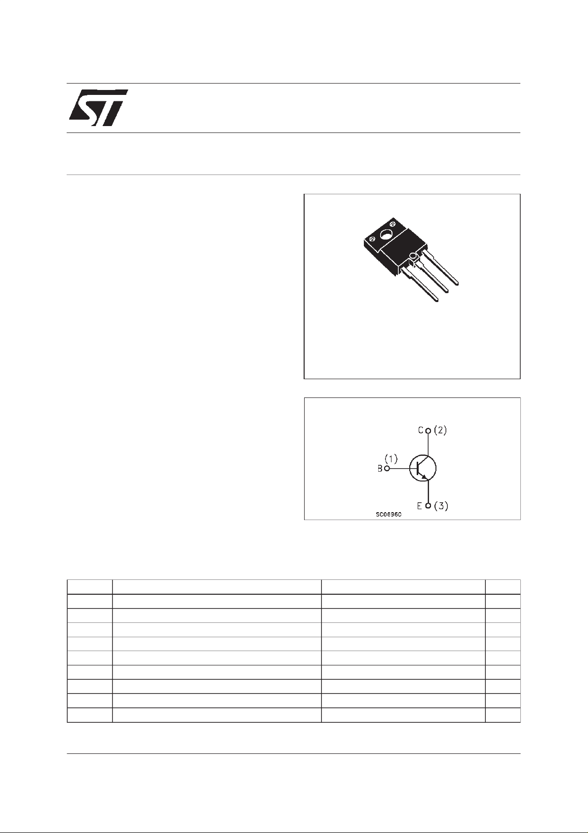
ST1802HI
NPN POWER TRANSISTOR
3
2
1
ISOWATT218
INTERNAL SCHEMATIC DIAGRAM
ABSOLUTE MAXIMUM RATINGS
Symbol Parameter Value Unit
V
V
V
I
P
T
January 2000
Collect or-Base Voltage (IE= 0) 1500 V
CBO
Collect or-Emit ter V oltage (IB= 0) 600 V
CEO
Emitter-Base Vol tage (IC=0) 7 V
EBO
I
Collect or Current 10 A
C
Collect or Peak Cu rr ent (tp<5ms) 15 A
CM
Base Current 4 A
I
B
Tot al Dissipation at Tc=25oC50W
tot
Storage Temperature -65 to 150
stg
T
Max. Ope r ating Junct ion T emperature 150
j
o
C
o
C
1/6
Page 2
ST1802HI
THERMAL DATA
R
thj-case
Ther mal Resist ance Junction-c a se Max 2.5
o
C/W
ELECTRICAL CHARACTERISTICS (T
=25oC unlessotherwise specified)
case
Symbol Parameter Test Cond itions Min. Typ. Max. Un it
I
CES
I
EBO
V
CEO(sus)
Collec t or Cut -off
Current (V
BE
=0)
Emitt er Cut -of f Cu rrent
=0)
(I
C
∗ Collector- Emitt er
V
= 1500 V
CE
= 1500 V Tj=125oC
V
CE
V
=7V 1 mA
EB
I
= 100 m A L = 25 mH 600 V
C
1
2
Sust aining V o lt age
=0)
(I
B
∗ Co llector-E mitter
V
CE(sat)
Saturation Voltage
V
∗ Base-Emi tter
BE(sat)
IC=4A IB=0.8A
=4A IB=1.2A
I
C
IC=4.5A IB=1A 1.2 V
5
1.5
Saturation Voltage
∗ DC C ur rent Gain IC=1A VCE=5V
h
FE
INDUCTIV E LO AD
t
∗
Pulsed: Pulse duration = 300 µs, duty cycle1.5 %
s
t
f
Storage Ti me
Fall Time
=5A VCE=5V 4
I
C
IC=4A I
=5 µHVBB=-2.5V
L
B
f=16KHz
Bon(END)
=1A
25
5
0.3
9
6
0.5
mA
mA
V
µs
µs
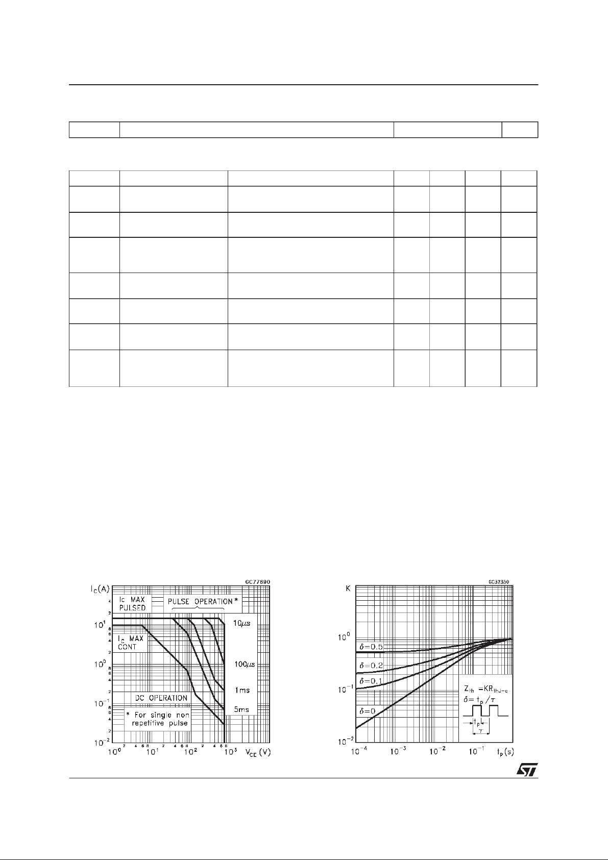
Safe Operating Area ThermalImpedance
2/6
Page 3

ST1802HI
Derating Curve
CollectorEmitter Saturation Voltage
BaseEmitter Saturation Voltage
DC Current Gain
PowerLosses At 16 KHz
SwitchingTime InductiveLoad
3/6
Page 4

ST1802HI
ReverseBiased SOA
InductiveLoad SwitchingTest Circuits.
4/6
Page 5

ISOWATT218 NARROW LEADS MECHANICAL DATA
ST1802HI
DIM.
A 5.35 5.65 0.211 0.222
C 3.30 3.80 0.130 0.150
D 2.90 3.10 0.114 0.122
D1 1.88 2.08 0.074 0.082
E 0.75 0.95 0.030 0.037
F 0.75 0.95 0.030 0.037
F2 1.50 1.70 0.059 0.067
F3 1.90 2.10 0.075 0.083
F5 1.10 0.043
G 10.80 11.20 0.425 0.441
H 15.80 16.20 0.622 0.638
L 9 0.354
L1 20.80 21.20 0.819 0.835
L2 19.10 19.90 0.752 0.783
L3 22.80 23.60 0.898 0.929
L4 40.50 42.50 1.594 1.673
L5 4.85 5.25 0.191 0.207
L6 20.25 20.75 0.797 0.817
N 2.1 2.3 0.083 0.091
R 4.6 0.181
DIA 3.5 3.7 0.138 0.146
MIN. TYP. MAX. MIN. TYP. MAX.
mm inch
- Weight: 4.9 g (typ.)
- MaximumTorque (applied to mounting flange) Recommended: 0.8 Nm; Maximum:1 Nm
- Theside of the dissipator must beflatwithin 80 µm
P025C/B
5/6
Page 6

ST1802HI
6/6
Information furnished is believed to be accurate and reliable. However, STMicroelectronics assumes no responsibility for theconsequences
of use of such information nor for any infringement of patents or other rights of third partieswhich may result from its use. No license is
granted by implication or otherwise under anypatent or patent rights of STMicroelectronics. Specification mentioned in this publication are
subject to change without notice. This publication supersedes and replaces allinformation previously supplied. STMicroelectronics products
are not authorized for use as critical components in life support devices orsystems without express written approval of STMicroelectronics.
Australia - Brazil - China - Finland - France - Germany- HongKong - India - Italy - Japan- Malaysia - Malta - Morocco-
The ST logo is a trademark of STMicroelectronics
2000 STMicroelectronics– Printed in Italy – All Rights Reserved
STMicroelectronicsGROUP OF COMPANIES
Singapore- Spain - Sweden - Switzerland - United Kingdom - U.S.A.
http://www.st.com
 Loading...