


A
8 Mbit Firmware Hub
Microchip Technology Company
The SST49LF008A flash memory devices are designed to be read-compatible
with the Intel® 82802 Firmware Hub (FWH) device for PC-BIOS application.
These devices provide protection for the storage and update of code and data in
addition to adding system design flexibility through five general purpose inputs.
Two interface modes are supported by the SST49LF008A: Firmware Hub (FWH)
Interface mode for in-system programming and Parallel Programming (PP) mode
for fast factory programming of PC-BIOS applications.
Features
• Firmware Hub for Intel 8xx Chipsets
• 8 Mbit SuperFlash memory array for code/data
storage
– 1024K x8
• Flexible Erase Capability
– Uniform 4 KByte Sectors
– Uniform 64 KByte overlay blocks
– 64 KByte Top Boot Block protection
– Chip-Erase for PP Mode Only
• Single 3.0-3.6V Read and Write Operations
• Superior Reliability
– Endurance:100,000 Cycles (typical)
– Greater than 100 years Data Retention
• Low Power Consumption
– Active Read Current: 6 mA (typical)
– Standby Current: 10 µA (typical)
• Fast Sector-Erase/Byte-Program Operation
– Sector-Erase Time: 18 ms (typical)
– Block-Erase Time: 18 ms (typical)
– Chip-Erase Time: 70 ms (typical)
– Byte-Program Time: 14 µs (typical)
– Chip Rewrite Time: 15 seconds (typical)
– Single-pulse Program or Erase
– Internal timing generation
SST49LF008A
Data Sheet
• Two Operational Modes
– Firmware Hub Interface (FWH) Mode for
In-System operation
– Parallel Programming (PP) Mode for fast
production programming
• Firmware Hub Hardware Interface Mode
– 5-signal communication interface supporting byte Read
and Write
– 33 MHz clock frequency operation
– WP# and TBL# pins provide hardware write
protect for entire chip and/or top Boot Block
– Block Locking Register for all blocks
– Standard SDP Command Set
– Data# Polling and Toggle Bit for End-of-Writedetection
– 5 GPI pins for system design flexibility
– 4 ID pins for multi-chip selection
• Parallel Programming (PP) Mode
– 11-pin multiplexed address and
8-pin data I/O interface
– Supports fast In-System or PROM programming for
manufacturing
• CMOS and PCI I/O Compatibility
• Packages Available
– 32-lead PLCC
– 32-lead TSOP (8mm x 14mm)
– 40-lead TSOP (10mm x 20mm)
– Non-Pb (lead-free) packages available
• All non-Pb (lead-free) devices are RoHS compliant
©2011 Silicon Storage Technology, Inc. DS25085A 10/11
www.microchip.com

8 Mbit Firmware Hub
A
Microchip Technology Company
Product Description
The SST49LF008A flash memory devices are designed to be read-compatible with the Intel® 82802
Firmware Hub (FWH) device for PC-BIOS application. These devices provide protection for the storage
and update of code and data in addition to adding system design flexibility through five general purpose inputs. Two interface modes are supported by the SST49LF008A: Firmware Hub (FWH) Interface
mode for in-system programming and Parallel Programming (PP) mode for fast factory programming of
PC-BIOS applications.
The SST49LF008A flash memory devices are manufactured with SST’s proprietary, high performance
SuperFlash technology. The split-gate cell design and thick-oxide tunneling injector attain better reliability and manufacturability compared with alternate approaches. The SST49LF008A devices significantly improve performance and reliability, while lowering power consumption.
The SST49LF008A devices write (Program or Erase) with a single 3.0-3.6V power supply. They use
less energy during Erase and Program than alternative flash memory technologies. The total energy
consumed is a function of the applied voltage, current and time of application. Since for any given voltage range, the SuperFlash technology uses less current to program and has a shorter Erase time, the
total energy consumed during any Erase or Program operation is less than alternative flash memory
technologies. The SST49LF008A products provide a maximum Byte-Program time of 20 µsec. The
entire memory can be erased and programmed byte-by-byte typically in 15 seconds when using status
detection features such as Toggle Bit or Data# Polling to indicate the completion of Program operation.
The SuperFlash technology provides fixed Erase and Program times independent of the number of
Erase/Program cycles performed. Therefore the system software or hardware does not have to be calibrated or correlated to the cumulated number of Erase/Program cycles as is necessary with alternative flash memory technologies, whose Erase and Program time increase with accumulated Erase/
Program cycles.
SST49LF008A
Data Sheet
To protect against inadvertent write, the SST49LF008A devices employ hardware and software data
(SDP) protection schemes. It is offered with typical endurance of 100,000 cycles. Data retention is
rated at greater than 100 years.
To meet high density, surface mount requirements, the SST49LF008A devices are offered in a 32-lead
TSOP package. In addition, the SST49LF008A is offered in 32-lead PLCC and 40-lead TSOP packages. See Figures 2, 3, and 4 for pin assignments and Table 1 for pin descriptions.
©2011 Silicon Storage Technology, Inc. DS25085A 10/11
2
8 Mbit Firmware Hub
A
Microchip Technology Company
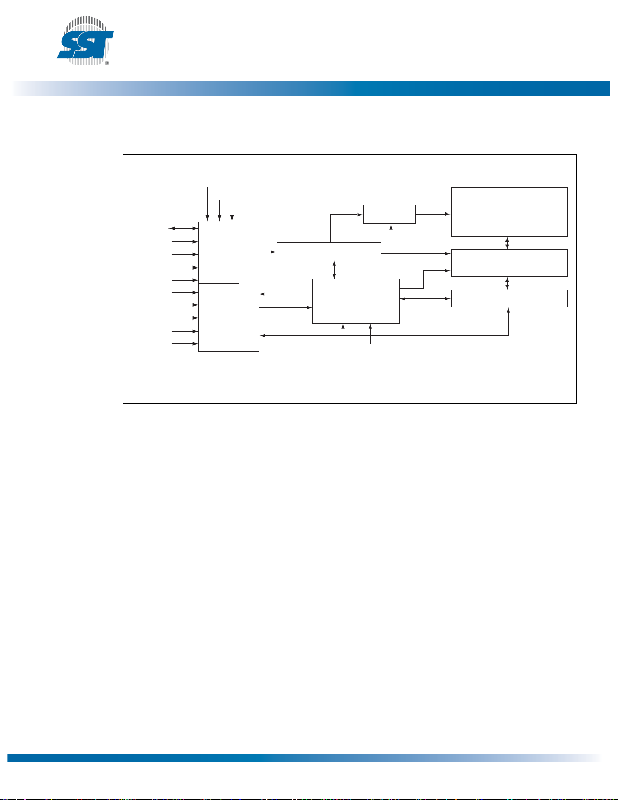
Functional Block Diagram
TBL#
WP#
FWH[3:0]
CLK
FWH4
ID[3:0]
FGPI[4:0]
R/C#
A[10:0]
DQ[7:0]
OE#
WE#
FWH
Interface
Programmer
Interface
INIT#
Address Buffers Latches
Control Logic
RST#
IC
X-Decoder
SST49LF008A
Data Sheet
SuperFlash
Memory
Y-Decoder
I/O Buffers and Data Latches
1161 B1.2
Figure 1: Functional Block Diagram
©2011 Silicon Storage Technology, Inc. DS25085A 10/11
3
8 Mbit Firmware Hub
A
Microchip Technology Company
Pin Assignments
Figure 2: Pin Assignments for 32-lead TSOP (8mm x 14mm)
NC
NC
NC
VSS(VSS)
IC (IC)
A10 (FGPI4)
R/C# (CLK)
VDD(VDD)
NC
RST# (RST#)
A9 (FGPI3)
A8 (FGPI2)
A7 (FGPI1)
A6 (FGPI0)
A5 (WP#)
A4 (TBL#)
1
2
3
4
5
6
7
8
9
10
11
12
13
14
15
16
Standard Pinout
( ) Designates FWH Mode
Top View
Die Up
32
31
30
29
28
27
26
25
24
23
22
21
20
19
18
17
1161 32-tsop P1.0
SST49LF008A
Data Sheet
OE# (INIT#)
WE# (FWH4)
VDD(VDD)
DQ7 (RES)
DQ6 (RES)
DQ5 (RES)
DQ4 (RES)
DQ3 (FWH3)
VSS(VSS)
DQ2 (FWH2)
DQ1 (FWH1)
DQ0 (FWH0)
A0 (ID0)
A1 (ID1)
A2 (ID2)
A3 (ID3)
A8 (FGPI2)
A9 (FGPI3)
4 3 21323130
A7(FGPI1)
A6 (FGPI0)
A5 (WP#)
A4 (TBL#)
A3 (ID3)
A2 (ID2)
A1 (ID1)
A0 (ID0)
DQ0 (FWH0)
( ) Designates FWH Mode
5
6
7
8
32-lead PLCC
9
10
11
12
13
14 15 16 17 18 19 20
DQ1 (FWH1)
DQ2 (FWH2)
Figure 3: Pin Assignments for 32-lead PLCC
RST# (RST#)NCV
Top View
)
SS
(V
SS
V
DQ3 (FWH3)
)
DD
(V
DD
DQ4 (RES)
R/C# (CLK)
DQ5 (RES)
A10 (FGPI4)
29
28
27
26
25
24
23
22
21
DQ6 (RES)
IC (IC)
VSS(VSS)
NC
NC
VDD(VDD)
OE# (INIT#)
WE# (FWH4)
NC
DQ7 (RES)
1161 32-plcc P2.3
©2011 Silicon Storage Technology, Inc. DS25085A 10/11
4
8 Mbit Firmware Hub
A
Microchip Technology Company
NC (NC)
IC (IC)
NC (NC)
NC (NC)
NC (NC)
NC (NC)
A10 (FGPI4)
NC (NC)
R/C# (CLK)
V
DD
NC (NC)
RST# (RST#)
NC (NC)
NC (NC)
A9 (FGPI3)
A8 (FGPI2)
A7 (FGPI1)
A6 (FGPI0)
A5 (WP#)
A4 (TBL#)
SST49LF008A
Data Sheet
1
2
3
4
5
6
7
8
9
10
11
12
13
14
15
16
17
18
19
20
Standard Pinout
Top View
Die Up
( ) Designates FWH Mode
40
39
38
37
36
35
34
33
32
31
30
29
28
27
26
25
24
23
22
21
1232 40-tsop P1.0
V
SS
V
DD
(FWH4) WE#
(INIT#) OE#
(NC) NC
(RES) DQ7
(RES) DQ6
(RES) DQ5
(RES) DQ4
(NC) NC
V
SS
V
SS
(FWH3) DQ3
(FWH2) DQ2
(FWH1) DQ1
(FWH0) DQ0
(ID0) A0
(ID1) A1
(ID2) A2
(ID3) A3
Figure 4: Pin Assignments for 40-lead TSOP
©2011 Silicon Storage Technology, Inc. DS25085A 10/11
5
8 Mbit Firmware Hub
A
Microchip Technology Company
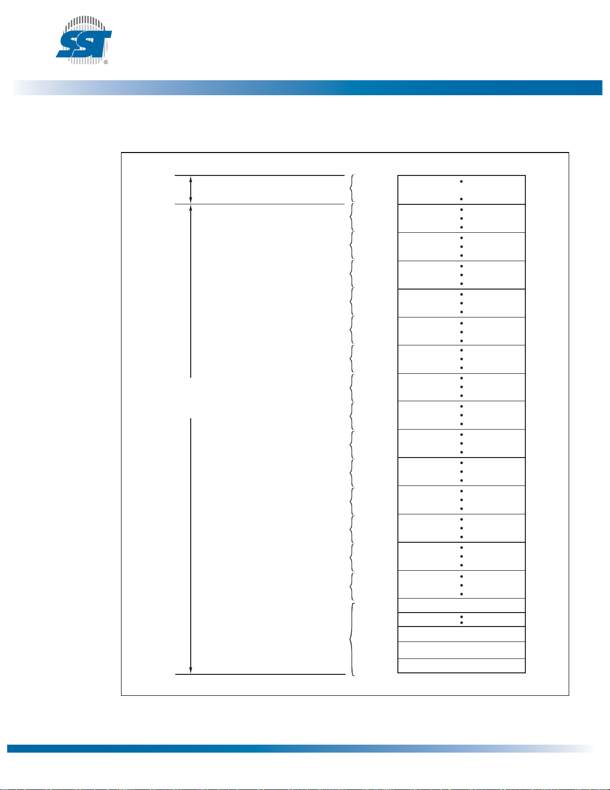
Table 1: Pin Description
Symbol Pin Name Type
A
DQ
OE# Output Enable I X To gate the data output buffers
WE# Write Enable I X To control the Write operations
IC Interface
INIT# Initialize I X This is the second reset pin for in-system use. This pin is inter-
ID[3:0] Identification
FGPI[4:0] General Pur-
TBL# Top Block Lock I X When low, prevents programming to the Boot Block sectors at top of
FWH[3:0] FWH I/Os I/O X I/O Communications
CLK Clock I X To provide a clock input to the control unit
FWH4 FWH Input I X Input Communications
RST# Reset I X X To reset the operation of the device
WP# Write Protect I X When low, prevents programming to all but the highest address-
R/C# Row/Column
RES Reserved X These pins must be left unconnected.
V
V
NC No Connection I X X Unconnected pins
SST49LF008A
Data Sheet
Interface
1
10-A0
7
Address I X Inputs for low-order addresses during Read and Write opera-
-DQ0Data I/O X To output data during Read cycles and receive input data during
I X X This pin determines which interface is operational. When held
Configuration
Pin
I X These four pins are part of the mechanism that allows multiple
Inputs
I X These individual inputs can be used for additional board flexibilpose Inputs
I X Select For the Programming interface, this pin determines whether
Select
DD
SS
1. I = Input, O = Output
Power Supply PWR X X To provide power supply (3.0-3.6V)
Ground PWR X X Circuit ground (OV reference) All VSSpins must be grounded.
FunctionsPP FWH
tions. Addresses are internally latched during a Write cycle. For
the programming interface, these addresses are latched by R/
C# and share the same pins as the high-order address inputs.
Write cycles. Data is internally latched during a Write cycle. The
outputs are in tri-state when OE# is high.
high, programmer mode is enabled and when held low, FWH
mode is enabled. This pin must be setup at power-up or before
return from reset and not change during device operation. This pin
is internally pulled- down with a resistor between 20-100 K
nally combined with the RST# pin; If this pin or RST# pin is
driven low, identical operation is exhibited.
parts to be attached to the same bus. The strapping of these
pins is used to identify the component.The boot device must
have ID[3:0]=0000 and it is recommended that all subsequent
devices should use sequential up-count strapping. These pins
are internally pulled-down with a resistor between 20-100 K
ity. The state of these pins can be read through GPI_REG register. These inputs should be at their desired state before the start
of the PCI clock cycle during which the read is attempted, and
should remain in place until the end of the Read cycle. Unused
GPI pins must not be floated.
memory. When TBL# is high it disables hardware write protection for
the top block sectors. This pin cannot be left unconnected.
able blocks. When WP# is high it disables hardware write protection for these blocks. This pin cannot be left unconnected.
the address pins are pointing to the row addresses, or to the column
addresses.
T1.4 25085
©2011 Silicon Storage Technology, Inc. DS25085A 10/11
6
8 Mbit Firmware Hub
A
Microchip Technology Company
Device Memory Map
TBL#
WP# for
Block 0 14
Block 15
Block 14
Block 13
Block 12
Block 11
Block 10
Block 9
Block 8
Block 7
Block 6
Block 5
Block 4
Block 3
Block 2
Block 1
0FFFFFH
0F0000H
0EFFFFH
0E0000H
0DFFFFH
0D0000H
0CFFFFH
0C0000H
0BFFFFH
0B0000H
0AFFFFH
0A0000H
09FFFFH
090000H
08FFFFH
080000H
07FFFFH
070000H
06FFFFH
060000H
05FFFFH
050000H
04FFFFH
040000H
03FFFFH
030000H
02FFFFH
020000H
01FFFFH
010000H
00FFFFH
SST49LF008A
Data Sheet
Boot Block
4 KByte Sector 15
Block 0
(64 KByte)
002000H
001000H
000000H
4 KByte Sector 2
4 KByte Sector 1
4 KByte Sector 0
1161 F08.0
Figure 5: Device Memory Map for SST49LF008A
©2011 Silicon Storage Technology, Inc. DS25085A 10/11
7
8 Mbit Firmware Hub
A
Microchip Technology Company
Design Considerations
SST recommends a high frequency 0.1 µF ceramic capacitor to be placed as close as possible
between VDDand VSSless than 1 cm away from the VDDpin of the device. Additionally, a low frequency 4.7 µF electrolytic capacitor from VDDto VSSshould be placed within 1 cm of the VDDpin. If you
use a socket for programming purposes add an additional 1-10 µF next to each socket.
The RST# pin must remain stable at VIHfor the entire duration of an Erase operation. WP# must
remain stable at VIHfor the entire duration of the Erase and Program operations for non-Boot Block
sectors. To write data to the top Boot Block sectors, the TBL# pin must also remain stable at VIHfor the
entire duration of the Erase and Program operations.
Product Identification
The product identification mode identifies the device as the SST49LF008A and manufacturer as SST.
Table 2: Product Identification
Manufacturer’s ID 0000H BFH FFBC0000H
Device ID
SST49LF008A 0001H 5AH FFBC0001H
Byte Data
SST49LF008A
Data Sheet
JEDEC ID
Address
Location
T2.7 25085
Mode Selection
The SST49LF008A flash memory devices can operate in two distinct interface modes: the Firmware
Hub Interface (FWH) mode and the Parallel Programming (PP) mode. The IC (Interface Configuration
pin) is used to set the interface mode selection. If the IC pin is set to logic High, the device is in PP
mode; while if the IC pin is set Low, the device is in the FWH mode. The IC selection pin must be configured prior to device operation. The IC pin is internally pulled down if the pin is not connected. In
FWH mode, the device is configured to interface with its host using Intel’s Firmware Hub proprietary
protocol. Communication between Host and the SST49LF008A occurs via the 4-bit I/O communication
signals, FWH [3:0] and the FWH4. In PP mode, the device is programmed via an 11-bit address and
an 8-bit data I/O parallel signals. The address inputs are multiplexed in row and column selected by
control signal R/C# pin. The column addresses are mapped to the higher internal addresses, and the
row addresses are mapped to the lower internal addresses. See the Device Memory Map in Figure 5
for address assignments.
©2011 Silicon Storage Technology, Inc. DS25085A 10/11
8

8 Mbit Firmware Hub
A
Microchip Technology Company
Firmware Hub (FWH) Mode
Device Operation
The FWH mode uses a 5-signal communication interface, FWH[3:0] and FWH4, to control operations
of the SST49LF008A. Operations such as Memory Read and Memory Write uses Intel FWH propriety
protocol. JEDEC Standard SDP (Software Data Protection) Byte-Program, Sector-Erase and BlockErase command sequences are incorporated into the FWH memory cycles. Chip-Erase is only available in PP Mode.
The device enters standby mode when FWH4 is high and no internal operation is in progress. The
device is in ready mode when FWH4 is low and no activity is on the FWH bus.
Firmware Hub Interface Cycles
Addresses and data are transferred to and from the SST49LF008A by a series of “fields,” where each
field contains 4 bits of data. SST49LF008A supports only single-byte Read and Write, and all fields are
one clock cycle in length. Field sequences and contents are strictly defined for Read and Write operations. Addresses in this section refer to addresses as seen from the SST49LF008A’s “point of view,”
some calculation will be required to translate these to the actual locations in the memory map (and
vice versa) if multiple memory devices are used on the bus. Tables 3 and 4 list the field sequences for
Read and Write cycles.
SST49LF008A
Data Sheet
©2011 Silicon Storage Technology, Inc. DS25085A 10/11
9

8 Mbit Firmware Hub
A
Microchip Technology Company
Table 3: FWH Read Cycle
Clock
Cycle
SST49LF008A
Data Sheet
Field
Name
1 START 1101 IN FWH4 must be active (low) for the part to respond. Only the
2 IDSEL 0000 to 1111 IN Indicates which FWH device should respond. If the to IDSEL (ID
3-9 IMADDR YYYY IN These seven clock cycles make up the 28-bit memory address.
10 IMSIZE 0000 (1 byte) IN A field of this size indicates how many bytes will be or trans-
11 TAR0 1111 IN
12 TAR1 1111 (float) Float
13 RSYNC 0000 (READY) OUT During this clock cycle, the FWH will generate a “ready-sync”
14 DATA YYYY OUT YYYY is the least-significant nibble of the least-significant data byte.
15 DATA YYYY OUT YYYY is the most-significant nibble of the least-significant data byte.
16 TAR0 1111 OUT
17 TAR1 1111 (float) Float thenINThe master (Intel ICH) resumes control of the bus during this
1. Field contents are valid on the rising edge of the present clock cycle.
Field Contents
FWH[3:0]
1
FWH[3:0]
Direction Comments
last start field (before FWH4 transitions high) should be recognized. The START field contents indicate a FWH memory
Read cycle.
select) field matches the value ID[3:0], then that particular device will
respond to the whole bus cycle.
YYYY is one nibble of the entire address. Addresses are transferred most-significant nibble first.
ferred during multi-byte operations. The SST49LF008A will only
support single-byte operation. IMSIZE=0000b
In this clock cycle, the master (Intel ICH) has driven the bus
then Float
then float to all ‘1’s and then floats the bus, prior to the next
clock cycle. This is the first part of the bus “turnaround cycle.”
The SST49LF008A takes control of the bus during this cycle.
then OUT
During the next clock cycle, it will be driving “sync data.”
(RSYNC) indicating that the least-significant nibble of the leastsignificant byte will be available during the next clock cycle.
In this clock cycle, the SST49LF008A has driven the bus to all
then Float
ones and then floats the bus prior to the next clock cycle. This
is the first part of the bus “turnaround cycle.”
cycle.
T3.3 25085
CLK
FWH4
FWH[3:0]
STR TAR RSYNCIMSIMADDRIDS DATA TAR
1161 F09.0
Figure 6: Single-Byte Read Waveforms
©2011 Silicon Storage Technology, Inc. DS25085A 10/11
10
8 Mbit Firmware Hub
A
Microchip Technology Company
Table 4: FWH Write Cycle
Clock
Cycle
SST49LF008A
Data Sheet
Field
Name
1 START 1110 IN FWH4 must be active (low) for the part to respond. Only
2 IDSEL 0000 to 1111 IN Indicates which SST49LF008A device should respond.
3-9 IMADDR YYYY IN These seven clock cycles make up the 28-bit memory
10 IMSIZE 0000 (1 byte) IN This size field indicates how many bytes will be trans-
11 DATA YYYY IN This field is the least-significant nibble of the data byte.
12 DATA YYYY IN This field is the most-significant nibble of the data byte.
13 TAR0 1111 IN then Float In this clock cycle, the master (Intel ICH) has driven the
14 TAR1 1111 (float) Float then OUT The SST49LF008A takes control of the bus during this
15 RSYNC 0000 OUT The SST49LF008A outputs the values 0000, indicating
16 TAR0 1111 OUT then Float In this clock cycle, the SST49LF008A has driven the bus
17 TAR1 1111 (float) Float then IN The master (Intel ICH) resumes control of the bus during this
1. Field contents are valid on the rising edge of the present clock cycle.
Field Contents
FWH[3:0]
1
FWH[3:0]
Direction Comments
the last start field (before FWH4 transitions high) should
be recognized. The START field contents indicate a FWH
memory Read cycle.
If the IDSEL (ID select) field matches the value
ID[3:0], then that particular device will respond to the
whole bus cycle.
address. YYYY is one nibble of the entire address.
Addresses are transferred most-significant nibble first.
ferred during multi-byte operations. The FWH only
supports single-byte writes. IMSIZE=0000b
This data is either the data to be programmed into the
flash memory or any valid flash command.
then float bus to all ‘1’s and then floats the bus prior to
the next clock cycle. This is the first part of the bus “turnaround cycle.”
cycle. During the next clock cycle it will be driving the
“sync” data.
that it has received data or a flash command.
to all then float ‘1’s and then floats the bus prior to the
next clock cycle. This is the first part of the bus “turnaround cycle.”
cycle.
T4.4 25085
CLK
FWH4
FWH[3:0]
STR DATA TARTA R
IMSIMADDRIDS
RSYNC
1161 F10.0
Figure 7: Write Waveforms
©2011 Silicon Storage Technology, Inc. DS25085A 10/11
11

8 Mbit Firmware Hub
A
Microchip Technology Company
Abort Mechanism
If FWH4 is driven low for one or more clock cycles during a FWH cycle, the cycle will be terminated
and the device will wait for the ABORT command. The host may drive the FWH[3:0] with ‘1111b’
(ABORT command) to return the device to Ready mode. If abort occurs during a Write operation, the
data may be incorrectly altered.
Response To Invalid Fields
During FWH operations, the FWH will not explicitly indicate that it has received invalid field sequences.
The response to specific invalid fields or sequences is as follows:
Address out of range:
The FWH address sequence is 7 fields long (28 bits), but only the last five address fields (20 bits) will
be decoded by SST49LF008A.
Address A22has the special function of directing reads and writes to the flash core (A22=1) or to the
register space (A22=0).
Invalid IMSIZE field:
If the FWH receives an invalid size field during a Read or Write operation, the device will reset and no
operation will be attempted. The SST49LF008A will not generate any kind of response in this situation.
Invalid-size fields for a Read/Write cycle are anything but 0000b.
SST49LF008A
Data Sheet
Device Memory Hardware Write Protection
The Top Boot Lock (TBL#) and Write Protect (WP#) pins are provided for hardware write protection of
device memory in the SST49LF008A. The TBL# pin is used to write protect 16 boot sectors (64 KByte)
at the highest flash memory address range for the SST49LF008A. WP# pin write protects the remaining sectors in the flash memory.
An active low signal at the TBL# pin prevents Program and Erase operations of the top boot sectors.
When TBL# pin is held high, write protection of the top boot sectors is then determined by the Boot
Block Locking register. The WP# pin serves the same function for the remaining sectors of the device
memory. The TBL# and WP# pins write protection functions operate independently of one another.
Both TBL# and WP# pins must be set to their required protection states prior to starting a Program or
Erase operation. A logic level change occurring at the TBL# or WP# pin during a Program or Erase
operation could cause unpredictable results. TBL# and WP# pins cannot be left unconnected.
TBL# is internally OR’ed with the top Boot Block Locking register. When TBL# is low, the top Boot
Block is hardware write protected regardless of the state of the Write-Lock bit for the Boot Block Locking register. Clearing the Write-Protect bit in the register when TBL# is low will have no functional
effect, even though the register may indicate that the block is no longer locked.
WP# is internally OR’ed with the Block Locking register. When WP# is low, the blocks are hardware
write protected regardless of the state of the Write-Lock bit for the corresponding Block Locking registers. Clearing the Write-Protect bit in any register when WP# is low will have no functional effect, even
though the register may indicate that the block is no longer locked.
©2011 Silicon Storage Technology, Inc. DS25085A 10/11
12

8 Mbit Firmware Hub
A
Microchip Technology Company
Reset
AVILon INIT# or RST# pin initiates a device reset. INIT# and RST# pins have the same function internally. It is required to drive INIT# or RST# pins low during a system reset to ensure proper CPU initialization.
During a Read operation, driving INIT# or RST# pins low deselects the device and places the output
drivers, FWH[3:0], in a high-impedance state. The reset signal must be held low for a minimal duration
of time T
operation. See Table 19, Reset Timing Parameters for more information. A device reset during an
active Program or Erase will abort the operation and memory contents may become invalid due to data
being altered or corrupted from an incomplete Erase or Program operation.
Write Operation Status Detection
The SST49LF008A device provides two software means to detect the completion of a Write (Program
or Erase) cycle, in order to optimize the system Write cycle time. The software detection includes two
status bits: Data# Polling (DQ7) and Toggle Bit (DQ6). The End-of-Write detection mode is incorporated into the FWH Read cycle. The actual completion of the nonvolatile write is asynchronous with the
system; therefore, either a Data# Polling or Toggle Bit read may be simultaneous with the completion
of the Write cycle. If this occurs, the system may possibly get an erroneous result, i.e., valid data may
appear to conflict with either DQ7or DQ6. In order to prevent spurious rejection, if an erroneous result
occurs, the software routine should include a loop to read the accessed location an additional two (2)
times. If both reads are valid, then the device has completed the Write cycle, otherwise the rejection is
valid.
SST49LF008A
A reset latency will occur if a reset procedure is performed during a Program or Erase
RSTP.
Data Sheet
Data# Polling (DQ7)
When the SST49LF008A device is in the internal Program operation, any attempt to read DQ7will produce the complement of the true data. Once the Program operation is completed, DQ7will produce
true data. Note that even though DQ7may have valid data immediately following the completion of an
internal Write operation, the remaining data outputs may still be invalid: valid data on the entire data
bus will appear in subsequent successive Read cycles after an interval of 1 µs. During internal Erase
operation, any attempt to read DQ7will produce a ‘0’. Once the internal Erase operation is completed,
DQ7will produce a ‘1’. Proper status will not be given using Data# Polling if the address is in the invalid
range.
Toggle Bit (DQ6)
During the internal Program or Erase operation, any consecutive attempts to read DQ6will produce
alternating ‘0’s and ‘1’s, i.e., toggling between 0 and 1. When the internal Program or Erase operation
is completed, the toggling will stop.
Multiple Device Selection
The four ID pins, ID[3:0], allow multiple devices to be attached to the same bus by using different ID
strapping in a system. When the SST49LF008A is used as a boot device, ID[3:0] must be strapped as
0000, all subsequent devices should use a sequential up-count strapping (i.e. 0001, 0010, 0011, etc.).
The SST49LF008A will compare the strapping values, if there is a mismatch, the device will ignore the
remainder of the cycle and go into standby mode. For further information regarding FWH device map-
©2011 Silicon Storage Technology, Inc. DS25085A 10/11
13
8 Mbit Firmware Hub
A
Microchip Technology Company
ping and paging, please refer to the Intel 82801(ICH) I/O Controller Hub documentation. Since there is
no ID support in PP Mode, to program multiple devices a stand-alone PROM programmer is recommended.
Registers
There are three types of registers available on the SST49LF008A, the General Purpose Inputs register, Block Locking registers and the JEDEC ID registers. These registers appear at their respective
address location in the 4 GByte system memory map. Unused register locations will read as 00H.
Attempts to read or write to any registers during internal Write operations will be ignored.
General Purpose Inputs Register
The GPI_REG (General Purpose Inputs Register) passes the state of FGPI[4:0] pins at power-up on
the SST49LF008A. It is recommended that the FGPI[4:0] pins are in the desired state before FWH4 is
brought low for the beginning of the bus cycle, and remain in that state until the end of the cycle. There
is no default value since this is a pass-through register. The GPI register for the boot device appears at
FFBC0100H in the 4 GByte system memory map, and will appear elsewhere if the device is not the
boot device. Register is not available for read when the device is in Erase/Program operation. See
Table 5 for the GPI_REG bits and function.
SST49LF008A
Data Sheet
Table 5: General Purpose Inputs Register
Pin #
Bit Function
7:5 Reserved - - -
4 FGPI[4]
Reads status of general
purpose input pin
3 FGPI[3]
Reads status of general
purpose input pin
2 FGPI[2]
Reads status of general
purpose input pin
1 FGPI[1]
Reads status of general
purpose input pin
0 FGPI[0]
Reads status of general
purpose input pin
32-PLCC 32-TSOP 40-TSOP
30 6 7
31115
41216
51317
61418
T5.3 25085
©2011 Silicon Storage Technology, Inc. DS25085A 10/11
14
 Loading...