

Page 1

FEATURES:
16 Megabit FlashBank Memory
SST38VF166
SST38VF16616Mb (x16) FlashBank + 64Kb E
2
Data Sheet
• Single 2.7-3.6V Read and Write Operations
• Separate Memory Banks for Code or Data
– Simultaneous Read and Write Capability
• Superior Reliability
– Endurance:
2
E
bank - 500,000 Cycles (typical)
Flash bank - 100,000 Cycles (typical)
– Greater than 100 years Data Retention
• Low Power Consumpti on
– Active Current, Read: 15 mA (typical)
– Active Current, Concurrent Read while Write:
40 mA (typical)
– Standby Current: 3 µA (typical)
– Auto Low Power Mode Current: 3 µA (typical)
• Fast Write Operation
– Flash Bank-Erase + Program: 8 sec (typical)
– Flash Block-Erase + Program: 500 ms (typical)
– Flash Sector-Erase + Program: 30 ms (typical)
2
bank Word-Write: 9 ms (typical)
– E
• Fixed Erase, Program, Write Tim es
– Remain constant after cycling
• Read Access Time
– 70 ns
• Latched Address and Data
• End-of-Write Detection
– Toggle Bit
– Data# Polling
2
• E
Bank:
– Word-Write (Auto Erase before Program)
– Sector-Erase (32 Words) + Word-Program
(same as Flash bank)
• Flash Bank: Two Small Erase Element Sizes
– 1 KWords per Sector or 32 KWords per Block
– Erase either element before Word-Program
• CMOS I/O Compatibility
• JEDEC Standard Command Set
• Packages Availab le
– 48-Pin TSOP (12mm x 20mm)
• Continuous H ardw are a n d So f tw are
Data Protection (SDP)
• A One Time Prog ram m a bl e (OTP) E
2
Sector
PRODUCT DESCRIPTION
The SST38V F16 6 cons is ts of t hre e mem ory ban ks , 2 eac h
512K x16 bits sector mode flash EEPROM plus a 4K x16
bits word alterable E
prietary, high performance SuperFlash Technology. The
SST38VF166 erases and programs with a single power
supply. The in ternal Era se /Program in the E
parent to the user. The device conforms to (proposed)
JEDEC s tanda rd pino uts f o r w ord- wid e mem ories .
The SST38VF166 device is divided into three separate
memory banks, 2 each 512K x16 Flash banks and a 4K
2
x16 E
bank. Ea ch Flas h b ank is ty pic all y use d f or pr og ram
code storage and contains 512 sectors, each of 1 KWords
or 16 blocks, each of 3 2 KWords. The Flash ban ks may
also be used to stor e data. The E
data or configuration storage and contains 128 sectors,
each of 32 words. Any bank may be used for executing
code while writing data to a different bank. Each memory
bank is cont rol led b y s epar ate B ank En ab le (BE#) l i nes .
The SST38VF166 inherently uses less energy during
Erase, Program, and Write than alternative flash technologies. The total energy consumed is a function of the
applied voltage, current, and time of application. Since for
any given voltage range, the SuperFlash technology uses
2
PROM man ufactur ed with SST’s pro-
2
bank is trans-
2
bank is typica lly used f or
less current to program and has a shorter Erase time, the
total energy consumed during any Erase, Program, or
Write operation is less than alternative flash technologies.
The Auto Low Power mode automatically reduces the
active read current to approximately the same as standby;
thus, providing an average read current of approximately 1
mA/MHz of Read cycle time.
The SuperFlash technology provides fixed Erase, Program,
and Write times, independent of the number of Erase/Program cyc les that have occurred. Therefore the system soft ware o r hardw are does not ha v e to be mo dified or de -r at ed
as is necessary with alternative flash technologies, whose
Erase and Program times increase with accumulated
Erase/Program cycles.
Device Operation
The SST38VF1 66 op erat es as two inde pendent 8-M egabi t
Word-Program, Sector-Erase flash EEPROMs with the
additional functionality of a 64 Kbit word-alterable
2
E
PROM. All banks are superimposed in the same memory address space. All three memory banks share common address lines, I/O lines, WE#, and OE#. Memory
bank selection is by bank enable. BE#1 selects the first
©2001 Silicon Storage Technology, Inc.
327-3 2/01 S71065
1
The SST logo and SuperFlash are registered trademarks of Silicon Storage Technology, Inc.
FlashBank is a trademark of Silicon Storage Technology, Inc.
These specifications are subject to change without notice.
Page 2

16 Megabit FlashBank Memory
SST38VF166
Data Sheet
Flash bank, BE#2 selects the second Flash bank, BE#3
selects the E
2
bank. WE# is used with SDP to control the
Write or Erase and Program operation in each memory
bank.
The SST38VF166 provides the added functionality of
being able to simultaneously read from one memory bank
while writing, erasing, or programming to one other memory bank. Once the internally controlled Write, Erase, or
Progr am cycle in a memory bank has commenc ed, a di ff erent memory bank can be accessed for read. Also, once
WE# and the appli cable BE# are high during the SDP load
sequence, a different bank may be accessed to read. If
multipl e bank en able s are asserted simult aneously, the ou tputs will tri-state and no new memory operations can be
initiated. Only one bank may be written, erased, or programmed at any given time. The device ID and Common
Flash Interface (CFI) functions cannot be accessed while
any bank is w riting, era si ng, or prog r ammi ng.
The Auto Low Power Mode aut omaticall y puts the device
in a near standby mode after data has b een accessed with
a valid Read operation. This reduces the I
active read
DD
current fr om typically 15m A to typically 3µA. The Auto Low
Power mode reduces the typical I
active read current to
DD
the range of 1mA/MHz of Read cycle time. The de vice e xits
the Auto Low Power Mode with any add ress transition or
control signal transi tion used to initiate another Read c yc l e,
with no access time penalty.
Flash Bank Read
The Read operation of the SST38V F166 Flash Bank is
controlled by BE#1 or BE#2 and OE#, a bank enable and
output enable both have to be low f or the system to obtain
data from the outputs. BE#1 is used for Flash bank 1
selection. When BE#1 is high, t he Flash bank 1 is deselected. BE#2 is used for Flash bank 2 selection. When
BE#2 is high, the Flash bank 2 is deselected. OE# is the
output control and is used to gate data from the output
pins. The data bus is in high impedance state when OE#
is high. Refer to the timing waveforms for fur ther details
(Figure 2 or 3).
E2 Bank Read
The Read operation of the E2 bank is controlled by BE#3
and OE#, bot h hav e t o be lo w f o r the sys tem to obtai n dat a
from the ou tputs . BE#3 is used f or E
BE#3 is high, the E
2
bank is deselected. OE # is the output
control and is used to gate data from the output pins. The
data bus is in high impedance state when OE# is high.
Refer to t he ti min g w aveforms for fu rther de tail s ( Figur e 4) .
2
bank sel ection. Wh en
Write Modes
The SST38VF166 device has separate Write modes for
2
the E
bank and Flash banks. The conventional E2PROM
Word-Write with internally timed automatic Erase before
Program is th e mo st c onvenien t and easy met hod for t he
user to alte r data in the E
2
bank with the Word-Write operation, the word being written is the only word that is altered.
Bank- or Sector -Erase plus Word-Pro gram operations m ay
also be used for the E
2
bank. For both banks of the Flash
array, the SST38VF166 offers Bank-, Block-, and SectorErase pl us W or d-Pr ogr am ope r ation s.
Write
All Write operations are initiated by first issuing the Software Da ta Pr ot ect (SDP) e nt ry seque nce f or B ank- , Blo ck -,
or Sector-Erase then Word-Program in the selected Flash
bank; or for Word-Write or for Sector-Erase and Word-Program in the E
Erase commands have a fixed duration, that will not vary
over the life of the devi ce, i.e., are i ndependent of the nu m ber of Erase/Program cycles endured.
Either Flash bank may be read during the internally controlled E
accessed to fetch instructions or data when the E
being written, erased, or programmed. Additionally, the
alternate Flash bank may be read while erasing or programming the other Flash or E
only one ban k ma y b e performing a Write oper atio n, duri ng
that ti me an y oth er bank is available fo r r ead.
The Write Status command may be used to determine if
any bank is being written, at any given time. This may be
required if the system does not use a timer or does not
monitor toggle bit or data# polling when writing a specific
bank. In order to implement the Write Status command,
address 5XXXH i n t he E
This add re ss i s out si de t he normal addre ss spa ce of t he E
bank; therefore , w ill not interfer e wit h normal reading within
2
the E
bank addres s spa ce.
The device is always in the Soft ware Data P rotected mode
for a ll Write o per ati ons in b oth t he Fl ash ba nk a nd E
Write operations are controlled by toggling WE# or BE#.
The falling edge of WE# or BE#, whichever occurs last,
latches the address. The rising edge of WE# or BE#,
whichever occurs last, latches the data and initiates the
Erase , Prog r am, or Writ e cycl e.
The SDP Erase, Program, or Write comm ands are all BE#
specific. Which ever BE# is us ed for the firs t SD P bus cyc l e
(except for Read operation with WE# high), that BE# must
be used for all subsequent SDP bus cycles, for the command to be executed. If a different BE# is pulsed during a
2
bank. Word-Write, Word-Program, and all
2
bank Write cycle, e.g., the Flash bank may be
2
bank. At any given time,
2
bank addre ss spa ce is re serv ed.
2
bank is
2
bank.
2
©2001 Silicon Storage Technology, Inc. 327-3 2/01 S71065
2
Page 3

16 Megabit FlashBank Memory
SST38VF166
Data Sheet
subsequent bus cycle, when WE# is low, in the SDP com-
mand sequence, the device will abort the attempted SDP
command and rever t to the Read mode. Note, the SDP
command sequence may be suspended by taking WE#
high. A different BE# may then be pulsed to read from
either of the banks not involved with the SDP command
sequence .
For the purposes of simplification, the following descriptions will assume WE# is toggled to initiate an Erase, Program, or Wri te . Toggli ng t he app li cab le BE# wil l ac compl is h
the same function. Note, there are separate timing diagrams to illustrate both WE# and BE# controlled Program
or Write commands.
Flash Bank Word-Program
The Flash bank Word-Program operation consists of issuing the SDP Word-Program command, initiated by forcing
BE#1 or BE#2 and WE# low, and OE# high. The words to
be programmed must be in the erased state, prior to programming. The Word-Program command programs the
desired addresses word-by-word. During the Word-Program cyc le, the addres ses are la tched b y the f alli ng edge of
WE#. The data is latched by the rising edge of WE#. See
Figure 5 or 7 for WE# or 6 and 8 for BE# controlled WordProgram cycle timing wav eforms, Table 6 for the command
sequence , and Fi gure 49 f or a flo wchart.
The Write operation has two functional cycles: the Word
Load cycle and the internal Write cycle. The Word Load
cycle consists of loading 1 word of data into the word buffer
at the completion of the SDP sequence. The internal Write
cycle consists of the write timer operation, to erase and
program the selected address. Note, the word does NOT
have to be erased prior to writing. During the Write operation, the only valid reads are Data# Polling and Toggle Bit
from the E
2
bank or normal read from either of the Flash
banks.
E2 Bank Word-Program
The E2 bank Word-Program operation consists of issuing
the SDP Word-Program command, initiated by forcing
BE#3 and WE# low and OE# high. The Word-Program
command programs the desired addresses word-by-word.
The words to be programmed must be in the er ased state ,
prior to programming, unlike the Word-Write operation.
During t he W or d-Pr ogr am c ycle , the add ress es ar e la tch ed
by the f allin g edge of WE#. The data is latched by t he rising
edge of WE#. See Figure 11 for WE# or 12 for BE#3 controlled Program cycle timing waveforms, Table 7 for the
command seq uen ce and Fi gur e 50 f o r a flow chart.
During the E
valid reads f rom the bank are Dat a# P olling and Toggle Bit.
Either Fl ash bank m ay be read .
2
bank Erase or Program operation, the only
During the Flash bank Erase or Program operation, the
only valid reads from that bank are Data# Polling and Toggle Bit . The ot her F la sh bank or t he E
2
bank may be r ead .
The specified Bank-, Block-, or Sector-Erase time is the
only ti m e r eq uired to erase. Ther e are no pr eprogram ming
or other commands or cycles required either internally or
exte rnally to er ase t he bank , b lo c k, or s ect or.
E2 Bank Word-Write
The E2 bank Word-Write operation consists of issuing the
SDP command, initiated by forcing BE#3 and WE# low,
and OE# high; followed by the Word Load cycle to the
SST38 VF1 66. The i nter nal ly co ntrol led Wr ite cy cle s tores
the data loaded in the word buffer into the E
address se lected is then eras ed and progr ammed, by inter nally controlled signals. During the Word Load cycle, the
address is latched by the falling edge of WE#. The data is
latched by the rising edge of WE#. The internal write cycle
is init iated on the risin g edge of WE#. The Write cycl e, onc e
initiated, will continue to completion, typically within 7 ms.
See Figure 9 for WE# or 10 for BE# controlled write cycle
timing w a v ef o rms, Table 7 for the command s equenc e , a nd
Figure 48 for a flowchart.
2
bank. The
The specified Bank- or Sector-Erase time is the only time
required to erase. There are no preprogramming or other
commands or cy cl es required either int ernally or externally
to eras e the ba nk or s ec tor.
Erase Operations
The Bank-Erase is initiated by a specific six-word load
sequence See Tables 6 and 7. A Bank-Erase will typically
be less th an 70 ms.
An alternative to the Bank-Erase in the Flash bank is the
Block-Erase or Sector-Erase. The Block-Erase will erase
an enti re Blo ck (3 2 KW ords ) i n ty pic ally 15 ms . The Sec tor Erase will erase an entire sector (1024 words) in typically
15 ms. The Sector-Erase provides a means to alter a single sector using the Sector-Erase and Word-Program
modes. The Sector-Erase is initiated by a specific six-word
load sequ ence , se e Table 6.
2
The E
Bank-E rase. An E
will typically erase in 7 ms. The Sector-Erase is initiated b y
a specific six-word load sequence, see Table 7. Sector- or
Bank-Erase and Word-Program is an alternative to WordWrite as a means to alter the E
bank may also use a Sector-Erase, instead of
2
bank sector consists of 32 words that
2
bank.
©2001 Silicon Storage Technology, Inc. 327-3 2/01 S71065
3
Page 4

During any Sector-, Block-, or Bank-Erase within a bank,
any other bank may be read. Du ri ng the Wor d-Write of t he
2
E
bank, eith er Fl ash ban k ma y be rea d.
Flash Bank Bank-Erase
The SST38VF166 provides a Flash Bank-Erase mode,
which allows the user to clear the Flash bank to the “1”
state. This is useful when the entire Flash must be quickly
erased.
The soft war e Fla sh B ank- Era se m ode i s ini ti ated by issui ng
the specific six-word loading sequence, as in the Software
Data Protection operation. After the loading cycle, the
device enters into an internally timed cycle. See Table 6 for
specific codes, Figure 13 or 16 for the timing waveform,
and Figure 44 f o r a f lo wch art.
Flash Bank Block-Erase
The SST38VF166 provides a Block-Erase mode, which
allows the user to clear any block in the Flash bank to the
“1” state.
The software Block-Erase mode is initiated by issuing the
specific six-word loading sequence, as in the Software
Data Protect operation. After the loading cycle, the device
enters int o an i nternally time d Er as e cycle. See Table 6 for
specific codes, Figure 14 or 17 for the timing waveform,
and Figure 45 for a flowchart. During the Erase operation,
the only valid reads are Data# Polling and Toggle Bit from
the sel ect ed bank , ot her ban ks ma y per f orm normal read.
Flash Bank Sector-Erase
The SST38VF166 provides a Sector-Erase mode, which
allows the user to c lear any sector in the Flash bank to the
“1” state.
The softw are Sector-E rase mode is initiated by issuing the
specific six-word loading sequence, as in the Software
Data Protect operation. After the loading cycle, the device
enters int o an i nternally time d Er as e cycle. See Table 6 for
specific codes, Figure 15 or 18 for the timing waveform,
and Figure 47 for a flowchart. During the Erase operation,
the only valid reads are Data# Polling and Toggle Bit from
the sel ect ed bank , ot her ban ks ma y per f orm normal read.
E2 Bank Bank-Erase
The SST38VF166 prov ides a E2 Bank-Erase mode, wh i ch
allows the user to clear the E
useful when the entire E
2
The E
bank Bank-Erase command is disabled if the E
bank O TP op tion i s ena b led .
2
bank to the “1” state. This is
2
bank must be quickly erased.
16 Megabit FlashBank Memory
SST38VF166
2
Bank-Eras e mod e is init ia ted b y i ssui ng the s pe cifi c
The E
six-word loading sequence, as in the Software Data Protection operati on. Af t er the loading cycle, t he device enters
into an internally timed cycle. See Table 7 for specific
codes, Fig ure 19 f or the ti ming w a v e f orm, and F i gure 4 4 f o r
a fl owchart.
E2 Bank Sector-Erase
The SST38VF166 provides a Sector-Erase mode, which
allo ws the user to clear any sector in the E
state . The softwar e Sec t or-Erase mo de i s ini tiated b y issuing the specific six-word loading sequence, as in the Software Data Protect operation. After the loading cycle, the
device enters into an internally timed. See Tables 6 and 7
for specific codes, Figure 20 for the timing waveform, and
Figure 46 for a flowchart. During the Erase operation, the
only valid reads are Data# Polling and Toggle Bit in the E
bank or norma l re ad fr om eit her of the Flas h ban ks .
Write Operation Status Detection
The SST38VF166 provides two software means to detect
the completion of a E
cycle, in or der to op t i m i z e the sys tem Write c ycle time. The
software detection includes two status bits: Data# Polling
(DQ
) and Toggle Bit (DQ6). The End-of-Write Detection
7
mode is enabled after the rising edge of WE#, which initiates the internal Write, Erase, or Program cycle.
The actual completion of the nonvolatile write is asynchronous with the system; therefore, either a Data# Polling or
Toggle Bit read may be simultaneous with the completion
of the Write c ycle. If this occ urs, the system wil l possib ly get
an erroneous result, i.e. valid data may appear to conflict
with either DQ
or DQ6. In order to pre v en t spuri ous dev ic e
7
rejecti on, if a n e rrone ous r es ult o ccur s, th e sof tw are r out ine
should include a loop to read the accessed location an
additional two (2) times. If both reads are valid, then the
device ha s completed the Write cycle, oth erwise th e rejection is valid.
Additi onally, a Write Status rea d may be executed to determine if any bank has an Erase, Program, or Write operation in progress. A Write Status read may be used when,
for an y reason, the syste m may ha ve lost trac k of the statu s
of a Write, Erase, or Program operation in any bank.
Although nor mally, a Word-Write, Word-Program, Se ctorErase, or Block-Erase will be completed prior to recovery
from a system reset, if a Bank-Erase was initiated prior to
the reset, the system may need to verify the Bank-Erase is
no longer in progress. Note, a Bank-Erase will not be per-
2
formed on the bank containing the boot code, so there will
2
bank or a Flash bank Program
2
Data Sheet
bank to t he “1”
2
©2001 Silicon Storage Technology, Inc. 327-3 2/01 S71065
4
Page 5

16 Megabit FlashBank Memory
SST38VF166
Data Sheet
be no is sue when recoveri ng from the syst em res et. See
Table 6 or 7 f or the s pecific codes and Figure 40 for a timing
waveform.
There is no provision to abort an Erase, Program, or Write
operation, once initiated. For the SST SuperFlash technology, the associated Erase, Program, and Write times are
so fast, relative to syste m res et tim es, ther e is n o value in
aborting the operation. Note, reads can always occur from
any bank no t per f orming an E ras e, Prog r am, o r W rite op eration.
Should the system reset, while a Block- or Sector-Erase or
Word-Pro gram is in progre ss in the ban k where the bo ot
code is stored, the system must wait for the completion of
the operation before reading that bank. Since the maximum time the system would have to wait is 25 ms (for a
Block-Erase), the system ability to read the boot code
would no t be af f ect ed.
Data# Polling (DQ7) - Flash Bank
When the SST38VF166 is in the internal Flash bank Program cycle, any attempt to read DQ
of the last word
7
loaded during the Flash bank Word Load cycle will receive
the complemen t of the true data. Once th e Write cycle is
completed, DQ
will show true data. The device is then
7
ready for the next operation. See Figure 21 or 22 for the
Flash bank Data Polling timing waveforms and Figure 51
for a f lo w chart.
Data# Polling (DQ7) - E2 Bank
When the SST38VF166 is in the internal E2 bank Write
cycle, an y atte mpt to read DQ
ing the E
2
bank Word Load c ycle w ill re ceive th e comp le-
of the last word lo aded dur-
7
ment of the true data. Once the Write cycle is completed,
DQ
will show true data. The device is then ready for the
7
next operat ion. See Figure 23 for E
2
bank Da t a Polling tim-
ing wa v ef o rms and Fig ur e 51 f o r a flo w chart.
Toggle Bit (DQ6) - Flash Bank
During th e Flash ban k internal Writ e cycle , any c onsecut ive
attempts to r ead DQ
i.e. t oggling between 0 an d 1. When the Write cycle is complete d, the togg ling wil l stop. The devi ce is then ready for
the ne xt o per a tion. See Figu re 24 or 25 for Flash bank Toggle Bit timi ng wa v ef o rms and Fi gur e 51 f or a fl o wchart.
will produce alternating 0s and 1s,
6
Toggle Bit (DQ6) - E2 Bank
During the E2 bank internal Write cycle, any consecutive
attempts to r ead DQ
will produce alternating 0s and 1s,
6
i.e. t oggling between 0 an d 1. When the Write cycle is complete d, the togg ling wi ll stop. The dev ice is then ready for
the next operation. See Figure 26 for E
2
bank Toggle Bit
timin g wa v ef orm s and F ig ure 51 for a flowchart.
Data Protection
The SST38VF166 provides both hardware and software
feat ures to pr otec t non v ol at ile da ta f ro m inadv erten t writ es .
Hardware Data Protection
Noise/Gli t ch Protecti on: A WE# pulse of less than 5 ns will
not initiate a Write cycle.
Power Up/Down Detection: The Write operation is
V
DD
inhibi ted w hen V
Write Inhi bi t Mod e:
is less th an 1.5 v olt s.
DD
Forci ng OE# lo w, BE#1 and BE#2 high,
or WE# high will inhibit the Write operation to the Flash
bank. Forcing OE # l ow, BE#3 high, or WE# high will inhibi t
the Write operati o n to the E
2
bank. This prevents inadvert-
ent writes duri ng po wer -up or po wer -d own.
A One Time Programmable E2 Sector
The first sector of the E2 bank offers the option of OTP
(One Time Programmable) prevention of write for the first
sector, i.e., addresses A
to A13 are “0” (0000 H to 001FH).
5
Once the OTP software instruction is executed, no Write,
Erase , or Progr am oper ati on can be per forme d on these 32
words . This is permanent and non- re vers ibl e. Addi tional ly, if
the OTP prevention is enabled, the Bank-Erase for the E
bank will not function. See Table 7 for specific codes and
Figure 39 for a timing waveform.
Software Data Protection (SDP)
The SST38V F16 6 p rov ide s t he JE DEC appr ov ed Sof tw are
Data Protection scheme as a requirement for initiating a
Write, E rase, or Program operation. Wi th this scheme, any
Write operation requires the inclusion of a series of three
word-load operations to precede the Word-Write or WordProgram operat i on. The three-word load sequen ce is used
to initiate the Write or Program cycle, providing optimal protection from inadver tent Write operations, e.g., during the
system power-up or power-down. The six-word sequence
is required to initiate any Bank-, Block-, or Sector-Erase
operation.
2
©2001 Silicon Storage Technology, Inc. 327-3 2/01 S71065
5
Page 6
16 Megabit FlashBank Memory
SST38VF166
Data Sheet
The requirements for JEDEC compliant SDP are in byte
format. The SST38VF166 is organized by word; therefore,
the cont ents o f DQ
to DQ15 are “Don ’t Care” durin g any
8
SDP (3-w ord o r 6- wor d) com mand sequen ce .
During the SDP load command sequence, the SDP load
cycle is suspended when WE# is high. This means a read
may occur to any other bank during the SDP load
sequence .
The SDP load sequence is bank specific, i.e., the same
BE# must be low for each bus cycle. If the command
sequence is aborted, e.g., a different BE# is brought low
(except for Read operation with WE# high), an incorrect
address is loaded, or incorrect data is loaded, the device
will return to the Read mode within T
of executi on of the
RC
load err or.
Concurrent Read and Write Operations
The SST38VF166 provides the unique benefit of being
able to read any bank, while simultaneously writing, erasing, or prog ra mming on e othe r bank. Thi s all ow s da ta a lter ation cod e t o be executed from one ba nk , whil e al te ring t he
data in another bank. The following table lists all valid
states.
TABLE 1: C
Flash Bank 1 Flash Bank 2 E2 Bank
Read No Operation Write
Read Write No Operation
Write Read No Operation
No Operation Read Write
Write No Operation Read
No Operation Write Read
Note: For the purposes of this table, write means to Word-Write;
Block-, Sector-, or Chi p-Erase; or Word-Program as applicable t o the appropriate bank.
ONCURRENT READ/WRITE STATE
T1.0 327
Product Identif icat ion
The produ ct ide nti fic atio n mode iden ti fies the device manufact urer as SST and prov i des a cod e t o identi f y each ban k.
The manufacturer ID is the same for each bank; however,
each bank has a se para te device ID . E ach b ank i s in div idu ally accessed using the applicable BE# and a software
command. Users may wish to use the device ID operation
to identify the write algorithm requirements for each bank.
For de tai ls , see Tab le 6 or 7 f or sof tw are ope r ation and Fi gures 27, 2 8, or 29 f or ti ming wa v eforms.
TABLE 2: PRODUCT IDENTIFICATION
Address Data
Manufacturer’s ID 0000H 00BFH
Device ID
Flash Bank 1 0001H 2791H
Flash Bank 2 0001H 2792H
2
Bank 0001H 2793H
E
T2.1 327
Device IDs are unique to each bank. Should a chip ID be
required, any of the bank IDs may be used as the chip ID.
While in the read softw are ID mode or CFI mo de, no othe r
operati on is all ow ed unt il af ter e x it ing th ese modes .
Product Identification Mode Exit
In order to return to the standard Read mode, the Product
Identification mode must be exited. Exit is accomplished by
issuing the Software ID exit command, which returns the
device to normal operation. This command may also be
used to reset the device to the Read mode after any inadvertent transient condition that apparently causes the
device to behave abnormally, e.g., not read correctly. For
details, see Tab le 6 or 7 for software o peration and Figures
30, 31, or 32 f o r ti min g wa v e f orms .
SST does not recommend that any two of the bank enable
signals BE#1, BE#2 o r BE#3 be simu lt aneous ly asse rted.
The device will ignore all SDP commands and toggling of
WE# when an Erase, Program, or Write operation is in
progress. Note, both Product Identification and the Common Fl ash I nt erfac e ent r y co mm an ds use SDP ; the re fore,
these commands will also be ignored while an Erase, Program, or Writ e op erat io n is i n prog re ss .
©2001 Silicon Storage Technology, Inc. 327-3 2/01 S71065
6
Page 7
16 Megabit FlashBank Memory
SST38VF166
Data Sheet
Common Flash Interface (CFI)
The SST38VF166 also contains the CFI information in
each b ank, to desc ribe the char a cte risti cs of that ba nk. S ee
Tables 8 through 16 for the CFI contents for each bank.
Both flash banks use the same infor mation, as each bank
operates the same. The E
inf ormat ion f or tha t bank.
In order to obtain the CFI information, the CFI memory
space is accessed by using the CFI entry command. For
details, see Tab le 6 or 7 for software o peration and Figures
33, 34, or 35 f o r ti min g wa v e f orms .
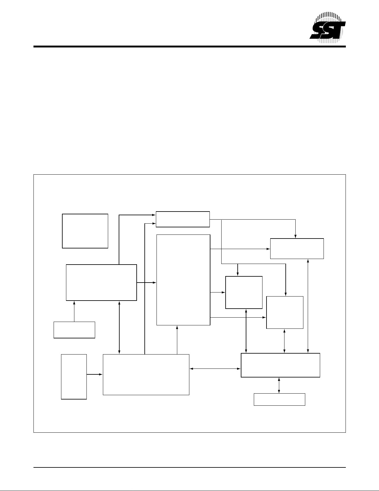
FUNCTIONAL BLOCK DIAGRAM
Charge
Pump &
Vref.
2
bank contains the applicable
Y - Decoder
CFI Mode Exit
In order to return to the standard Read mode, the CFI
mode must be exited. Exit is accomplished by issuing the
CFI exit command, which returns the device to normal
operation. This command may also be used to reset the
device to the Read mode after any inadver tent transient
condition that apparently causes the device to behave
abnormall y, e.g., not read correc tly. For deta i l s , see Table 6
or 7 for softwa re oper ation an d Figur es 36, 37, or 38 for timing wav efo rms.
CFI is specified for byte wide information. Since the
SST38VF166 is organized word wide, the first byte (2 nibbles ) of ea ch CFI wo rd is a lw a ys 00H.
4K x 16
2
Bank
E
Address Buffer
and Latches
A18 - A
0
OE#
BE#1
BE#2
BE#3
WE#
Control Logic
X - Decoder
512K x 16
Flash
Bank 1
512K x 16
Flash
Bank 2
I/O Buffers and
Data Latches
DQ15 - DQ
0
327 ILL F02.1
©2001 Silicon Storage Technology, Inc. 327-3 2/01 S71065
7
Page 8
16 Megabit FlashBank Memory
SST38VF166
Data Sheet
A15
A14
A13
A12
A11
A10
NC
NC
WE#
NC
BE#2
NC
BE#3
A18
A17
1
2
3
4
5
A9
A8
A7
A6
A5
A4
A3
A2
A1
6
7
8
9
10
11
12
13
14
15
16
17
18
19
20
21
22
23
24
Standard Pinout
T op Vie w
Die Up
48
47
46
45
44
43
42
41
40
39
38
37
36
35
34
33
32
31
30
29
28
27
26
25
A16
NC
V
SS
DQ15
DQ7
DQ14
DQ6
DQ13
DQ5
DQ12
DQ4
V
DD
DQ11
DQ3
DQ10
DQ2
DQ9
DQ1
DQ8
DQ0
OE#
V
SS
BE#1
A0
327 ILL F01b.5
FIGURE 1: P IN ASSIGNMENTS FOR 48-PIN TSOP (12MM X 20MM)
TABLE 3: P
Symbol Name Functions
A
18-A0
A
11-A0
A
18-A15
A
18-A10
A
11-A5
-DQ0Data Input/ou tput To output data during Read cycles and recei ve input data during Write cycl es.
DQ
15
OE# Output Enable To gate the data output buffers
WE# Write Enable 1 To control the Write, Erase, or Pro gram operations
V
DD
V
SS
NC No Connect Unconnected pins
IN DESCRIPTION
Flash Bank Addresses To provide Flash Bank addresses
E2 Bank Addresses To provide E2 Bank addresses
Flash Bank Block Addresses To select a Flash Bank Block for erase
Flash Bank Sector Addresses To select a Flash Bank Sector for er ase
E2 Bank Sector Addresses To select an E2 Bank Sector for erase
Data is internally latched during a Write cycle.
The outputs are in tri-state when OE# is high or BE#1, BE#2, and BE#3 are high.
Po wer Supply To provide 2.7-3.6V power supply
Ground
T3.4 327
©2001 Silicon Storage Technology, Inc. 327-3 2/01 S71065
8
Page 9
16 Megabit FlashBank Memory
SST38VF166
Data Sheet
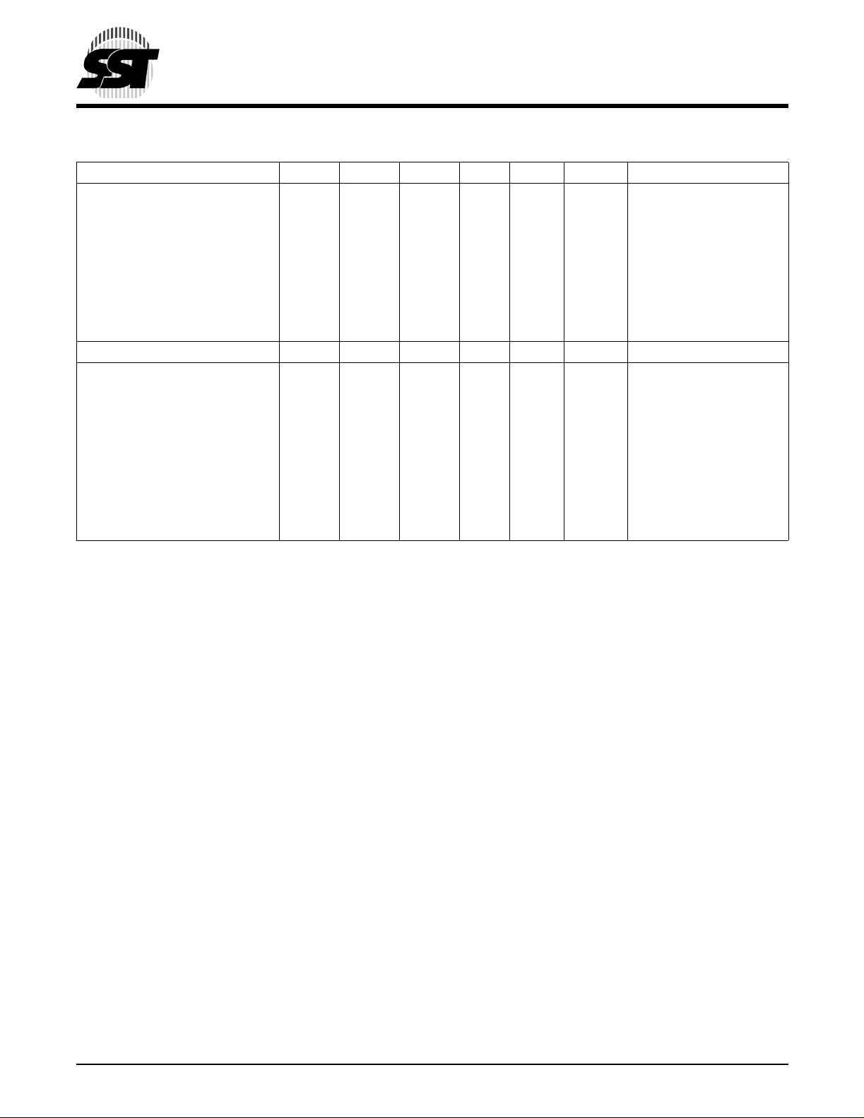
TABLE 4: OPERATION MODES SELECTION FOR FLASH BANK
Array Operation Mode BE#1 BE#2 BE#3 OE# WE# DQ Address
Read
Flash Bank 1 V
Flash Bank 2 V
IL
IH
V
IH
V
IL
Block-Erase
Flash Bank 1 V
Flash Bank 2 V
IL
IH
V
IH
V
IL
Sector-Erase
Flash Bank 1 V
Flash Bank 2 V
IL
IH
V
IH
V
IL
Program
Flash Bank 1 V
Flash Bank 2 V
Standby V
IL
IH
IH
V
IH
V
IL
V
IH
Write Inhibit
Flash Bank 1 V
IH
Flash Bank 2 X V
XXVILV
IH
Flash Bank-Erase
Flash Bank 1 V
Flash Bank 2 V
IL
IH
V
IH
V
IL
Status Operation Mode BE#1 BE#2 BE#3 OE# WE# DQ Address
Write Status Read V
Illegal State V
Illegal State V
Illegal State V
IH
IL
IL
IL
Illegal State X V
V
IH
V
IL
V
IL
XVILX X High Z X
IL
Product Identification
Flash Bank 1 V
Flash Bank 2 V
IL
IH
V
IH
V
IL
Common Flash Interface
Flash Bank 1 V
Flash Bank 2 V
1. If Flash Bank 1 is writing, DQ1 is low. If Flash Bank 2 is writing, DQ2 is low. If E2 Bank is writing, DQ3 is low.
2. Entering an illegal state during an Erase, Program, or Write operation will not affect the operation, i.e., the erase, pr ogram, or write
will continue to normal completion.
IL
IH
V
IH
V
IL
V
IH
V
IH
V
IH
V
IH
V
IH
V
IH
V
IH
V
IH
V
IH
XVILV
V
IH
V
IH
V
IL
V
IL
V
IL
V
IL
V
IH
V
IH
V
IH
V
IH
V
IH
V
IH
V
D
IH
OUT
V
D
IH
OUT
V
D
IL
IN
V
D
IL
IN
V
D
IL
IN
V
D
IL
IN
V
D
IL
IN
V
D
IL
IN
X X High Z X
XX
IH
XX
IH
V
IH
V
IH
V
IL
V
D
IL
IN
V
D
IL
IN
V
IH
1
D
OUT
X X High Z X
X X X High Z X
V
IL
V
IH
V
IH
V
IH
V
IH
X X High Z X
V
IL
V
IL
V
IL
V
IL
V
D
IH
OUT
V
D
IH
OUT
V
D
IH
OUT
V
D
IH
OUT
A
IN
A
IN
See Tables 6 and 7
See Tables 6 and 7
See Tables 6 and 7
See Tables 6 and 7
See Tables 6 and 7
See Tables 6 and 7
See Tables 6 and 7
See Tables 6 and 7
5XXXXH
2
2
2
2
See Tables 6 and 7
See Tables 6 and 7
See Tables 6 and 7
See Tables 6 and 7
T4.5 327
©2001 Silicon Storage Technology, Inc. 327-3 2/01 S71065
9
Page 10
16 Megabit FlashBank Memory
SST38VF166
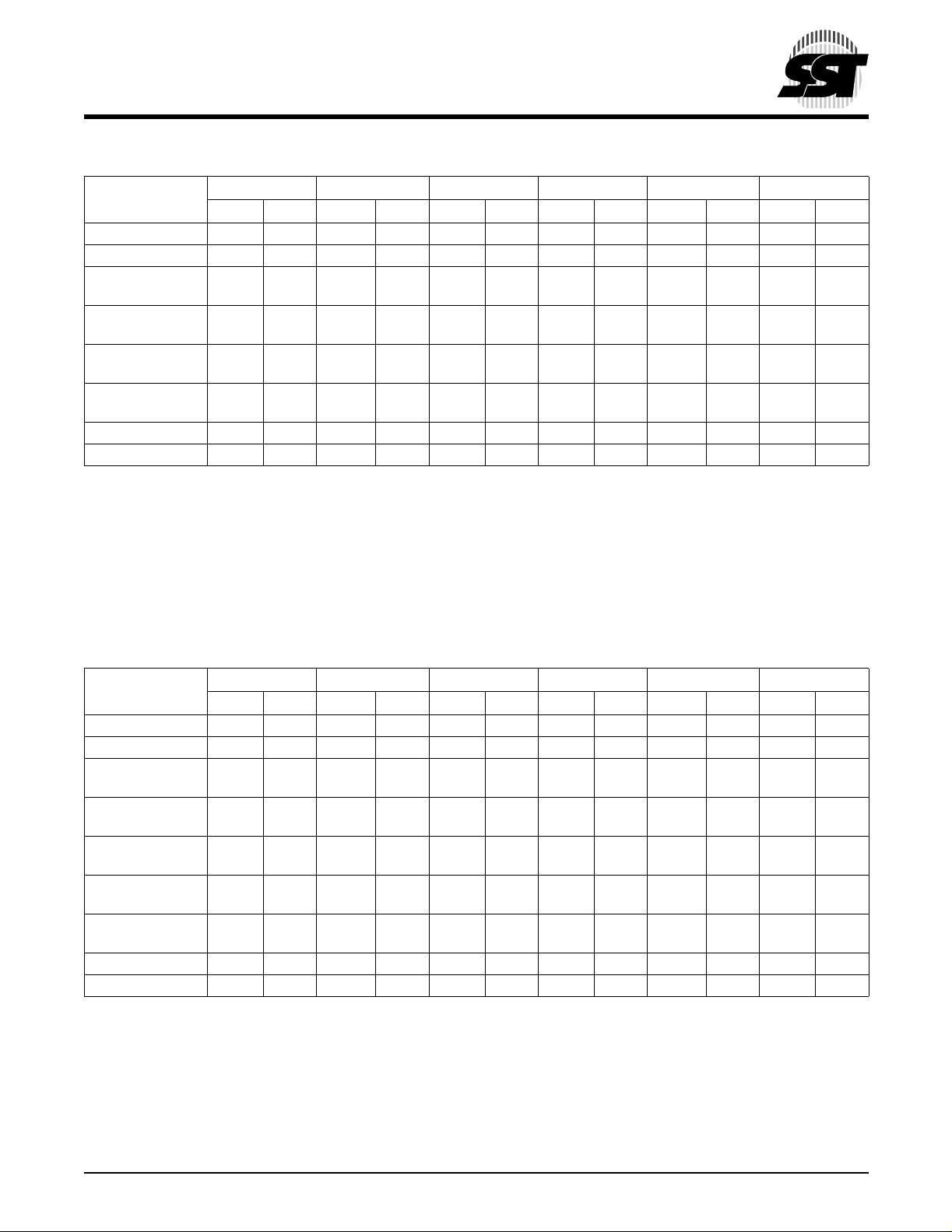
TABLE 5: OPERATION MODES SELECTION FOR E2 BANK
Read Operation Mode BE#1 BE#2 BE#3 OE# WE# DQ Address
2
Read E
Bank V
Write E2 Bank V
2
Sector-Erase E
Program E
Bank V
2
Bank V
Standby V
2
Write Inhibit E
Erase E
OTP Enable E
Bank X X V
2
Bank V
2
Bank V
IH
IH
IH
IH
IH
IH
IH
V
IH
V
IH
V
IH
V
IH
V
IH
V
IH
V
IH
V
IL
V
IL
V
IL
V
IL
V
IH
IH
V
IL
V
IL
V
IL
V
IH
V
IH
V
IH
V
IH
V
IL
V
IL
V
IL
XXDINSee Tables 6 and 7
V
IL
V
IH
V
IH
V
IH
V
IL
V
IL
Status Operation Mode BE#1 BE#2 BE#3 OE# WE# DQ Address
Write Status Read V
Illegal State V
Illegal State V
Illegal State V
IH
IL
IL
IL
Illegal State X V
V
IH
V
IL
V
IL
XVILX X High Z X
IL
V
IL
V
IL
V
IL
V
IH
X X High Z X
X X X High Z X
V
IL
X X High Z X
Product Identification
2
Bank V
E
IH
V
IH
V
IL
V
IL
V
IH
Common Flash Interface
2
Bank V
E
1. A11-A0 are v alid addresses; A15-A12 are “Don’t Care”; A18-A16 cannot be 5H
2. If Flash Bank 1 is writing, DQ
3. Entering an illegal state during an Erase, Program, or Write operation will not affect the operation, i.e., the erase, pr ogram, or write
will continue to normal completion.
is low. If Flash Bank 2 is writing, DQ2 is low. If E2 Bank is writing, DQ3 is low.
1
IH
V
IH
V
IL
V
IL
V
IH
1
D
OUT
D
IN
D
IN
D
IN
High Z X
D
IN
D
IN
2
D
OUT
D
OUT
D
OUT
See Tables 6 and 7
See Tables 6 and 7
See Tables 6 and 7
See Tables 6 and 7
See Tables 6 and 7
5XXXXH
3
3
3
3
See Tables 6 and 7
See Tables 6 and 7
Data Sheet
T5.6 327
©2001 Silicon Storage Technology, Inc. 327-3 2/01 S71065
10
Page 11
16 Megabit FlashBank Memory
SST38VF166
Data Sheet
TABLE 6: SOFTWARE COMMAND SEQUENCE FOR FLASH BANKS
1st Bus Cycle 2nd Bus Cycle 3rd Bus Cycle 4th Bus Cycle 5th Bus Cycle 6th Bus Cycle
Command Code
Software ID Entry 5555H AAH 2AAAH 55H 5555H 90H
Software ID Exit 55 55H AAH 2AAAH 55H 5555H F0H
Flash Bank
Word-Program
Flash Bank
Sector-Erase
Flash Bank
Block-Erase
Flash Bank
Bank-Erase
CFI Entry 5555H AAH 2AAAH 55H 5555H 98H
CFI Exit 5555H AAH 2AAAH 55H 5555H F0H
1. Command Code Address format A14-A0 (Hex), Addresses > A14 are “Don’t Care” for Com m and sequen c es
2. Data format DQ
3. With A
4. The device does not remain in Software Product ID Mode or CFI Mode if powered down.
5. WA = Word addre ss
6. SA = Sector address
7. There is a sepa rate CFI for each bank. S ee Tables 8 through 16
14-A1
BA = Blo ck address
Addr1Data2Addr1Data2Addr1Data2Addr1Data2Addr1Data2Addr1Data
3
4
5555H AAH 2AAAH 55H 5555H A0H WA
5
Data
In
5555H AAH 2AAAH 55H 5555H 80H 5555H AAH 2AAAH 55H SA
5555H AAH 2AAAH 55H 5555H 80H 5555H AAH 2AAAH 55H BA
5555H AAH 2AAAH 55H 5555H 80H 5555H AAH 2AAAH 55H 5555H 10H
7
4
-DQ0 (Hex), DQ15 - DQ8 are “Don’t Care”
7
= 0; SST Manufacturer’s ID = 00BFH, is read with A0 = 0
SST38VF166 Device ID = 2791H, 2 792H, and 2793H is read with A
= 1 for the applicable BE# active
0
2
6
30H
6
50H
T6.4 327
TABLE 7: SOFTWARE COMMAND SEQUENCE FOR E2 BANKS
1st Bus Cycle 2nd Bus Cycle 3rd Bus Cycle 4th Bus Cycle 5th Bus Cycle 6th Bus Cycle
Command Code
Addr
1
Software ID Entry 5555H AAH 2AAAH 55H 5555H 90H
Software ID Exit 55 55H AAH 2AAAH 55H 5555H F0H
E2 Bank
5555H AAH 2AAAH 55H 5555H A0H WA
Word-Write
2
E
Bank
5555H AAH 2AAAH 55H 5555H A5H WA
Word-Program
2
E
Bank
5555H AAH 2AAAH 55H 5555H 80H 5555H AAH 2AAAH 55H SA
Sector-Erase
2
E
Bank
5555H AAH 2AAAH 55H 5555H 80H 5555H AAH 2AAAH 55H 5555H 10H
Bank-Erase
2
E
Bank
5555H AAH 2AAAH 55H 5555H 80H 5555H AAH 2AAAH 55H 5555H 70H
OTP Enable
CFI Entry 5555H AAH 2AAAH 55H 5555H 98H
CFI Exit 5555H AAH 2AAAH 55H 5555H F0H
1. Command Code Address format A14-A0 (Hex), Addresses > A14 are “Don’t Care” for Com m and sequen c es
2. Data format DQ7 -DQ0 (Hex), DQ15 - DQ8 are “Don’t Care”
3. With A14-A1 = 0; SST Manufacturer’s ID = 00BFH, is read with A0 = 0
4. The device does not remain in Software Product ID Mode or CFI Mode if powered down.
5. WA = Word addre ss
6. SA = Sector address
7. There is a sepa rate CFI for each bank. S ee Tables 8 through 16
SST38VF166 Device ID = 2791H, 2 792H, and 2793H is read with A
Data
2
Addr1Data2Addr1Data2Addr1Data2Addr1Data2Addr1Data
3
4
5
Data
In
5
Data
In
7
4
= 1 for the applicable BE# active
0
2
6
30H
T7.4 327
©2001 Silicon Storage Technology, Inc. 327-3 2/01 S71065
11
Page 12
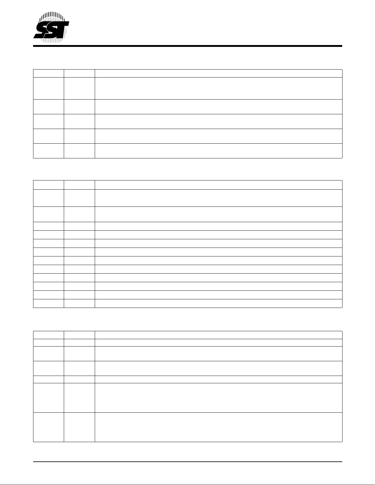
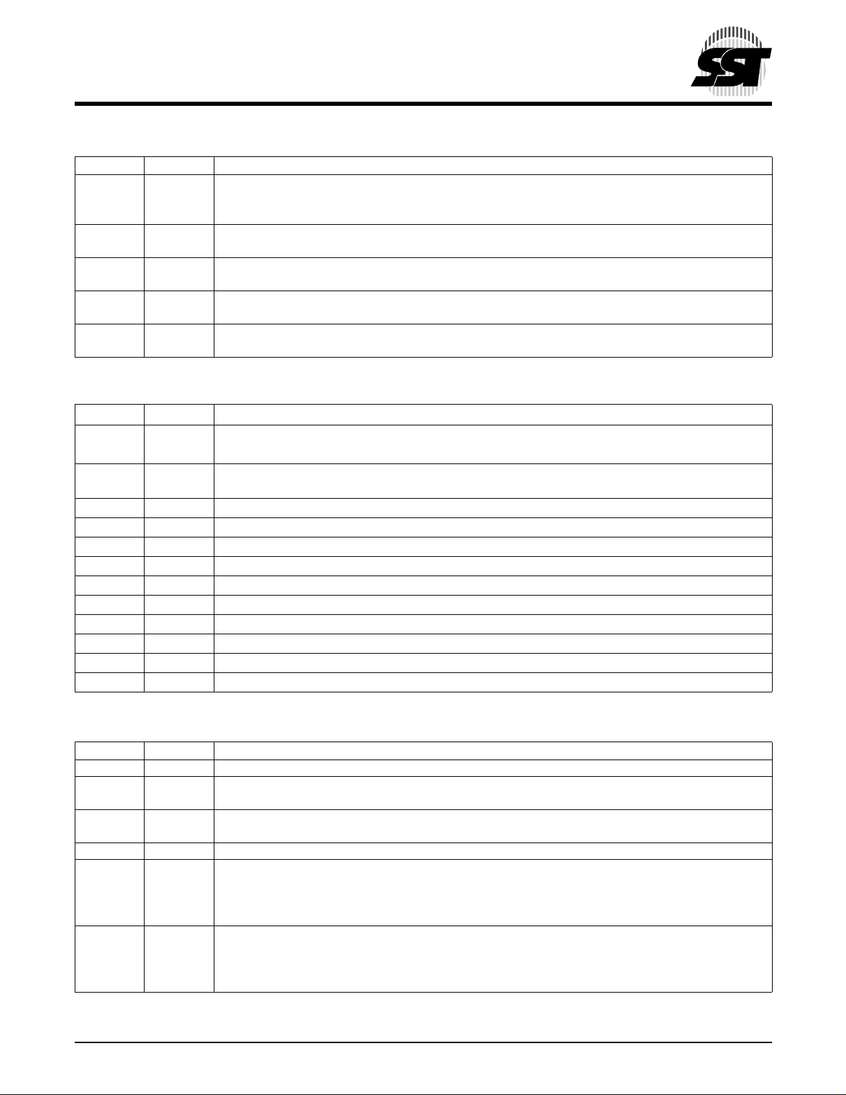
TABLE 8 : CFI QUERY IDENTIFIC ATION STRING FOR FLASH BANK 1
Address Data Data
10H 0051H Query Unique ASCII string “QRY”
11H 0052H
12H 0059H
13H 0001H Primary OEM command set (JEP-137)
14H 0008H
15H 0000H Address for Primary Extended Table (00H = none exist s)
16H 0000H
17H 0000H Alternate OEM command set (00H = none exists)
18H 0000H
19H 0000H Address for Alternate OEM extended Table (00H = none exits)
1AH 0000H
TABLE 9: SYSTEM INTERFACE INFORMATION FOR FLASH BANK 1
Address Data Data
1BH 0027H V
1CH 0036H V
1DH 0000H V
1EH 0000H V
1FH 0004H Ty pical time out for Word-Program 2
20H 0000H T ypical time out for min. size Page-Write 2
21H 0004H T ypical time out f or individual Sector-Erase 2
22H 0006H T ypical time out for Bank-Erase 2
23H 0001H Maximum time out for Word-Program 2
24H 0000H Maximum time out for Page-Write 2
25H 0001H Maximum time out for individual Sector-Erase 2
26H 0001H Maximum time out for Chip-Erase 2
Min (Program/Erase)
DD
-DQ4: Volts, DQ3-DQ0: 100 millivolts
DQ
7
Max (Program/E rase)
DD
DQ
-DQ4: Volts, DQ3-DQ0: 100 millivolts
7
min. (00H = no VPP pin)
PP
max. (00H = no VPP pin)
PP
N
µs
N
µs (00H = not supported)
N
ms
N
ms
N
times typical
N
times typical (00H = not supported)
N
times typical
N
times typical
16 Megabit FlashBank Memory
SST38VF166
Data Sheet
T8.2 327
T9.7 327
TABLE 10: DEVICE GEOMETRY INFORMATION FOR FLASH BANK 1
Address Data Data
27H 0014H Bank size = 2
28H 0001H Flash Bank Device Interface description (Refer to CFI JESD-68) (x1 6 asynchronous)
29H 0000H
2AH 0000H M aximum number of bytes in Page-Write = 2
2BH 0000H
2CH 0002H Number of Erase Block Regions within device
2DH 00FFH Erase Block Region 1 Information (Sector)
2EH 0001H (Refer to the CFI specification or JESD-68)
2FH 0008H y = 511 + 1 = 512 sectors (01FFH = 511)
30H 0000H z = 2 KBytes/sector = 8 x 256 Bytes
31H 000FH Erase Block Region 2 Information (Block)
32H 0000H (Refer to the CFI specification or JESD-68)
33H 0000H y = 15 + 1 = 16 blocks
34H 0001H z = 64 KBytes/block = 256 x 256 Bytes (0100H = 64K)
©2001 Silicon Storage Technology, Inc. 327-3 2/01 S71065
N
Byte (14H > 220 = 1 MByte = 8 Mbits)
N
(00H = not supported)
12
T10.5 327
Page 13
16 Megabit FlashBank Memory
SST38VF166
Data Sheet
TABLE 11: CFI QUERY IDENTIFICATION S TRING FOR FLASH BANK 2
Address Data Data
10H 0051H Query Unique ASCII string “QRY”
11H 0052H
12H 0059H
13H 0001H Primary OEM command set (JEP-137)
14H 0008H
15H 0000H Address for Primary Extended Table (00H = none exist s)
16H 0000H
17H 0000H Alternate OEM command set (00H = none exists)
18H 0000H
19H 0000H Address for Alternate OEM extended Table (00H = none exits)
1AH 0000H
TABLE 12: SYSTEM INTERFACE INFORMA TION FOR FLASH BANK 2
Address Data Data
1BH 0027H V
1CH 0036H V
1DH 0000H V
1EH 0000H V
1FH 0004H Ty pical time out for Word-Program 2
20H 0000H T ypical time out for min. size Page-Write 2
21H 0004H T ypical time out f or individual Sector-Erase 2
22H 0006H T ypical time out for Bank-Erase 2
23H 0001H Maximum time out for Word-Program 2
24H 0000H Maximum time out for Page-Write 2
25H 0001H Maximum time out for individual Sector-Erase 2
26H 0001H Maximum time out for Chip-Erase 2
Min (Program/Erase)
DD
-DQ4: Volts, DQ3-DQ0: 100 millivolts
DQ
7
Max (Program/E rase)
DD
DQ
-DQ4: Volts, DQ3-DQ0: 100 millivolts
7
min. (00H = no VPP pin)
PP
max. (00H = no VPP pin)
PP
N
µs
N
µs (00H = not supported)
N
ms
N
ms
N
times typical
N
times typical (00H = not supported)
N
times typical
N
times typical
T11.2 327
T12.8 327
TABLE 13: DEVICE GEOMETRY INFORMATION FOR FLASH BANK 2
Address Data Data
27H 0014H Bank size = 2
28H 0001H Flash Bank Device Interface description (Refer to CFI JESD-68) (x1 6 asynchronous)
29H 0000H
2AH 0000H M aximum number of bytes in Page-Write = 2
2BH 0000H
2CH 0002H Number of Erase Block Regions within device
2DH 00FFH Erase Block Region 1 Information (Sector)
2EH 0001H (Refer to the CFI specification or JESD-68)
2FH 0008H y = 511 + 1 = 512 sectors (01FFH = 511)
30H 0000H z = 2 KBytes/sector = 8 x 256 Bytes
31H 000FH Erase Block Region 2 Information (Block)
32H 0000H (Refer to the CFI specification or JESD-68)
33H 0000H y = 15 + 1 = 16 blocks
34H 0001H z = 64 KBytes/block = 256 x 256 Bytes (0100H = 64K)
©2001 Silicon Storage Technology, Inc. 327-3 2/01 S71065
N
Byte (14H > 220 = 1 MByte = 8 Mbits)
N
(00H = not supported)
13
T13.5 327
Page 14

TABLE 14: CFI QUERY IDENTIFICATION S TRING FOR E2 BANK
Address Data Data
10H 0051H Query Unique ASCII string “QRY”
11H 0052H
12H 0059H
13H 0001H Primary OEM command set (JEP-137)
14H 0009H
15H 0000H Address for Primary Extended Table (00H = none exist s)
16H 0000H
17H 0000H Alternate OEM command set (00H = none exists)
18H 0000H
19H 0000H Address for Alternate OEM extended Table (00H = none exits)
1AH 0000H
TABLE 15: SYSTEM INTERFACE INFORMA TION FOR E2 BANK
Address Data Data
1BH 0027H V
1CH 0036H V
1DH 0000H V
1EH 0000H V
1FH 0005H Ty pical time out for Word-Program 2
20H 0000H T ypical time out for min. size Page-Write 2
21H 0003H T ypical time out f or individual Sector-Erase 2
22H 0006H T ypical time out for Bank-Erase 2
23H 0001H Maximum time out for Word-Program 2
24H 0000H Maximum time out for Page-Write 2
25H 0001H Maximum time out for individual Sector-Erase 2
26H 0001H Maximum time out for Chip-Erase 2
Min (Program/Erase)
DD
-DQ4: Volts, DQ3-DQ0: 100 millivolts
DQ
7
Max (Program/E rase)
DD
DQ
-DQ4: Volts, DQ3-DQ0: 100 millivolts
7
min. (00H = no VPP pin)
PP
max. (00H = no VPP pin)
PP
N
µs
N
µs (00H = not supported)
N
ms
N
ms
N
times typical
N
times typical (00H = not supported)
N
times typical
N
times typical
16 Megabit FlashBank Memory
SST38VF166
Data Sheet
T14.1 327
T15.7 327
TABLE 16: DEVICE GEOMETRY INFORMATION FOR E2 BANK
Address Data Data
27H 000DH Device size = 2
28H 0001H Flash Bank Device Interface description (Refer to CFI JESD-68) (x1 6 asynchronous)
29H 0000H
2AH 0001H M aximum number of bytes in Page-Write = 2
2BH 0000H
2CH 0001H Number of Erase Block Regions within device
2DH 007FH Erase Block Region 1 Information (Sector)
2EH 0000H (Refer to the CFI specification or JESD-68)
2FH 0001H y = 127 + 1 = 128 sectors (007FH = 127)
30H 0000H z = 32 Bytes/sector = 1 x 256 Bytes
©2001 Silicon Storage Technology, Inc. 327-3 2/01 S71065
N
Byte (DH > 213 = 8 KBytes = 64 Kbits)
N
(00H = not supported)
14
T16.4 327
Page 15

16 Megabit FlashBank Memory
SST38VF166
Data Sheet
Absolute Maximum Stress Ratings (Applied conditions greater than those listed under “Absolute Maximum
Stress Ratings” may cause perman ent damage t o the device. This is a stress rating only and functional operati on
of the device at these condi tions or conditions greater t han those define d in the operational sec tions of this dat a
sheet is not implied. Exposure to absolute maximum stress rating conditions may affect device reliability.)
Temperature Under Bias . . . . . . . . . . . . . . . . . . . . . . . . . . . . . . . . . . . . . . . . . . . . . . . . . . . . . . . . . -5 5 °C to +125°C
Storage Temperature . . . . . . . . . . . . . . . . . . . . . . . . . . . . . . . . . . . . . . . . . . . . . . . . . . . . . . . . . . . -65°C to +150°C
D. C. Voltage on Any Pin to Ground Potential . . . . . . . . . . . . . . . . . . . . . . . . . . . . . . . . . . . . . . .-0.5V to V
Transient Voltage (<20 ns) on Any Pin to Ground Potential . . . . . . . . . . . . . . . . . . . . . . . . . . . .-1.0V to V
Package Power Dissipation Capability (Ta = 25°C) . . . . . . . . . . . . . . . . . . . . . . . . . . . . . . . . . . . . . . . . . . . . . . 1.0W
Surface Mount Lead Soldering Temperature (3 Second s). . . . . . . . . . . . . . . . . . . . . . . . . . . . . . . . . . . . . . . . 240°C
Output Short Circuit Current
1. Outputs shorted for no more than one second. No more than one output shorted at a time.
1
. . . . . . . . . . . . . . . . . . . . . . . . . . . . . . . . . . . . . . . . . . . . . . . . . . . . . . . . . . . . . 50 mA
+ 0.5V
DD
+ 1.0V
DD
OPERATING RANGE:
Range Ambient Tem p V
DD
AC C ONDITIONS OF TEST
Commercial 0°C to +70°C2.7-3.6V
TABLE 17: DC OPERATING CHARA CTERISTICS VDD = 2.7-3.6V
Limits
Symbol Parameter
I
DD
I
SB
I
ALP
I
LI
I
LO
V
V
V
V
V
V
IL
ILC
IH
IHC
OL
OH
Power Supply Current Address input = VIL/VIH, at f=1/TRC Min
Read 35 mA BE#1,BE#2, or BE#3=V
Write: Flash Bank 40 mA BE#1/2=WE#=V
Read: Flash Bank plus
75 mA Address input = V
Write/Program/Erase:
E2 Bank or Flash Bank
Standby VDD Current
50 µA BE#1,BE#2, or BE#3=V
(CMOS inputs)
Auto Low Power Mode
50 µA BE#1,BE#2, or BE#3=V
(CMOS inputs)
Input Leakage Current 1 µA VIN =GND to VDD, VDD = VDD Max
Output Leakage Current 1 µA V
Input Low Voltage 0.3V
DD
Input Low Voltage (CMOS) 0.2 V
Input High Voltage 0.7V
DD
Input High Voltage (CMOS) VDD-0.2 V VDD = VDD Max
Output Low Voltage 0.2 V IOL = 100 µA, VDD = VDD Min
Output High Voltage VDD-0.2 V IOH = -100 µA, VDD = VDD Min
Input Rise/Fall Time . . . . . . . . . . . . . . . 10 ns
Output Load . . . . . . . . . . . . . . . . . . . . . C
= 30 pF
L
See Figures 42 and 43
Test Co ndit ionsMin Max Units
V
DD=VDD
Max
, WE#=VIH,
IL
all I/Os open
, OE#=V
IL
IH
VDD=VDD Max or E2 Bank
BE#3=WE#=V
, OE#=V
IL
IH
VDD=VDD Max
, at f=1/TRC Min
WE#=V
, VDD=VDD Max
IH
BE#1,BE#2, or BE#3=V
V
= VDD Max
DD
IL/VIH
, OE#=WE#=VIH,
IL
IHC
ILC
,
, WE#= V
all I/Os open, Address i nput = V
and static VDD=VDD Max
=GND to VDD, VDD = VDD Max
OUT
VVDD = VDD Min
VVDD = VDD Max
IHC
IHC/VIHC
T17.1 327
,
©2001 Silicon Storage Technology, Inc. 327-3 2/01 S71065
15
Page 16

16 Megabit FlashBank Memory
SST38VF166
Data Sheet
TABLE 18: REC OMME ND ED SYSTEM POWER-UP TIMINGS
Symbol Parameter Minimum Units
T
T
1
PU-READ
PU-WRITE
1
1. This parameter is measured only for i nitial qualifi cation and after a design or process change that could affec t this parameter.
TABLE 19: CAPACITANCE (Ta = 25°C, f=1 Mhz, other pins open)
Parameter Description Te st Condition Maximum
1
C
I/O
1
C
IN
1. This parameter is measured only for i nitial qualifi cation and after a design or process change that could affec t this parameter.
TABLE 20: RE LIABILITY CHARACTERISTICS
Symbol Parameter Minimum Specification Units Test Method
1
N
END
1
T
DR
V
ZAP_HBM
V
ZAP_MM
I
LTH
1
1
1
1. This parameter is measured only for i nitial qualifi cation and after a design or process change that could affec t this parameter.
Power-up to Read Operation 100 µs
Power-up to Write Operation 100 µs
I/O Pin Capacitance V
= 0V 12 pF
I/O
Input Capacitance VIN = 0V 6 pF
Endurance - Flash Bank
Endurance - E2 Bank
10,000
100,000
Cycles/Sector
Cycles/Word
JEDEC Standard A117
Data Retention 100 Years JEDEC Standard A103
ESD Susc e pt ib il ity
2000 Volts JEDEC Standard A114
Human Body Model
ESD Susc e pt ib il ity
200 Volts JEDEC Standard A115
Machine Model
Latch Up 100 + I
DD
mA JEDEC Standard 78
T18.1 327
T19.1 327
T20.0 327
©2001 Silicon Storage Technology, Inc. 327-3 2/01 S71065
16
Page 17

16 Megabit FlashBank Memory
SST38VF166
Data Sheet
AC CHARACTERISTICS
TABLE 21: READ CYCLE TIMING PARAMETERS
SST38VF166-70
Symbol Parameter
T
RC
T
BE
T
AA
T
OE
1
T
CLZ
1
T
OLZ
1
T
CHZ
1
T
OHZ
1
T
OH
1. This parameter is measured only for i nitial qualifi cation and after a design or process change that could affec t this parameter.
Read Cycle Time 70 ns
Bank Enable Access Time 70 ns
Address Access Time 70 ns
Output Enable Access Time 30 ns
CE# Low to Active Output 0 ns
OE# Low to Active Output 0 ns
CE# High to High-Z Output 20 ns
OE# High to High-Z Output 20 ns
Output Hold from Address Change 0 ns
TABLE 22: WRITE, ERASE, P ROGRAM CYCLE TIMING PARAMETERS
Symbol Parameter Min Max Units
T
WC
T
BPE
T
BPF
T
SEF
T
LEF
T
BEF
T
SEE
T
BEE
T
AS
T
AH
T
BES
T
BEH
T
OES
T
OEH
T
WP
T
WPH
T
DS
T
DH
1
T
VDDR
T
DBR
T
TBR
T
IDA
T
BS
1. This parameter is measured only for i nitial qualifi cation and after a design or process change that could affec t this parameter.
Word-Write Cycl e (Erase and Program) 12.5 ms
Word-Program Time - E2 Bank 40 µs
Word-Program Time - Flash Bank 20 µs
Sector-Eras e Time - Fl ash Bank 25 ms
Block-Erase Time - Flash Bank 25 ms
Bank-Erase Time - Flash Bank 100 ms
Sector-E rase Time - E2 Bank 12.5 ms
Bank-Erase Time - E2 Bank 100 ms
Address Setup Time 0 ns
Address Hold Time 40 ns
BE# Setup Time 0 ns
BE# Hold Time 0 ns
OE# High Setup Time 0 ns
OE# High Hold Time 0 ns
Write Pulse Low Width 40 ns
Write Pulse High Time 30 ns
Data Setup Time 40 ns
Data Hold Time 0 ns
VDD Rise Time 0.1 50 ms
Time to DATA# Polling Read 35 ns
Time to Toggle Bit Read 35 ns
Time to ID or CFI Read/Exit Cycle 150 ns
Bank Enable Setup Ti me for Concurrent Oper ati on 0 ns
UnitsMin Max
T21.1 327
T22.0 327
©2001 Silicon Storage Technology, Inc. 327-3 2/01 S71065
17
Page 18

TIMING DIAGRAMS Address and data format are in hexadecimal
16 Megabit FlashBank Memory
SST38VF166
Data Sheet
T
RC
ADDRESS A
BE#2, BE#3, WE#
DQ
18-0
BE#1
OE#
15-0
IH
HIGH-Z
T
T
OLZV
CLZ
T
BE
T
OE
FIGURE 2: FLA SH BANK 1, READ CYCLE TIMING DIAGRAM
T
AA
T
OHZ
T
T
OH
DATA VALIDDATA VALID
CHZ
HIGH-Z
327 ILL F03a.2
T
AA
T
OHZ
T
T
OH
DATA VALIDDATA VALID
CHZ
HIGH-Z
327 ILL F03b.2
ADDRESS A
BE#1 , BE#3, WE#
DQ
18-0
BE#2
OE#
15-0
IH
HIGH-Z
T
T
OLZV
CLZ
T
RC
T
BE
T
OE
FIGURE 3: FLA SH BANK 2, READ CYCLE TIMING DIAGRAM
©2001 Silicon Storage Technology, Inc. 327-3 2/01 S71065
18
Page 19

16 Megabit FlashBank Memory
SST38VF166
Data Sheet
T
RC
ADDRESS A
BE#1 , BE#2, WE#
DQ
11-0
BE#3
OE#
15-0
IH
HIGH-Z
T
T
OLZV
CLZ
T
BE
T
OE
FIGURE 4: E2 BANK, READ CYCLE TIMING DIAGRAM
T
AA
T
OHZ
T
T
OH
DATA VALIDDATA VALID
CHZ
HIGH-Z
327 ILL F03c.2
INTERNAL PROGRAM OPERATION STARTS
T
BPF
ADDRESS A
BE#2, BE#3, OE#
WE#
BE#1
DQ
18-0
150
T
AS
5555 2AAA 5555 ADDR
T
AH
T
WP
T
T
WPH
T
BES
AA 55 A0 DATA
SW0 SW1 SW2
DS
T
BEH
WORD
(ADDR/DATA)
T
DH
FIGURE 5: FLA SH BANK 1, WE# CONTROLLED WORD-P ROGRAM CYCLE TIMING DIAGRAM
327 ILL F04a1.3
©2001 Silicon Storage Technology, Inc. 327-3 2/01 S71065
19
Page 20

ADDRESS A
BE#2, BE#3, OE#
18-0
BE#1
WE#1
DQ
150
16 Megabit FlashBank Memory
SST38VF166
Data Sheet
INTERNAL PROGRAM OPERATION STARTS
T
BPF
5555 2AAA 5555 ADDR
T
AH
T
WP
T
AS
T
WPH
T
WES
AA 55 A0 DATA
T
T
WEH
DS
T
DH
SW0 SW1 SW2
WORD
(ADDR/DATA)
FIGURE 6: FLA SH BANK 1, BE# CONTROLLED WORD-PROGRAM CYCLE TIMING DIAGRAM
INTERNAL PROGRAM OPERATION STARTS
T
BPF
ADDRESS A
BE#1, BE#3, OE#
BE#2
DQ
18-0
WE#
15-0
T
AS
5555 2AAA 5555 ADDR
T
AH
T
WP
T
T
DS
BEH
T
WPH
T
BES
AA 55 A0 DATA
T
DH
327 ILL F04a2.3
SW0 SW1 SW2
WORD
(ADDR/DATA)
327 ILL F04b1.3
FIGURE 7: FLA SH BANK 2, WE# CONTROLLED WORD-P ROGRAM CYCLE TIMING DIAGRAM
©2001 Silicon Storage Technology, Inc. 327-3 2/01 S71065
20
Page 21

16 Megabit FlashBank Memory
SST38VF166
Data Sheet
ADDRESS A
BE#1, BE#3, OE#
DQ
18-0
BE#2
WE#
15-0
T
AS
5555 2AAA 5555 ADDR
T
AH
T
WP
T
WPH
T
AA 55 A0 DATA
WES
T
WEH
INTERNAL PROGRAM OPERATION STARTS
T
BPF
T
DH
T
DS
SW0 SW1 SW2
WORD
(ADDR/DATA)
FIGURE 8: FLA SH BANK 2, BE# CONTROLLED WORD-PROGRAM CYCLE TIMING DIAGRAM
INTERNAL PROGRAM OPERATION STARTS
T
WC
ADDRESS A
BE#1, BE#2, OE#
DQ
14-0
WE#
BE#3
15-0
T
AS
5555 2AAA 5555 ADDR
T
AH
T
WP
T
T
DS
BEH
T
WPH
T
BES
AA 55 A0 DATA
T
DH
327 ILL F04b2.3
SW0 SW1 SW2
WORD
(ADDR/DATA)
327 ILL F04c1.3
FIGURE 9: E2 BANK, WE# CONTROLLED WORD-WRITE CYCLE TIMING DIAGRAM
©2001 Silicon Storage Technology, Inc. 327-3 2/01 S71065
21
Page 22

ADDRESS A
BE#1, BE#2, OE#
DQ
14-0
BE#3
WE#
15-0
16 Megabit FlashBank Memory
SST38VF166
Data Sheet
INTERNAL PROGRAM OPERATION STARTS
T
WC
5555 2AAA 5555 ADDR
T
AH
T
WP
T
AS
T
WPH
T
WES
AA 55 A0 DATA
T
T
DS
WEH
T
DH
SW0 SW1 SW2
WORD
(ADDR/DATA)
FIGURE 10: E2 BANK, BE # C ONTROLLED WORD-WRITE CYCLE TIMING DIAGRAM
INTERNAL PROGRAM OPERATION STARTS
T
ADDRESS A
BE#1, BE#2, OE#
BE#3
DQ
14-0
WE#
15-0
T
AS
5555 2AAA 5555 ADDR
T
AH
T
WP
T
T
DS
BEH
T
WPH
T
BES
AA 55 A5 DATA
T
DH
327 ILL F04c2.3
BPE
SW0 SW1 SW2
WORD
(ADDR/DATA)
327 ILL F04d1.3
FIGURE 11: E2 BANK, WE# CONTROLLED WORD-PROGRAM CYCLE TIMING DIAGRAM
©2001 Silicon Storage Technology, Inc. 327-3 2/01 S71065
22
Page 23

16 Megabit FlashBank Memory
SST38VF166
Data Sheet
ADDRESS A
BE#1, BE#2, OE#
DQ
14-0
BE#3
WE#
15-0
T
AS
5555 2AAA 5555 ADDR
T
AH
T
WP
T
WPH
AA 55 A5 DATA
T
WES
T
T
DS
WEH
INTERNAL PROGRAM OPERATION STARTS
T
BPE
T
DH
SW0 SW1 SW2
WORD
(ADDR/DATA)
FIGURE 12: E2 BANK, BE # C ONTROLLED WORD-PROGRAM CYCLE TIMING D IAGRAM
SIX-BYTE CODE FOR BANK-ERASE
ADDRESS A
BE#2, BE#3, OE#
18-0
BE#1
WE#
5555 2AAA 2AAA5555 5555
T
AH
T
AS
T
WP
T
WPH
5555
T
DS
326 ILL F04d 2.3
T
BEF
T
DH
DQ
15-0
SW0 SW1 SW2 SW3 SW4 SW5
55 1055AA 80 AA
327 ILL F05a1.2
FIGURE 13: FLASH BANK 1, BANK-ERASE TIMING DIAGRAM
©2001 Silicon Storage Technology, Inc. 327-3 2/01 S71065
23
Page 24

SIX-BYTE CODE FOR BLOCK-ERASE
16 Megabit FlashBank Memory
SST38VF166
Data Sheet
T
LEF
ADDRESS A
BE#2, BE#3, OE#
DQ
18-0
BE#1
WE#
15-0
5555 2AAA 2AAA5555 5555
T
AH
T
AS
T
WP
SW0 SW1 SW2 SW3 SW4 SW5
T
WPH
FIGURE 14: FLASH BANK 1, BLOCK-ERASE TIMING DIAGRAM
B
AX
T
DS
55 5055AA 80 AA
T
DH
327 ILL F05a2.3
T
SEF
T
DH
327 ILL F05a3.3
ADDRESS A
BE#2, BE#3, OE#
DQ
18-0
BE#1
WE#
15-0
SIX-BYTE CODE FOR SECTOR-ERASE
5555 2AAA 2AAA5555 5555
T
AH
T
AS
T
WP
SW0 SW1 SW2 SW3 SW4 SW5
T
WPH
55 3055AA 80 AA
S
AX
T
DS
FIGURE 15: FLASH BANK 1, SECTOR-ERASE T IMING D IAGRAM
©2001 Silicon Storage Technology, Inc. 327-3 2/01 S71065
24
Page 25

16 Megabit FlashBank Memory
SST38VF166
Data Sheet
SIX-BYTE CODE FOR BANK-ERASE
T
BEF
ADDRESS A
BE#1, BE#3, OE#
DQ
18-0
BE#2
WE#
15-0
5555 2AAA 2AAA5555 5555
T
AH
T
AS
T
WP
SW0 SW1 SW2 SW3 SW4 SW5
T
WPH
FIGURE 16: FLASH BANK 2, BANK-ERASE TIMING DIAGRAM
5555
T
DS
55 1055AA 80 AA
T
DH
327 ILL F05b1.2
T
LEF
T
DH
327 ILL F05b2.4
ADDRESS A
BE#1, BE#3, OE#
DQ
18-0
BE#2
WE#
15-0
SIX-BYTE CODE FOR BLOCK-ERASE
5555 2AAA 2AAA5555 5555
T
AH
T
AS
T
WP
SW0 SW1 SW2 SW3 SW4 SW5
T
WPH
55 5055AA 80 AA
B
AX
T
DS
FIGURE 17: FLASH BANK 2, BLOCK-ERASE TIMING DIAGRAM
©2001 Silicon Storage Technology, Inc. 327-3 2/01 S71065
25
Page 26

SIX-BYTE CODE FOR SECTOR-ERASE
16 Megabit FlashBank Memory
SST38VF166
Data Sheet
T
SEF
ADDRESS A
BE#1, BE#3, OE#
DQ
18-0
BE#2
WE#
15-0
5555 2AAA 2AAA5555 5555
T
AH
T
AS
T
WP
SW0 SW1 SW2 SW3 SW4 SW5
T
WPH
FIGURE 18: FLASH BANK 2, SECTOR-ERASE T IMING D IAGRAM
S
AX
T
DS
55 3055AA 80 AA
T
DH
327 ILL F05b3.3
T
BEE
T
DH
327 ILL F05c1.2
ADDRESS A
BE#1, BE#2, OE#
DQ
14-0
BE#3
WE#
15-0
SIX-BYTE CODE FOR BANK-ERASE
5555 2AAA 2AAA5555 5555
T
AH
T
AS
T
WP
SW0 SW1 SW2 SW3 SW4 SW5
T
WPH
5555
55 1055AA 80 AA
T
DS
FIGURE 19: E2 BANK, BANK-ERASE T IMING DI AGRAM
©2001 Silicon Storage Technology, Inc. 327-3 2/01 S71065
26
Page 27

16 Megabit FlashBank Memory
SST38VF166
Data Sheet
SIX-BYTE CODE FOR SECTOR-ERASE
T
SEE
ADDRESS A
BE#1, BE#2, OE#
DQ
14-0
BE#3
WE#
15-0
5555 2AAA 2AAA5555 5555
T
AH
T
AS
T
WP
SW0 SW1 SW2 SW3 SW4 SW5
T
WPH
FIGURE 20: E2 BANK, SECTOR-ERASE TIMING DIAGRAM
S
AX
T
DS
55 3055AA 80 AA
T
DH
327 ILL F05c2.3
ADDRESS A
18-0
BE#2, BE#3
T
BE
BE#1
T
OEH
OE#
T
OE
WE#
DQ
7
Data Data# Data# Data
FIGURE 21: FLASH BANK 1, DATA# POLLING TIMING DIAGRAM
T
OES
326 ILL F06a.3
©2001 Silicon Storage Technology, Inc. 327-3 2/01 S71065
27
Page 28

16 Megabit FlashBank Memory
SST38VF166
Data Sheet
ADDRESS A
18-0
BE#1, BE#3
BE#2
OE#
WE#
DQ
T
BE
T
OEH
T
OE
7
Data Data# Data# Data
FIGURE 22: FLASH BANK 2, DATA# POLLING TIMING DIAGRAM
T
OES
327 ILL F06b.3
ADDRESS A
14-0
BE#1, BE#2
BE#3
OE#
WE#
DQ
T
BE
T
OEH
T
OE
7
Data Data# Data# Data
FIGURE 23: E2 BANK, DATA# POLLING TIMING DIAGRAM
T
OES
327 ILL F06c.3
©2001 Silicon Storage Technology, Inc. 327-3 2/01 S71065
28
Page 29

16 Megabit FlashBank Memory
SST38VF166
Data Sheet
ADDRESS A
BE#2, BE#3
18-0
BE#1
OE#
WE#
DQ
T
BE
T
OEH
6
OET
FIGURE 24: FLASH BANK 1, TOGGL E BIT TIMING DIAGRAM
TWO READ CYCLES
WITH SAME OUTPUTS
T
OES
327 ILL F07a.3
ADDRESS A
BE#1, BE#3
18-0
BE#2
OE#
WE#
DQ
T
BE
T
OEH
6
OET
FIGURE 25: FLASH BANK 2, TOGGL E BIT TIMING DIAGRAM
TWO READ CYCLES
WITH SAME OUTPUTS
T
OES
327 ILL F07b.3
©2001 Silicon Storage Technology, Inc. 327-3 2/01 S71065
29
Page 30

16 Megabit FlashBank Memory
SST38VF166
Data Sheet
ADDRESS A
14 -0
BE#1, BE#2
BE#3
OE#
WE#
DQ
T
BE
T
OEH
6
OET
FIGURE 26: E2 BANK, TOGGLE BIT TIMING DIAGRAM
TWO READ CYCLES
WITH SAME OUTPUTS
T
OES
326 ILL F07c.3
Three-Byte Sequence for
Software ID Entry
ADDRESS A
14-0
5555 2AAA 5555 0000 0001
BE#1
BE#2, BE#3
OE#
T
T
WP
IDA
WE#
T
WPH
DQ
15-0
SW0 SW1 SW2
FIGURE 27: FLASH BANK 1, SOFTWARE ID ENTRY AND READ
T
AA
00BF55AA 90
2791
327 ILL F08a.5
©2001 Silicon Storage Technology, Inc. 327-3 2/01 S71065
30
Page 31

16 Megabit FlashBank Memory
SST38VF166
Data Sheet
Three-Byte Sequence for
Software ID Entry
ADDRESS A
BE#1, BE#3
DQ
14-0
BE#2
OE#
WE#
15-0
5555 2AAA 5555 0000 0001
T
T
WP
T
WPH
SW0 SW1 SW2
IDA
FIGURE 28: FLASH BANK 2, SOFTWARE ID ENTRY AND READ
T
AA
00BF55AA 90
2792
327 ILL F08b.5
Three-Byte Sequence for
Software ID Entry
ADDRESS A
BE#2, BE#3
DQ
14-0
BE#3
OE#
WE#
15-0
5555 2AAA 5555 0000 0001
T
WP
T
WPH
SW0 SW1 SW2
FIGURE 29: E2 BANK, SOFTWARE ID ENTRY AND READ
T
IDA
T
AA
00BF 279355AA 90
327 ILL F08c.5
©2001 Silicon Storage Technology, Inc. 327-3 2/01 S71065
31
Page 32

Three-Byte Sequence for
Software ID Exit
16 Megabit FlashBank Memory
SST38VF166
Data Sheet
ADDRESS A
BE#2, BE#3, OE#
DQ
14-0
15-0
BE#1
WE#
5555 2AAA 5555
AA 55 F0
T
WP
T
WPH
SW0 SW1 SW2
FIGURE 30: FLASH BANK 1, SOFTWARE ID EXIT
Three-Byte Sequence for
Software ID Exit
T
IDA
327 ILL F09a.3
ADDRESS A
BE#1 , BE#3, OE#
DQ
14-0
15-0
BE#1
WE#
5555 2AAA 5555
AA 55 F0
T
WP
T
WPH
SW0 SW1 SW2
T
IDA
327 ILL F09b.4
FIGURE 31: FLASH BANK 2, SOFTWARE ID EXIT
©2001 Silicon Storage Technology, Inc. 327-3 2/01 S71065
32
Page 33

16 Megabit FlashBank Memory
SST38VF166
Data Sheet
Three-Byte Sequence for
Software ID Exit
ADDRESS A
DQ
14 -0
15-0
5555 2AAA 5555
AA 55 F0
BE#1
BE#1 , BE#3, OE#
T
WP
WE#
T
SW0 SW1 SW2
FIGURE 32: E2 BANK, SOFTWARE ID EXIT
Three-Byte Sequence for
CFI Entry
WPH
T
IDA
327 ILL F09c.4
ADDRESS A
BE#2, BE#3
DQ
14-0
BE#1
OE#
WE#
15-0
5555 2AAA 5555 0010 0011
T
T
WP
SW0
T
WPH
55AA 98
SW1 SW2
IDA
T
AA
0051
0052
327 ILL F10a.2
FIGURE 33: FLASH BANK 1, CFI ENTRY AND READ
©2001 Silicon Storage Technology, Inc. 327-3 2/01 S71065
33
Page 34

Three-Byte Sequence for
CFI Entry
16 Megabit FlashBank Memory
SST38VF166
Data Sheet
ADDRESS A
BE#1, BE#3
DQ
14-0
BE#2
OE#
WE#
15-0
5555 2AAA 5555 0010 0011
T
WP
T
WPH
55AA 98
SW0
SW1 SW2
FIGURE 34: FLASH BANK 2, CFI ENTRY AND READ
T
IDA
T
AA
0051
0052
327 ILL F10b.3
Three-Byte Sequence for
CFI Entry
ADDRESS A
BE#2, BE#3
DQ
14-0
BE#3
OE#
WE#
15-0
5555 2AAA 5555 0010 0011
T
WP
T
WPH
55AA 98
SW0
SW1 SW2
FIGURE 35: E2 BANK, CFI E NTRY AND READ
T
IDA
T
AA
0051
0052
327 ILL F10c.3
©2001 Silicon Storage Technology, Inc. 327-3 2/01 S71065
34
Page 35

16 Megabit FlashBank Memory
SST38VF166
Data Sheet
Three-Byte Sequence for
CFI Exit
ADDRESS A
BE#2, BE#3, OE#
DQ
14-0
15-0
BE#1
WE#
5555 2AAA 5555
AA 55 F0
T
WP
SW0 SW1 SW2
FIGURE 36: FLASH BANK 1, CFI EXIT
T
WPH
T
IDA
327 ILL F11a.2
Three-Byte Sequence for
CFI Exit
ADDRESS A
BE#1 , BE#3, OE#
DQ
14-0
15-0
BE#1
WE#
5555 2AAA 5555
AA 55 F0
T
WP
SW0 SW1 SW2
FIGURE 37: FLASH BANK 2, CFI EXIT
T
WPH
T
IDA
327 ILL F11b.3
©2001 Silicon Storage Technology, Inc. 327-3 2/01 S71065
35
Page 36

Three-Byte Sequence for
CFI Exit
16 Megabit FlashBank Memory
SST38VF166
Data Sheet
ADDRESS A
BE#1 , BE#3, OE#
DQ
14 -0
15-0
BE#1
WE#
5555 2AAA 5555
AA 55 F0
T
WP
SW0 SW1 SW2
FIGURE 38: E2 BANK, CFI E XIT
T
IDA
T
WPH
SIX-BYTE CODE FOR OTP ENABLE
T
327 ILL F11c.3
BPE
ADDRESS A
BE#1, BE#2, OE#
DQ
14 -0
BE#3
WE#
15-0
5555 2AAA 2AAA5555 5555
T
AH
T
AS
T
WP
SW0 SW1 SW2 SW3 SW4 SW5
T
WPH
5555
T
DS
55 7055AA 80 AA
T
DH
327 ILL F12.2
FIGURE 39: E2 BANK, OTP ENABLE
©2001 Silicon Storage Technology, Inc. 327-3 2/01 S71065
36
Page 37

16 Megabit FlashBank Memory
SST38VF166
Data Sheet
T
RC
ADDRESS A
BE#1, BE#2, WE#
DQ
18-0
BE#3
OE#
15-0
IH
HIGH-Z
FIGURE 40: WRITE OPERATION STATUS READ
T
T
AA
T
OLZV
CLZ
5XXXX
T
BE
T
OE
T
OH
DATA VALID
327 ILL F13.3
ADDRESS A
DQ
18-0
BE#i
BE#i
WE#
OE#
15-0
Note: i = 1, 2, 3
T
BS
FIGURE 41: TIMING DIAGRAM TO ALTERNATE BETWEEN EACH MEMORY BANK
327 ILL F25.1
©2001 Silicon Storage Technology, Inc. 327-3 2/01 S71065
37
Page 38

16 Megabit FlashBank Memory
SST38VF166
Data Sheet
V
IHT
V
ILT
AC t est input s are dri ven at V
for i nput s and out puts are V
V
IT
(0.9 VDD) for a lo gi c “1” and V
IHT
(0.5 VDD) and VOT (0.5 VDD). Input rise and f al l ti mes (10% ↔ 90 %) are <10 n s.
IT
REFERENCE POINTS OUTPUTINPUT
FIGURE 42: AC INPUT/OUTPUT REFERENCE WAVEFORMS
TO DUT
327 ILL F15.3
V
OT
327 ILL F14.3
(0.1 VDD) for a l ogi c “0”. Meas urem ent reference points
ILT
Note: V
- V
- V
- V
- V
INPUT
OUTPUT
INPUT
INPUT
Test
Test
HIGH Test
LOW Test
IT
V
OT
V
IHT
V
ILT
TO TESTER
C
L
FIGURE 43: A TEST LOAD EXAMPLE
©2001 Silicon Storage Technology, Inc. 327-3 2/01 S71065
38
Page 39

16 Megabit FlashBank Memory
SST38VF166
Data Sheet
Memory Bank
Bank-Erase
Start
Software Data Protect
Bank-Erase
Command
Wait for End-of-Erase
(T
BEE
, T
BEF
, Data #
Polling, or Toggle Bit)
FIGURE 44: BANK-ERASE FLOWCHART
Bank-Erase Complete
327 ILL F16.3
©2001 Silicon Storage Technology, Inc. 327-3 2/01 S71065
39
Page 40

Flash Bank
Block-Erase
Start
Software Data Protect
Block-Erase
Flash Bank Command
Set Block Address
Wait for End-of-Erase
(T
, Data #
LEF
Polling, or Toggle Bit)
16 Megabit FlashBank Memory
SST38VF166
Data Sheet
Flash Bank
Block-Erase Complete
FIGURE 45: FLASH BANK BLOCK-ERASE FLOWCHART
327 ILL F17.5
©2001 Silicon Storage Technology, Inc. 327-3 2/01 S71065
40
Page 41

16 Megabit FlashBank Memory
SST38VF166
Data Sheet
E2 Bank
Sector-Erase
Start
Software Data Protect
Sector-Erase
Flash Bank Command
Set Sector Address
Wait for End-of-Erase
(T
SEE
Polling, or Toggle Bit)
Sector-Erase Complete
FIGURE 46: E2 BANK SECTOR-ERASE FLOWCHART
, Data #
E2 Bank
327 ILL F18.5
©2001 Silicon Storage Technology, Inc. 327-3 2/01 S71065
41
Page 42

Flash Bank
Sector-Erase
Start
Software Data Protect
Sector-Erase
Flash Bank Command
Set Sector Address
16 Megabit FlashBank Memory
SST38VF166
Data Sheet
Wait for End-of-Erase
(T
SEF
Polling, or Toggle Bit)
Flash Bank
Sector-Erase Complete
FIGURE 47: FLASH BANK SECTOR-ERASE FLOWCHART
, Data #
327 ILL F19.5
©2001 Silicon Storage Technology, Inc. 327-3 2/01 S71065
42
Page 43

16 Megabit FlashBank Memory
SST38VF166
Data Sheet
E2 Bank
Word-Write
Start
Software Data Protect
Write
E2 Bank Command
Set Word Address
Load Word Data
Wait for End-of-Write
(T
or Toggle Bit)
E2 Bank Word-Write
FIGURE 48: E2 BANK WORD-WRITE FLOWCHART
, Polling,
WC
Complete
327 ILL F20.4
©2001 Silicon Storage Technology, Inc. 327-3 2/01 S71065
43
Page 44

Flash Bank
Word-Program
Start
Software Data Protect
Program
Flash Bank Command
Set Word Address
16 Megabit FlashBank Memory
SST38VF166
Data Sheet
Load Word Data
Wait for End of Program
(T
, Data # Polling,
BPF
or Toggle Bit)
Flash Bank Word-Program
Complete
FIGURE 49: FLASH BANK WORD-PROGRAM FLOWCHART
327 ILL F21.3
©2001 Silicon Storage Technology, Inc. 327-3 2/01 S71065
44
Page 45

16 Megabit FlashBank Memory
SST38VF166
Data Sheet
E2 Bank
Word-Program
Start
Software Data Protect
Program
E2 Bank Command
Set Word Address
Load Word Data
Wait for End of Program
(T
, Data # Polling,
BPE
or Toggle Bit)
E2 Bank Word-Program
Complete
FIGURE 50: E2 BANK WORD-PROGRAM F LOWCHART
327 ILL F22.3
©2001 Silicon Storage Technology, Inc. 327-3 2/01 S71065
45
Page 46

Internal
Timer
Erase, Program,
or Write Operation
Initiated
16 Megabit FlashBank Memory
Toggle Bit Data# Polling
Erase, Program,
or Write Operation
Initiated
Erase, Program,
or Write Operation
Initiated
SST38VF166
Data Sheet
Wait TWC, T
T
, T
SEF
T
SEE
Erase, Program, or
Write Completed
LEF
or T
BPE
, T
, T
BEF
BEE
BPF
,
,
Read a word from a bank,
block, sector, or word
selected
Read the same
word again
No
No
Is DQ6 the same?
Erase, Program, or
Write Completed
FIGURE 51: END-OF-WRITE, ERASE, OR PROGRAM WAIT OPTIONS FLOWCHART
Read DQ7 of the last
address set (or any address
within selected bank,
block, sector for erase)
Is DQ7 same
as bit loaded?
Yes
Erase, Program, or
Write Completed
327 ILL F23.1
©2001 Silicon Storage Technology, Inc. 327-3 2/01 S71065
46
Page 47

16 Megabit FlashBank Memory
SST38VF166
Data Sheet
Concurrent
Operation
Load SDP
Command
Sequence
Flash
Program/Erase or
E2 Write Initiated
Wait for
End-of-Write
Indication
Flash Operation
Completed
End Concurrent
Operation
FIGURE 52: CONCURREN T OPERATION FLOWCHART
Read
Another Bank
End
Wait
327 ILL F24.1
©2001 Silicon Storage Technology, Inc. 327-3 2/01 S71065
47
Page 48

Device Speed Suffix1 Suffix2
16 Megabit FlashBank Memory
SST38VF166
Data Sheet
SST38V
F166 - XXX -XX -XX
Package Modifier
K = 48 balls
Package Typ e
E = TSOP (12mm x 20mm)
Temperature Range
C = Commercial = 0°C to +70°C
Minimum Endurance
4 = 10,000 cycles
Read Access Speed
70 = 70 ns
Voltage
V = 2.7-3.6V
SST38VF166 Valid combinations
SST38VF166-70-4C-EK
Example: Valid combinations are those products in mass production or will be in mass production. Consult your SST sales representative to
confirm availability of valid combinations and to determine availability of new combinations.
©2001 Silicon Storage Technology, Inc. 327-3 2/01 S71065
48
Page 49

16 Megabit FlashBank Memory
SST38VF166
Data Sheet
PACKAGING DIAGRAMS
Pin # 1 Identifier
12.20
11.80
1.05
0.95
BSC
.50
.270
.170
18.50
18.30
0.70
0.50
Note: 1. Complies with JEDEC publication 95 MO-142 DD dimensions, although some dimensions may be more stringent.
2. All linear dimensions are in millimeters (min/max).
3. Coplanarity: 0.1 (±.05) mm.
4. Maximum allowable mold flash is 0.15mm at the package ends, and 0.25mm between leads.
20.20
19.80
48-PIN THIN SMALL OUTLINE PACKAGE (TSOP) 12MM X 20 MM
SST PACKAGE CODE: EK
48.TSOP-EK-ILL.5
0.15
0.05
©2001 Silicon Storage Technology, Inc. 327-3 2/01 S71065
49
Page 50

16 Megabit FlashBank Memory
SST38VF166
Data Sheet
Silicon Storage Technology, Inc. • 1171 Sonora Court • Sunnyvale, CA 94086 • Telephone 408-735-9110 • F ax 408-735-9036
www.SuperFlash.com or www.ssti.com
©2001 Silicon Storage Technology, Inc. 327-3 2/01 S71065
50
 Loading...