

Datasheet SST34HF1681-90-4E-L1P, SST34HF1681-90-4C-L1P, SST34HF1681-70-4E-L1P, SST34HF1681-70-4C-L1P Datasheet (Silicon Storage Technology)
Page 1
16 Mbit Concurrent SuperFlash + 8 Mbit SRAM ComboMemory
SST34HF1681
SST34HF16818 Mb Flash (x16) Concurrent SuperFlash ComboMemory
FEATURES:
Advance Specifications
• Flash Organization: 1M x16
• Dual-Bank Architecture for Concurrent
Read/Write Operation
– 16 Mbit: 12 Mbit + 4 Mbit
• SRAM Organization:
– 8 Mbit: 512K x16
• Single 2.7-3.3V Read and Write Operations
• Superior Reliability
– Endurance: 100,000 Cycles (typical)
– Greater than 100 years Data Retention
• Low Power Consumption:
– Active Current: 25 mA (typical)
– Standby Current: 20 µA (typical)
• Hardware Sector Protection (WP#)
– Protects 4 outer most sectors (4 KWord) in the
larger bank by holding WP# low and unprotects
by holding WP# high
• Hardware Reset Pin (RST#)
– Resets the internal state machine to reading
data array
• Sector-Erase Capability
– Uniform 1 KWord sectors
• Block-Erase Capability
– Uniform 32 KWord blocks
• Read Access Time
– Flash: 70 and 90 ns
– SRAM: 70 and 90 ns
• Latched Address and Data
• Fast Erase and Word-Program:
– Sector-Erase Time: 18 ms (typical)
– Block-Erase Time: 18 ms (typical)
– Chip-Erase Time: 70 ms (typical)
– Word-Program Time: 14 µs (typical)
– Chip Rewrite Time: 8 seconds (typical)
• Automatic Write Timing
V
– Internal
Generation
PP
• End-of-Write Detection
– Toggle Bit
– Data# Polling
– Ready/Busy# pin
• CMOS I/O Compatibility
• JEDEC Standard Command Set
• Conforms to Common Flash Memory Interface
(CFI)
• Packages Available
– 56-ball LFBGA (8mm x 10mm)
PRODUCT DESCRIPTION
The SST34HF1681 ComboMemory devices integrate a
1M x16 CMOS flash memory bank with a 512K x16 CMOS
SRAM memory bank in a Multi-Chip Package (MCP).
These devices are fabricated using SST’s proprietary, highperformance CMOS SuperFlash technology incorporating
the split-gate cell design and thick oxide tunneling injector
to attain better reliability and manufacturability compared
with alternate approaches. The SST34HF1681 devices are
ideal for applications such as cellular phones, GPSs, PDAs
and other portable electronic devices in a low power and
small form factor system.
The SST34HF1681 features dual flash memory bank
architecture allowing for concurrent operations between the
two flash memory banks and the SRAM. The devices can
read data from either bank while an Erase or Program
operation is in progress in the opposite bank. The two flash
memory banks are partitioned into 4 Mbit and 12 Mbit with
top or bottom sector protection options for storing boot
code, program code, configuration/parameter data and
user data.
©2001 Silicon Stor age Technology, Inc.
S71214-00-000 12/01 561
1
SST, the SST logo, and SuperFlash are Trademarks registered by Silicon Storage Technology, Inc. in the U.S. Patent and Trademark Office.
The SuperFlash technology provides fixed Erase and Program times, independent of the number of Erase/Program
cycles that have occurred. Therefore, the system software
or hardware does not have to be modified or de-rated as is
necessary with alternative flash technologies, whose Erase
and Program times increase with accumulated Erase/Program cycles. The SST34HF1681 devices offer a guaranteed endurance of 10,000 cycles. Data retention is rated at
greater than 100 years. With high performance Word-Program, the flash memory banks provide a typical Word-Program time of 14 µsec. The entire flash memory bank can
be erased and programmed word-by-word in typically 8
seconds for the SST34HF1681, when using interface features such as Toggle Bit or Data# Polling to indicate the
completion of Program operation. To protect against inadvertent flash write, the SST34HF1681 devices contain onchip hardware and software data protection schemes.
The flash and SRAM operate as two independent memory
banks with respective bank enable signals. The memory
bank selection is done by two bank enable signals. The
Concurrent SuperFlash, CSF, and ComboMemory are trademarks of Silicon Storage Technology, Inc.
These specifications are subject to change without notice.
Page 2
16 Mbit Concurrent SuperFlash + 8 Mbit SRAM ComboMemory
SST34HF1681
Advance Specifications
SRAM bank enable signal, BES1# and BES2, selects the
SRAM bank. The flash memory bank enable signal, BEF#,
has to be used with Software Data Protection (SDP) command sequence when controlling the Erase and Program
operations in the flash memory bank. The memory banks
are superimposed in the same memory address space
where they share common address lines, data lines, WE#
and OE# which minimize power consumption and area.
Designed, manufactured, and tested for applications requiring low power and small form factor, the SST34HF1681 are
offered in both commercial and extended temperatures
and a small footprint package to meet board space constraint requirements.
Device Operation
The SST34HF1681 uses BES1#, BES2 and BEF# to control operation of either the flash or the SRAM memory
bank. When BEF# is low, the flash bank is activated for
Read, Program or Erase operation. When BES1# is low,
and BES2 is high the SRAM is activated for Read and
Write operation. BEF# and BES1# cannot be at low level,
and BES2 cannot be at high level at the same time. If all
bank enable signals are asserted, bus contention will
result and the device may suffer permanent damage.
All address, data, and control lines are shared by flash and
SRAM memory banks which minimizes power consumption and loading. The device goes into standby when BEF#
and BES1# bank enables are raised to V
(Logic High) or
IHC
when BEF# is high and BES2 is low.
Concurrent Read/Write Operation
Dual bank architecture of SST34HF1681 devices allows
the Concurrent Read/Write operation whereby the user
can read from one bank while program or erase in the
other bank. This operation can be used when the user
needs to read system code in one bank while updating
data in the other bank. See Figure 1 for Dual-Bank Memory
Organization.
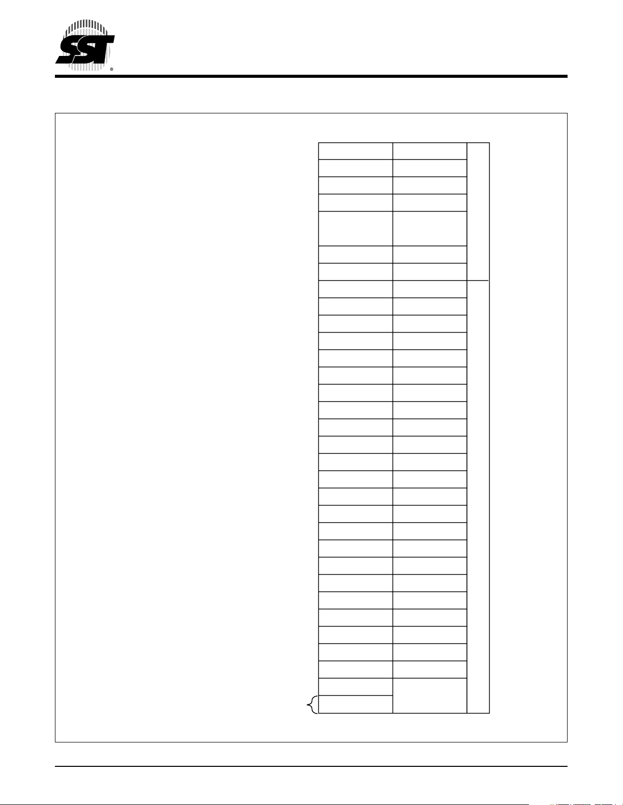
ONCURRENT READ/WRITE STATE TABLE
C
Flash
SRAMBank 1 Bank 2
Read Write No Operation
Write Read No Operation
Write No Operation Read
No Operation Write Read
Write No Operation Write
No Operation Write Write
Note: For the purposes of this table, write means to Block-, Sector,
or Chip-Erase, or Word-Program as applicable to the
appropriate bank.
Flash Read Operation
The Read operation of the SST34HF1681 is controlled by
BEF# and OE#, both have to be low for the system to
obtain data from the outputs. BEF# is used for device
selection. When BEF# is high, the chip is deselected and
only standby power is consumed. OE# is the output control
and is used to gate data from the output pins. The data bus
is in high impedance state when either BEF# or OE# is
high. Refer to the Read cycle timing diagram for further
details (Figure 6).
Flash Word-Program Operation
The SST34HF1681 are programmed on a word-by-word
basis. Before Program operations, the memory must be
erased first. The Program operation consists of three steps.
The first step is the three-byte load sequence for Software
Data Protection. The second step is to load word address
and word data. During the Word-Program operation, the
addresses are latched on the falling edge of either BEF# or
WE#, whichever occurs last. The data is latched on the rising edge of either BEF# or WE#, whichever occurs first.
The third step is the internal Program operation which is initiated after the rising edge of the fourth WE# or BEF#,
whichever occurs first. The Program operation, once initiated, will be completed typically within 10 µs. See Figures 7
and 8 for WE# and BEF# controlled Program operation timing diagrams and Figure 21 for flowcharts. During the Program operation, the only valid reads are Data# Polling and
Toggle Bit. During the internal Program operation, the host
is free to perform additional tasks. Any commands issued
during the internal Program operation are ignored.
©2001 Silicon Storage Technology, Inc. S71214-00-000 12/01 561
2
Page 3

16 Mbit Concurrent SuperFlash + 8 Mbit SRAM ComboMemory
SST34HF1681
Advance Specifications
Flash Sector/Block-Erase Operation
The Sector/Block-Erase operation allows the system to
erase the device on a sector-by-sector or block-by-block
basis. The SST34HF1681 offer both Sector-Erase and
Block-Erase mode. The sector architecture is based on
uniform sector size of 1 KWord. The Block-Erase mode is
based on uniform block size of 32 KWord. The SectorErase operation is initiated by executing a six-byte command sequence with Sector-Erase command (30H) and
sector address (SA) in the last bus cycle. The Block-Erase
operation is initiated by executing a six-byte command
sequence with Block-Erase command (50H) and block
address (BA) in the last bus cycle. The sector or block
address is latched on the falling edge of the sixth WE#
pulse, while the command (30H or 50H) is latched on the
rising edge of the sixth WE# pulse. The internal Erase
operation begins after the sixth WE# pulse. See Figures 12
and 13 for timing waveforms. Any commands issued during
the Sector- or Block-Erase operation are ignored.
Flash Chip-Erase Operation
The SST34HF1681 provide a Chip-Erase operation, which
allows the user to erase all unprotected sectors/blocks to
the “1” state. This is useful when the device must be quickly
erased.
The Chip-Erase operation is initiated by executing a sixbyte command sequence with Chip-Erase command (10H)
at address 5555H in the last byte sequence. The Erase
operation begins with the rising edge of the sixth WE# or
BEF#, whichever occurs first. During the Erase operation,
the only valid read is Toggle Bits or Data# Polling. See
Table 4 for the command sequence, Figure 11 for timing
diagram, and Figure 24 for the flowchart. Any commands
issued during the Chip-Erase operation are ignored.
Flash Write Operation Status Detection
The SST34HF1681 provide one hardware and two software means to detect the completion of a Write (Program
or Erase) cycle, in order to optimize the system Write
cycle time. The hardware detection uses the Ready/
Busy# (RY/BY#) pin. The software detection includes two
status bits: Data# Polling (DQ
The End-of-Write detection mode is enabled after the rising edge of WE#, which initiates the internal Program or
Erase operation.
The actual completion of the nonvolatile write is asynchronous with the system; therefore, either a Ready/Busy# (RY/
BY#), Data# Polling (DQ
) or Toggle Bit (DQ6) read may be
7
simultaneous with the completion of the Write cycle. If this
occurs, the system may possibly get an erroneous result,
) and Toggle Bit (DQ6).
7
i.e., valid data may appear to conflict with either DQ
. In order to prevent spurious rejection, if an erroneous
DQ
6
7
or
result occurs, the software routine should include a loop to
read the accessed location an additional two (2) times. If
both reads are valid, then the device has completed the
Write cycle, otherwise the rejection is valid.
Ready/Busy# (RY/BY#)
The SST34HF1681 includes a Ready/Busy# (RY/BY#)
output signal. During any SDP initiated operation, e.g.,
Erase, Program, CFI or ID Read operation, RY/BY# is
actively pulled low, indicating a SDP controlled operation is
in Progress. The status of RY/BY# is valid after the rising
edge of fourth WE# (or CE#) pulse for Program operation.
For Sector-, Block- or Bank-Erase, the RY/BY# is valid after
the rising edge of sixth WE# or (CE#) pulse. RY/BY# is an
open drain output that allows several devices to be tied in
parallel to V
via an external pull up resistor. Ready/
DD
Busy# is in high impedance whenever OE# or CE# is high
or RST# is low. There is a 1 µs bus recovery time (T
BR
required before valid data can be read on the data bus.
New commands can be entered immediately after RY/BY#
goes high.
Flash Data# Polling (DQ7)
When the SST34HF1681 are in the internal Program operation, any attempt to read DQ
will produce the comple-
7
ment of the true data. Once the Program operation is
completed, DQ
though DQ
will produce true data. Note that even
7
may have valid data immediately following the
7
completion of an internal Write operation, the remaining
data outputs may still be invalid: valid data on the entire
data bus will appear in subsequent successive Read
cycles. During internal Erase operation, any attempt to
read DQ
tion is completed, DQ
(DQ
will produce a ‘0’. Once the internal Erase opera-
7
will produce a ‘1’. The Data# Polling
7
) is valid after the rising edge of fourth WE# (or BEF#)
7
pulse for Program operation. For Sector-, Block- or ChipErase, the Data# Polling (DQ
) is valid after the rising edge
7
of sixth WE# (or BEF#) pulse. See Figure 9 for Data# Polling (DQ
There is a 1 µs bus recovery time (T
) timing diagram and Figure 22 for a flowchart.
7
) required before
BR
valid data can be read on the data bus. New commands
can be entered immediately after DQ
becomes true data.
7
Flash Toggle Bits (DQ6)
During the internal Program or Erase operation, any consecutive attempts to read DQ
and 0s, i.e., toggling between 1 and 0. When the internal
Program or Erase operation is completed, the DQ
stop toggling. The device is then ready for the next oper-
will produce alternating 1s
6
bit will
6
)
©2001 Silicon Storage Technology, Inc. S71214-00-000 12/01 561
3
Page 4
16 Mbit Concurrent SuperFlash + 8 Mbit SRAM ComboMemory
SST34HF1681
Advance Specifications
ation. The Toggle Bit (DQ6) is valid after the rising edge
of fourth WE# (or BEF#) pulse for Program operation.
For Sector-, Block- or Chip-Erase, the Toggle Bit (DQ
6
) is
valid after the rising edge of sixth WE# (or BEF#) pulse.
See Figure 10 for Toggle Bit timing diagram and Figure
22 for a flowchart. There is a 1 µs bus recovery time (T
BR
required before valid data can be read on the data bus.
New commands can be entered immediately after DQ
6
no
longer toggles.
Data Protection
The SST34HF1681 provide both hardware and software
features to protect nonvolatile data from inadvertent writes.
Hardware Data Protection
Noise/Glitch Protection: A WE# or BEF# pulse of less than
5 ns will not initiate a Write cycle.
Power Up/Down Detection: The Write operation is
V
DD
inhibited when V
Write Inhibit Mode:
is less than 1.5V.
DD
Forcing OE# low, BEF# high, or WE#
high will inhibit the Write operation. This prevents inadvertent writes during power-up or power-down.
Hardware Block Protection
The SST34HF1681 provide a hardware block protection
which protects the outermost 4 KWord in Bank 1. The block
is protected when WP# is held low. See Figure 1 for BlockProtection location.
A user can disable block protection by driving WP# high
thus allowing erase or program of data into the protected
sectors. WP# must be held high prior to issuing the write
command and remain stable until after the entire Write
operation has completed.
Hardware Reset (RST#)
The RST# pin provides a hardware method of resetting the
device to read array data. When the RST# pin is held low
for at least T
return to Read mode (see Figure 18). When no internal
Program/Erase operation is in progress, a minimum period
of T
RHR
Read can take place (see Figure 17).
The Erase operation that has been interrupted needs to be
reinitiated after the device resumes normal operation mode
to ensure data integrity. See Figures 17 and 18 for timing
diagrams.
any in-progress operation will terminate and
RP,
is required after RST# is driven high before a valid
Software Data Protection (SDP)
The SST34HF1681 provide the JEDEC standard Software
Data Protection scheme for all data alteration operations,
i.e., Program and Erase. Any Program operation requires
the inclusion of the three-byte sequence. The three-byte
)
load sequence is used to initiate the Program operation,
providing optimal protection from inadvertent Write operations, e.g., during the system power-up or power-down.
Any Erase operation requires the inclusion of six-byte
sequence. The SST34HF1681 are shipped with the Software Data Protection permanently enabled. See Table 4 for
the specific software command codes. During SDP command sequence, invalid commands will abort the device to
Read mode within T
. The contents of DQ15-DQ8 are
RC
“Don’t Care” during any SDP command sequence.
Common Flash Memory Interface (CFI)
The SST34HF1681 also contain the CFI information to
describe the characteristics of the device. In order to enter
the CFI Query mode, the system must write three-byte
sequence, same as Software ID Entry command with 98H
(CFI Query command) to address 555H in the last byte
sequence. Once the device enters the CFI Query mode, the
system can read CFI data at the addresses given in Tables
5 through 7. The system must write the CFI Exit command
to return to Read mode from the CFI Query mode.
Product Identification
The Product Identification mode identifies the device as the
SST34HF1681 and manufacturer as SST. This mode may
be accessed by software operations only. The hardware
device ID Read operation, which is typically used by programmers cannot be used on this device because of the
shared lines between flash and SRAM in the multi-chip
package. Therefore, application of high voltage to pin A
may damage this device. Users may use the software
Product Identification operation to identify the part (i.e.,
using the device ID) when using multiple manufacturers in
the same socket. For details, see Tables 3 and 4 for software operation, Figure 14 for the Software ID Entry and
Read timing diagram and Figure 23 for the ID Entry command sequence flowchart.
TABLE 1: P
Manufacturer’s ID 0000H 00BFH
Device ID
SST34HF1681 0001H 2761H
RODUCT IDENTIFICATION
ADDRESS DATA
9
T1.0 561
©2001 Silicon Storage Technology, Inc. S71214-00-000 12/01 561
4
Page 5
16 Mbit Concurrent SuperFlash + 8 Mbit SRAM ComboMemory
SST34HF1681
Advance Specifications
Product Identification Mode Exit/
CFI Mode Exit
In order to return to the standard Read mode, the Software
Product Identification mode must be exited. Exit is accomplished by issuing the Software ID Exit command
sequence, which returns the device to the Read mode.
This command may also be used to reset the device to the
Read mode after any inadvertent transient condition that
apparently causes the device to behave abnormally, e.g.,
not read correctly. Please note that the Software ID Exit/
CFI Exit command is ignored during an internal Program or
Erase operation. See Table 4 for software command
codes, Figure 16 for timing waveform and Figure 23 for a
flowchart.
SRAM Operation
With BES1# low, BES2 and BEF# high, the
SST34HF1681 operates as 512K x16 CMOS SRAM,
with fully static operation requiring no external clocks or
timing strobes. The SST34HF1681 SRAM is mapped
into the first 512 KWord address space. When BES1#,
BEF# are high and BES2 is low, all memory banks are
deselected and the device enters standby. Read and
Write cycle times are equal. The control signals UBS#
and LBS# provide access to the upper data byte and
lower data byte. See Table 3 for SRAM Read and Write
data byte control modes of operation.
SRAM Read
The SRAM Read operation of the SST34HF1681 is controlled by OE# and BES1#, both have to be low with WE#
and BES2 high for the system to obtain data from the outputs. BES1# and BES2 are used for SRAM bank selection.
OE# is the output control and is used to gate data from the
output pins. The data bus is in high impedance state when
OE# is high. Refer to the Read cycle timing diagram, Figure 3, for further details.
SRAM Write
The SRAM Write operation of the SST34HF1681 is controlled by WE# and BES1#, both have to be low, BES2
have to be high for the system to write to the SRAM. During
the Word-Write operation, the addresses and data are referenced to the rising edge of either BES1#, WE#, or the
falling edge of BES2 whichever occurs first. The write time
is measured from the last falling edge of BES#1 or WE# or
the rising edge of BES2 to the first rising edge of BES1#, or
WE# or the falling edge of BES2. Refer to the Write cycle
timing diagram, Figures 4 and 5, for further details.
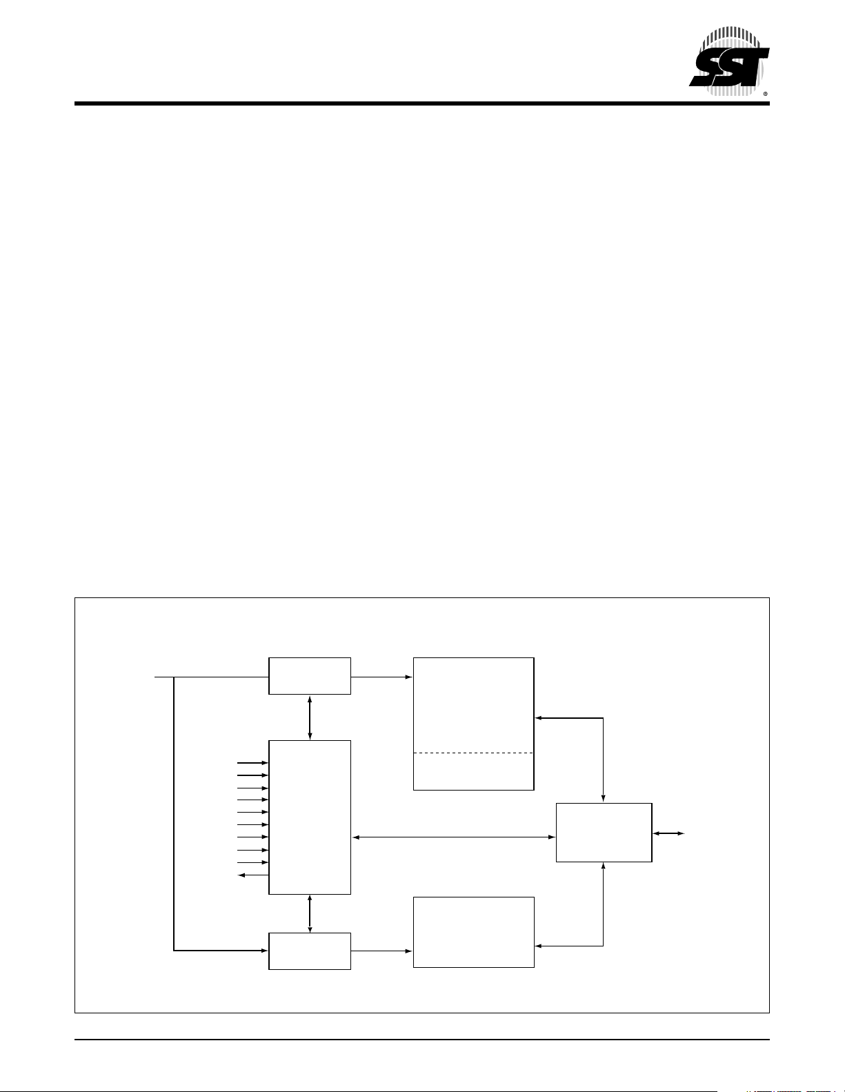
FUNCTIONAL BLOCK DIAGRAM
- A
A
MS
0
RST#
BEF#
WP#
LBS#
UBS#
WE#
OE#
BES1#
BES2
RY/BY#
AMS = Most significant address
Address
Buffers
Control
Logic
Address
Buffers
SuperFlash Memory
(Bank 1)
SuperFlash Memory
(Bank 2)
8 Mbit
SRAM
I/O Buffers
561 ILL B1.2
DQ15 - DQ
0
©2001 Silicon Storage Technology, Inc. S71214-00-000 12/01 561
5
Page 6
16 Mbit Concurrent SuperFlash + 8 Mbit SRAM ComboMemory
Bottom Sector Protection; 32 KWord Blocks; 1 KWord Sectors
SST34HF1681
Advance Specifications
4 KWord Sector Protection
(Four 1 KWord Sectors)
FFFFFH
F8000H
F7FFFH
F0000H
EFFFFH
E8000H
E7FFFH
E0000H
DFFFFH
D8000H
D7FFFH
D0000H
CFFFFH
C8000H
C7FFFH
C0000H
BFFFFH
B8000H
B7FFFH
B0000H
AFFFFH
A8000H
A7FFFH
A0000H
9FFFFH
98000H
97FFFH
90000H
8FFFFH
88000H
87FFFH
80000H
7FFFFH
78000H
77FFFH
70000H
6FFFFH
68000H
67FFFH
60000H
5FFFFH
58000H
57FFFH
50000H
4FFFFH
48000H
47FFFH
40000H
3FFFFH
38000H
37FFFH
30000H
2FFFFH
28000H
27FFFH
20000H
1FFFFH
18000H
17FFFH
10000H
00FFFFH
008000H
007FFFH
001000H
000FFFH
000000H
Block 31
Block 30
Block 29
Block 28
Block 27
Block 26
Block 25
Block 24
Block 23
Block 22
Block 21
Block 20
Block 19
Block 18
Block 17
Block 16
Block 15
Block 14
Block 13
Block 12
Block 11
Block 10
Block 9
Block 8
Block 7
Block 6
Block 5
Block 4
Block 3
Block 2
Block 1
Block 0
Bank 2
Bank 1
561 ILL F02.0
FIGURE 1: SST34HF1681, 1 MBIT X 16 CONCURRENT SUPERFLASH DUAL-BANK MEMORY ORGANIZATION
©2001 Silicon Storage Technology, Inc. S71214-00-000 12/01 561
6
Page 7
16 Mbit Concurrent SuperFlash + 8 Mbit SRAM ComboMemory
SST34HF1681
Advance Specifications
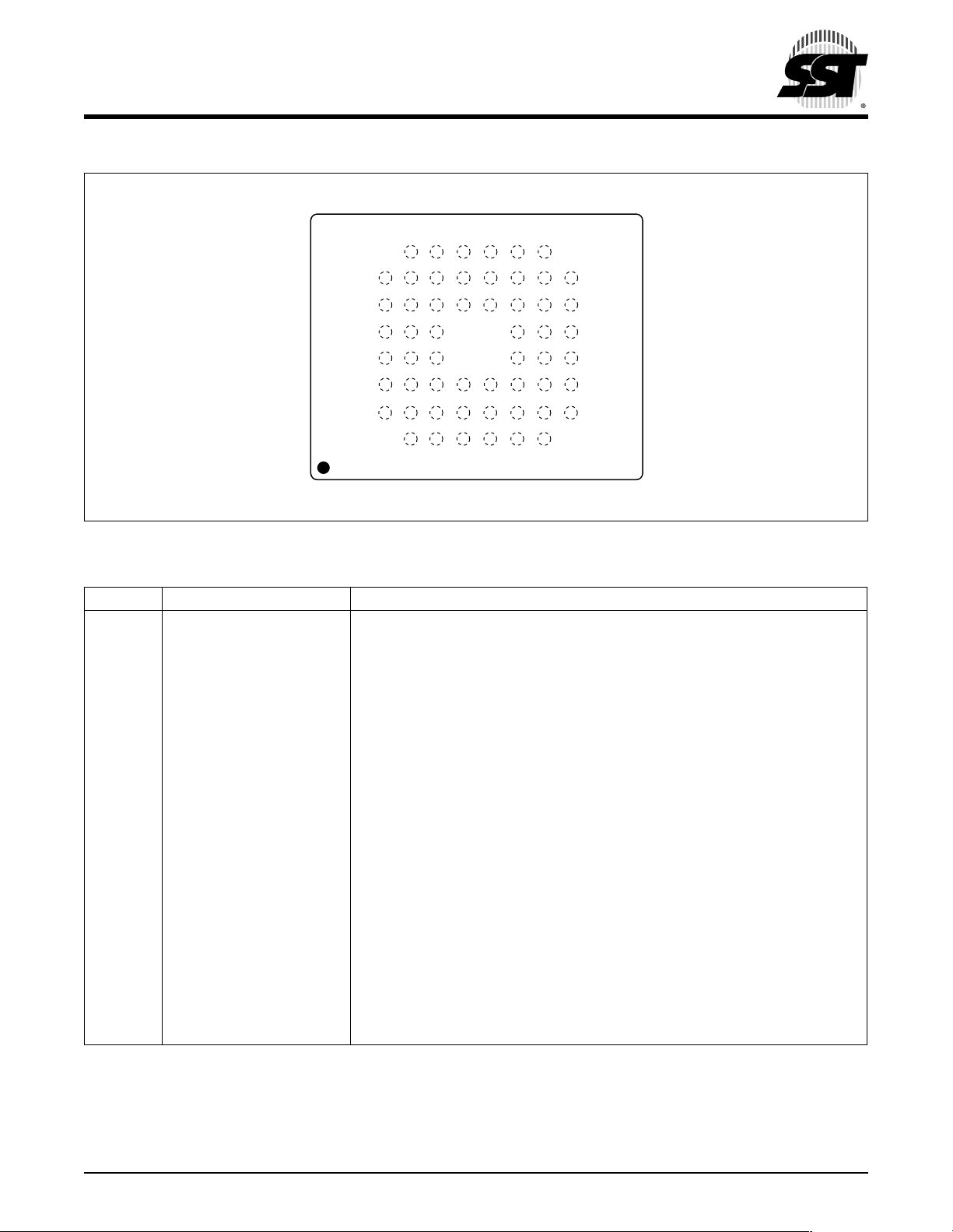
TOP VIEW (balls facing down)
8
7
6
5
4
3
2
1
A11
A8
WE#
WP#
LBS#
A7
A15
A12
A19
BES2
RST#
UBS#
A6
A3
NC
A13
A9
NC
RY/BY#
A18
A5
A2
NC
A14
A10
A17
A4
A1
A16
NC
DQ6
DQ1
V
A0
NC
V
SS
DQ7
DQ15
DQ13
DQ4
DQ3
DQ9
OE#
SS
BEF#
DQ12
V
DDS
V
DDF
DQ10
DQ0
BES1#
DQ14
DQ5
NC
DQ11
DQ2
DQ8
A B C D E F G H
SST34HF1681
561 ILL F03.0
FIGURE 2: PIN ASSIGNMENTS FOR 56-BALL LFBGA (8MM X 10MM) COMBOMEMORY PINOUT
TABLE 2: PIN DESCRIPTION
Symbol Pin Name Functions
1
A
to A
MS
DQ15-DQ0Data Inputs/Outputs To output data during Read cycles and receive input data during Write cycles.
BEF# Flash Memory Bank Enable To activate the Flash memory bank when BEF# is low
BES1# SRAM Memory Bank Enable To activate the SRAM memory bank when BES1# is low
BES2 SRAM Memory Bank Enable To activate the SRAM memory bank when BES2 is high
OE# Output Enable To gate the data output buffers
WE# Write Enable To control the Write operations
UBS# Upper Byte Control (SRAM) To enable DQ
LBS# Lower Byte Control (SRAM) To enable DQ7-DQ
WP# Write Protect To protect and unprotect sectors from Erase or Program operation
RST# Reset To Reset and return the device to Read mode
RY/BY# Ready/Busy# To output the status of a Program or Erase Operation
V
SS
V
F
DD
V
S
DD
NC No Connection Unconnected pins
1. AMS = Most Significant Address
Address Inputs To provide flash address, A19-A0.
0
To provide SRAM address, A
18-A0
Data is internally latched during a flash Erase/Program cycle. The outputs are in
tri-state when OE# is high or BES1# is high or BES2 is low and BEF# is high.
-DQ
15
8
0
RY/BY# is a open drain output, so a 10KΩ - 100KΩ pull-up resistor is required to
allow RY/BY# to transition high indicating the device is ready to read.
Ground
Power Supply (Flash) 2.7-3.3V Power Supply to Flash only
Power Supply (SRAM) 2.7-3.3V Power Supply to SRAM only
T2.1 561
©2001 Silicon Storage Technology, Inc. S71214-00-000 12/01 561
7
Page 8
16 Mbit Concurrent SuperFlash + 8 Mbit SRAM ComboMemory
TABLE 3: OPERATIONAL MODES SELECTION
Mode BEF# BES1# BES2
Full Standby V
Output Disable V
Flash Read V
Flash Write V
Flash Erase V
IH
IH
V
IL
IL
IL
IL
SRAM Read VIH VILV
SRAM Write V
Product
Identification
1. X can be VIL or VIH, but no other value.
2. Do not apply BEF# = V
3. Software mode only
4. With A
3
= 0; SST Manufacturer’s ID = 00BFH, is read with A0=0,
19-A1
IH
V
IL
, BES1# = VIL and BES2 = VIH at the same time
IL
SST34HF1681 Device ID = 2761H, is read with A
V
IH
XV
V
IL
V
IL
V
IH
XV
V
IH
XV
VIH X V
XV
VIH XVIHV
XV
V
IL
VIH X V
XV
SST34HF1681
Advance Specifications
1
2
OE# WE# LBS# UBS# DQ
0-7
X XXXXHIGH-ZHIGH-Z
IL
V
IH
V
IH
XVIHV
IL
XVILV
IL
IL
IL
IH
V
IH
IL
XXXX
V
IH
XXVIHV
IH
V
IL
XVILV
IL
V
IH
IH
IH
V
IL
IL
V
IH
V
IH
=1
0
X X HIGH-Z HIGH-Z
IH
X X HIGH-Z HIGH-Z
XXD
XX DIND
XX X X
VIL VILD
V
IH
V
IL
IL
V
IH
V
IL
V
IL
V
IH
V
IL
V
IL
V
IH
X X Manufacturer’s ID4
OUT
OUT
HIGH-Z D
D
OUT
D
IN
HIGH-Z D
D
IN
Device ID
DQ
8-15
D
OUT
IN
D
OUT
OUT
HIGH-Z
D
IN
IN
HIGH-Z
4
T3.2 561
©2001 Silicon Storage Technology, Inc. S71214-00-000 12/01 561
8
Page 9
16 Mbit Concurrent SuperFlash + 8 Mbit SRAM ComboMemory
SST34HF1681
Advance Specifications
TABLE 4: SOFTWARE COMMAND SEQUENCE
Command
Sequence
Word-Program 5555H AAH 2AAAH 55H 5555H A0H WA3Data
Sector-Erase 5555H AAH 2AAAH 55H 5555H 80H 5555H AAH 2AAAH 55H SA
Block-Erase 5555H AAH 2AAAH 55H 5555H 80H 5555H AAH 2AAAH 55H BA
Chip-Erase 5555H AAH 2AAAH 55H 5555H 80H 5555H AAH 2AAAH 55H 5555H 10H
Software ID Entry55555H AAH 2AAAH 55H 5555H 90H
CFI Query Entry
5
Software ID Exit/
CFI Exit
6
1. Address format A14-A0 (Hex),Address A
2. Data format DQ
3. WA = Program Word address
4. SA
for Sector-Erase; uses A19-A11 address lines
X
, for Block-Erase; uses A19-A15 address lines
BA
X
5. The device does not remain in Software Product Identification Mode if powered down.
6. With A
= 0; SST Manufacturer’s ID = 00BFH, is read with A0=0
20-A1
1st Bus
Write Cycle
2nd Bus
Write Cycle
3rd Bus
Write Cycle
4th Bus
Write Cycle
5th Bus
Write Cycle
6th Bus
Write Cycle
Addr1Data2Addr1Data2Addr1Data2Addr1Data2Addr1Data2Addr1Data
4
X
4
X
5555H AAH 2AAAH 55H 5555H 98H
5555H AAH 2AAAH 55H 5555H F0H
can be VIL or VIH, but no other value, for the Command sequence.
-DQ8 can be VIL or VIH, but no other value, for Command sequence.
15
SST34HF1681 Device ID = 2761H, is read with A
19-A15
=1.
0
30H
50H
T4.1 561
2
TABLE 5: CFI QUERY IDENTIFICATION STRING
1
Address Data Data
10H 0051H Query Unique ASCII string “QRY”
11H 0052H
12H 0059H
13H 0001H Primary OEM command set
14H 0007H
15H 0000H Address for Primary Extended Table
16H 0000H
17H 0000H Alternate OEM command set (00H = none exists)
18H 0000H
19H 0000H Address for Alternate OEM extended Table (00H = none exits)
1AH 0000H
1. Refer to CFI publication 100 for more details.
T5.0 561
©2001 Silicon Storage Technology, Inc. S71214-00-000 12/01 561
9
Page 10

16 Mbit Concurrent SuperFlash + 8 Mbit SRAM ComboMemory
TABLE 6: SYSTEM INTERFACE INFORMATION
Address Data Data
V
1BH 0027H
1CH 0036H VDD Max (Program/Erase)
1DH 0000H V
1EH 0000H V
1FH 0004H Typical time out for Word-Program 2
20H 0000H Typical time out for Min size buffer program 2
21H 0004H Typical time out for individual Sector/Block-Erase 2
22H 0006H Typical time out for Chip-Erase 2
23H 0001H Maximum time out for Word-Program 2
24H 0000H Maximum time out for buffer program 2
25H 0001H Maximum time out for individual Sector/Block-Erase 2
26H 0001H Maximum time out for Chip-Erase 2
Min (Program/Erase)
DD
-DQ4: Volts, DQ3-DQ0: 100 millivolts
DQ
7
DQ
-DQ4: Volts, DQ3-DQ0: 100 millivolts
7
Min (00H = no VPP pin)
PP
Max (00H = no VPP pin)
PP
1
x 24 = 32 ms)
(2
N
µs (24 = 16 µs)
N
ms (26 = 64 ms)
N
times typical (21 x 24 = 32 µs)
N
times typical
N
times typical (21 x 26 = 128 ms)
N
µs (00H = not supported)
N
ms (24 = 16 ms)
N
times typical
SST34HF1681
Advance Specifications
T6.0 561
TABLE 7: DEVICE GEOMETRY INFORMATION
Address Data Data
27H 0015H Device size = 2
28H 0001H Flash Device Interface description; 0001H = x16-only asynchronous interface
29H 0000H
2AH 0000H Maximum number of byte in multi-byte write = 2
2BH 0000H
2CH 0002H Number of Erase Sector/Block sizes supported by device
2DH 00FFH Sector Information (y + 1 = Number of sectors; z x 256B = sector size)
2EH 0003H y = 1023 + 1 = 1024 sectors (03FF = 1023)
2FH 0008H
30H 0000H z = 8 x 256 Bytes = 2 KByte/sector (0008H = 8)
31H 001FH Block Information (y + 1 = Number of blocks; z x 256B = block size)
32H 0000H y = 31 + 1 = 32 blocks (001F = 31)
33H 0000H
34H 0001H z = 256 x 256 Bytes = 64 KByte/block (0100H = 256)
N
Byte (15H = 21; 221 = 2M Bytes)
N
(00H = not supported)
T7.0 561
©2001 Silicon Storage Technology, Inc. S71214-00-000 12/01 561
10
Page 11

16 Mbit Concurrent SuperFlash + 8 Mbit SRAM ComboMemory
SST34HF1681
Advance Specifications
Absolute Maximum Stress Ratings (Applied conditions greater than those listed under “Absolute Maximum
Stress Ratings” may cause permanent damage to the device. This is a stress rating only and functional operation
of the device at these conditions or conditions greater than those defined in the operational sections of this data
sheet is not implied. Exposure to absolute maximum stress rating conditions may affect device reliability.)
Operating Temperature . . . . . . . . . . . . . . . . . . . . . . . . . . . . . . . . . . . . . . . . . . . . . . . . . . . . . . . . . . . -20°C to +85°C
Storage Temperature . . . . . . . . . . . . . . . . . . . . . . . . . . . . . . . . . . . . . . . . . . . . . . . . . . . . . . . . . . . . -65°C to +125°C
D. C. Voltage on Any Pin to Ground Potential . . . . . . . . . . . . . . . . . . . . . . . . . . . . . . . . . . . . . . .-0.5V to V
Transient Voltage (<20 ns) on Any Pin to Ground Potential . . . . . . . . . . . . . . . . . . . . . . . . . . . . . -1.0V to V
Package Power Dissipation Capability (Ta = 25°C) . . . . . . . . . . . . . . . . . . . . . . . . . . . . . . . . . . . . . . . . . . . . . . 1.0W
Output Short Circuit Current
1. VDD = V
2. Outputs shorted for no more than one second. No more than one output shorted at a time.
DDF
and V
DDS
2
. . . . . . . . . . . . . . . . . . . . . . . . . . . . . . . . . . . . . . . . . . . . . . . . . . . . . . . . . . . . . . 50 mA
OPERATING RANGE
Range Ambient Temp V
Commercial 0°C to +70°C 2.7-3.3V
Extended -20°C to +85°C 2.7-3.3V
DD
DD
DD
1
+0.3V
1
+1.0V
AC CONDITIONS OF TEST
Input Rise/Fall Time . . . . . . . . . . . . . . 5 ns
Output Load . . . . . . . . . . . . . . . . . . . . C
See Figures 19 and 20
= 30 pF
L
©2001 Silicon Storage Technology, Inc. S71214-00-000 12/01 561
11
Page 12

16 Mbit Concurrent SuperFlash + 8 Mbit SRAM ComboMemory
SST34HF1681
Advance Specifications
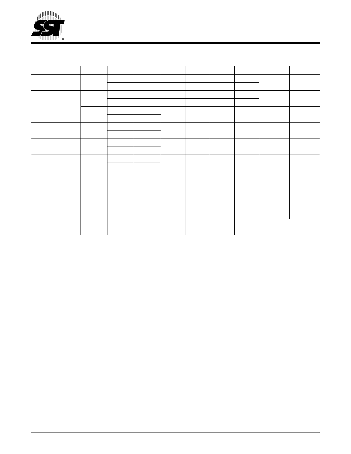
TABLE 8: DC OPERATING CHARACTERISTICS (VDD = V
Limits
Symbol Parameter
I
DD
I
SB
I
RT
I
LI
I
LO
V
IL
V
ILC
V
IH
V
IHC
V
OLF
V
OHF
V
OLS
V
OHS
1. IDD active while Erase or Program is in progress.
Active VDD Current Address input = VIL/VIH, at f=1/TRC Min,
Read OE#=V
Flash 35 mA BEF#=VIL, BES1#=VIH, or BES2=V
SRAM 30 mA BEF#=VIH, BES1#=V
Concurrent Operation 60 mA BEF#=VIH, BES1#=V
1
Write
Flash 40 mA BEF#=VIL, BES1#=VIH, or BES2=VIL, OE#=V
SRAM 30 mA BEF#=VIH, BES1#=V
Standby VDD Current 3.0V
3.3V
Reset VDD Current 30 µA Reset=VSS±0.3V
Input Leakage Current 1 µA VIN=GND to VDD, VDD=VDD Max
Output Leakage Current 1 µA V
Input Low Voltage 0.8 V VDD=VDD Min
Input Low Voltage (CMOS) 0.3 V VDD=VDD Max
Input High Voltage 0.7 V
DD
Input High Voltage (CMOS) VDD-0.3 V VDD=VDD Max
Flash Output Low Voltage 0.2 V IOL=100 µA, VDD=VDD Min
Flash Output High Voltage VDD-0.2 V IOH=-100 µA, VDD=VDD Min
SRAM Output Low Voltage 0.4 V IOL =1 mA, VDD=VDD Min
SRAM Output High Voltage 2.2 V IOH =-500 µA, VDD=VDD Min
DDF
40
75
AND V
= 2.7-3.3V)
DDS
Test ConditionsMin Max Units
V
DD=VDD
WE#=V
Max, all DQs open
, WE#=V
IL
IL
IH
IL ,
IL ,
IL ,
BES2=V
BES2=V
BES2=V
µAµAVDD = VDD Max, BEF#=BES1#=V
=GND to VDD, VDD=VDD Max
OUT
VVDD=VDD Max
IH
IH
IH
IHC,
IL
BES2=V
IH
ILC
T8.1 561
©2001 Silicon Storage Technology, Inc. S71214-00-000 12/01 561
12
Page 13

16 Mbit Concurrent SuperFlash + 8 Mbit SRAM ComboMemory
SST34HF1681
Advance Specifications
TABLE 9: RECOMMENDED SYSTEM POWER-UP TIMINGS
Symbol Parameter Minimum Units
T
T
1
PU-READ
PU-WRITE
1
1. This parameter is measured only for initial qualification and after a design or process change that could affect this parameter.
TABLE 10: CAPACITANCE (Ta = 25°C, f=1 Mhz, other pins open)
Parameter Description Test Condition Maximum
1
C
I/O
1
C
IN
1. This parameter is measured only for initial qualification and after a design or process change that could affect this parameter.
TABLE 11: FLASH RELIABILITY CHARACTERISTICS
Symbol Parameter Minimum Specification Units Test Method
1
N
END
1
T
DR
1
I
LT H
1. This parameter is measured only for initial qualification and after a design or process change that could affect this parameter.
Power-up to Read Operation 100 µs
Power-up to Write Operation 100 µs
I/O Pin Capacitance V
= 0V 20 pF
I/O
Input Capacitance VIN = 0V 16 pF
Endurance 10,000 Cycles JEDEC Standard A117
Data Retention 100 Years JEDEC Standard A103
Latch Up 100 + I
DD
mA JEDEC Standard 78
T9.0 561
T10.1 561
T11.0 561
©2001 Silicon Storage Technology, Inc. S71214-00-000 12/01 561
13
Page 14

16 Mbit Concurrent SuperFlash + 8 Mbit SRAM ComboMemory
SST34HF1681
Advance Specifications
AC CHARACTERISTICS
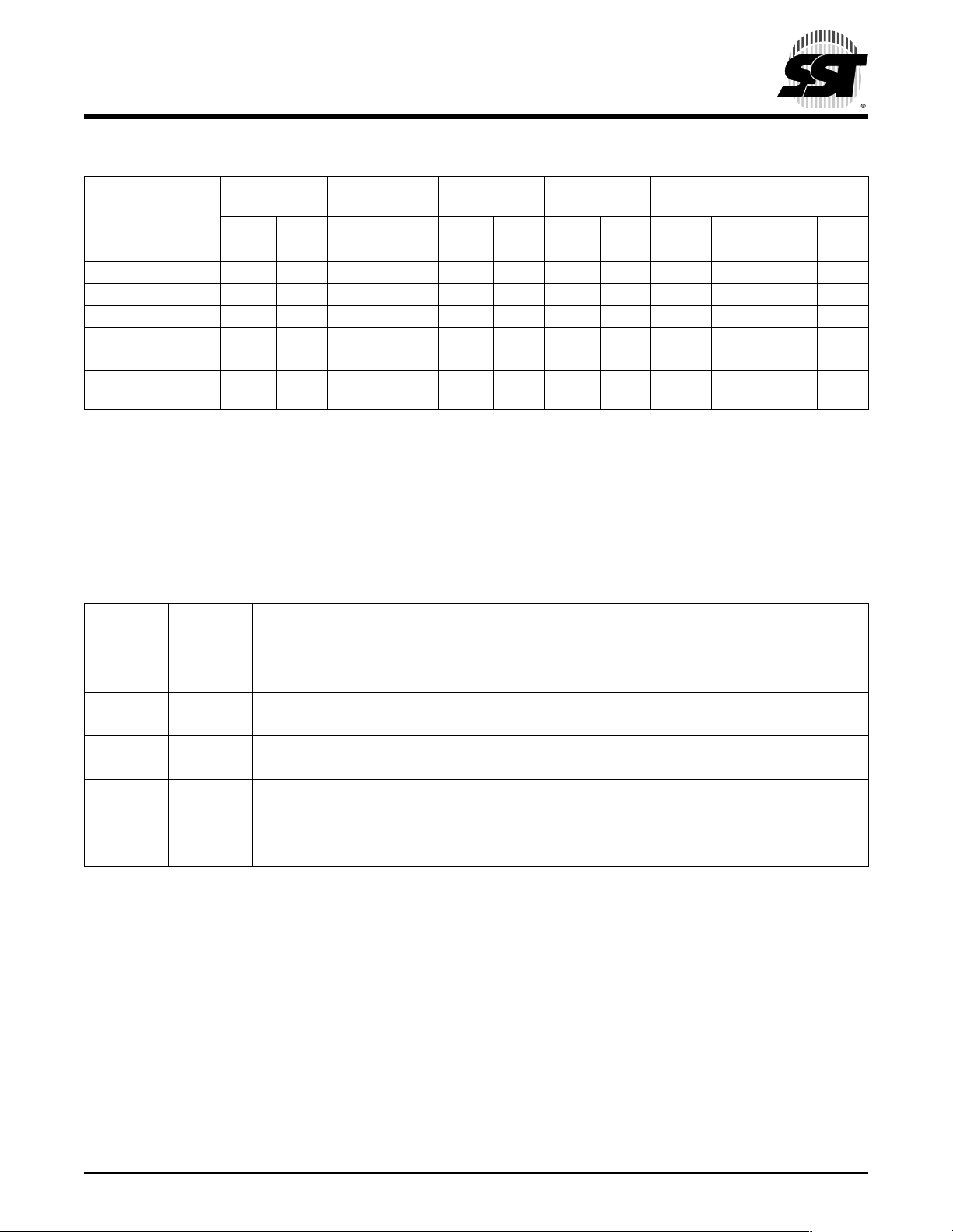
TABLE 12: SRAM READ CYCLE TIMING PARAMETERS
SST34HF1681-70 SST34HF1681-90
Symbol Parameter
T
RCS
T
AAS
T
BES
T
OES
T
BYES
1
T
BLZS
1
T
OLZS
T
BYLZS
1
T
BHZS
1
T
OHZS
T
BYHZS
T
Output Hold from Address Change 10 10 ns
OHS
1. This parameter is measured only for initial qualification and after a design or process change that could affect this parameter.
Read Cycle Time 70 90 ns
Address Access Time 70 90 ns
Bank Enable Access Time 70 90 ns
Output Enable Access Time 35 45 ns
UBS#, LBS# Access Time 70 90 ns
BES# to Active Output 0 0 ns
Output Enable to Active Output 0 0 ns
1
UBS#, LBS# to Active Output 0 0 ns
BES# to High-Z Output 25 35 ns
Output Disable to High-Z Output 25 35 ns
1
UBS#, LBS# to High-Z Output 35 45 ns
UnitsMin Max Min Max
T12.0 561
TABLE 13: SRAM WRITE CYCLE TIMING PARAMETERS
Symbol Parameter
T
WCS
T
BWS
T
AWS
T
ASTS
T
WPS
T
WRS
T
BYWS
T
ODWS
T
OEWS
T
DSS
T
DHS
Write Cycle Time 70 90 ns
Bank Enable to End-of-Write 60 80 ns
Address Valid to End-of-Write 60 80 ns
Address Set-up Time 0 0 ns
Write Pulse Width 60 80 ns
Write Recovery Time 0 0 ns
UBS#, LBS# to End-of-Write 60 80 ns
Output Disable from WE# Low 30 40 ns
Output Enable from WE# High 0 0 ns
Data Set-up Time 30 40 ns
Data Hold from Write Time 0 0 ns
SST34HF1681-70 SST34HF1681-90
UnitsMin Max Min Max
T13.0 561
©2001 Silicon Storage Technology, Inc. S71214-00-000 12/01 561
14
Page 15

16 Mbit Concurrent SuperFlash + 8 Mbit SRAM ComboMemory
SST34HF1681
Advance Specifications
TABLE 14: FLASH READ CYCLE TIMING PARAMETERS VDD = 2.7-3.3V
SST34HF1681-70 SST34HF1681-90
Symbol Parameter
T
RC
T
CE
T
AA
T
OE
1
T
CLZ
1
T
OLZ
1
T
CHZ
1
T
OHZ
1
T
OH
1
T
RP
1
T
RHR
1,2
T
RY
1. This parameter is measured only for initial qualification and after the design or process change that could affect this parameter.
2. This parameter applies to Sector-Erase, Block-Erase and Program operations. This parameter does not apply to Chip-Erase.
Read Cycle Time 70 90 ns
Chip Enable Access Time 70 90 ns
Address Access Time 70 90 ns
Output Enable Access Time 35 45 ns
BEF# Low to Active Output 0 0 ns
OE# Low to Active Output 0 0 ns
BEF# High to High-Z Output 20 30 ns
OE# High to High-Z Output 20 30 ns
Output Hold from Address Change 0 0 ns
RST# Pulse Width 500 500 ns
RST# High Before Read 50 50 ns
RST# Pin Low to Read 100 100 µs
UnitsMinMaxMinMax
T14.0 561
TABLE 15: FLASH PROGRAM/ERASE CYCLE TIMING PARAMETERS
Symbol Parameter Min Max Units
T
BP
T
AS
T
AH
T
CS
T
CH
T
OES
T
OEH
T
CP
T
WP
1
T
WPH
1
T
CPH
T
DS
1
T
DH
1
T
IDA
1
T
BY
1
T
BR
T
SE
T
BE
T
SCE
1. This parameter is measured only for initial qualification and after a design or process change that could affect this parameter.
Word-Program Time 20 µs
Address Setup Time 0 ns
Address Hold Time 40 ns
WE# and BEF# Setup Time 0 ns
WE# and BEF# Hold Time 0 ns
OE# High Setup Time 0 ns
OE# High Hold Time 10 ns
BEF# Pulse Width 40 ns
WE# Pulse Width 40 ns
WE# Pulse Width High 30 ns
BEF# Pulse Width High 30 ns
Data Setup Time 30 ns
Data Hold Time 0 ns
Software ID Access and Exit Time 150 ns
RY/BY# Delay Time 90 ns
Bus# Recovery Time 1 µs
Sector-Erase 25 ms
Block-Erase 25 ms
Chip-Erase 100 ms
T15.2 561
©2001 Silicon Storage Technology, Inc. S71214-00-000 12/01 561
15
Page 16

16 Mbit Concurrent SuperFlash + 8 Mbit SRAM ComboMemory
SST34HF1681
Advance Specifications
T
RCS
ADDRESSES A
MSS-0
BES1#
BES2
T
T
BLZS
AAS
T
BES
T
BES
OE#
T
OLZS
UBS#, LBS#
T
BYLZS
DQ
15-0
A
= Most Significant SRAM Address
MSS
FIGURE 3: SRAM READ CYCLE TIMING DIAGRAM
T
OES
T
BYES
T
WCS
DATA VALID
T
OHS
T
BHZS
T
T
BYHZS
OHZS
561 ILL F04.0
ADDRESSES A
MSS-0
T
ASTS
WE#
BES1#
BES2
UBS#, LBS#
T
ODWS
DQ
DQ
15-8,
7-0
Notes: 1. If OE# is High during the Write cycle, the outputs will remain at high impedance.
2. If BES1# goes Low or BES2 goes high coincident with or after WE# goes Low, the output will
remain at high impedance.
If BES1# goes High or BES2 goes low coincident with or before WE# goes High, the output will
remain at high impedance.
Because DIN signals may be in the output state at this time, input signals of reverse polarity
must not be applied.
NOTE 2
T
T
AWS
T
BWS
T
BWS
BYWS
T
WPS
T
DSS
VALID DATA IN
T
T
FIGURE 4: SRAM WRITE CYCLE TIMING DIAGRAM (WE# CONTROLLED)
WRS
DHS
T
OEWS
1
NOTE 2
561 ILL F05.0
©2001 Silicon Storage Technology, Inc. S71214-00-000 12/01 561
16
Page 17

16 Mbit Concurrent SuperFlash + 8 Mbit SRAM ComboMemory
SST34HF1681
Advance Specifications
T
WCS
ADDRESSES A
UBS#, LBS#
DQ
15-8,
MSS-0
T
WPS
WE#
T
BWS
BES1#
T
T
AWS
BWS
T
BYWS
T
DSS
VALID DATA IN
BES2
T
ASTS
DQ
7-0
Notes: 1. If OE# is High during the Write cycle, the outputs will remain at high impedance.
2. Because DIN signals may be in the output state at this time, input signals of reverse
polarity must not be applied.
NOTE 2
T
T
WRS
DHS
NOTE 2
561 ILL F06.0
FIGURE 5: SRAM WRITE CYCLE TIMING DIAGRAM (UBS#, LBS# CONTROLLED)
1
©2001 Silicon Storage Technology, Inc. S71214-00-000 12/01 561
17
Page 18

16 Mbit Concurrent SuperFlash + 8 Mbit SRAM ComboMemory
SST34HF1681
Advance Specifications
ADDRESS A
19-0
BEF#
OE#
T
V
IH
OLZ
WE#
T
DQ
15-0
HIGH-Z
CLZ
FIGURE 6: FLASH READ CYCLE TIMING DIAGRAM
T
RC
T
CE
T
OE
T
AA
T
OHZ
T
T
OH
CHZ
HIGH-Z
DATA VALIDDATA VALID
561 ILL F07.0
ADDRESS A
19-0
5555 2AAA 5555 ADDR
T
AH
T
WP
WE#
T
T
AS
WPH
OE#
T
BEF#
RY/BY#
DQ
15-0
T
CS
XXAA XX55 XXA0 DATA
CH
T
BY
T
DS
T
DH
WORD
(ADDR/DATA)
Note: X can be VIL or VIH, but no other value.
FIGURE 7: FLASH WE# CONTROLLED WORD-PROGRAM CYCLE TIMING DIAGRAM
T
BP
T
BR
VALID
561 ILL F08.2
©2001 Silicon Storage Technology, Inc. S71214-00-000 12/01 561
18
Page 19

16 Mbit Concurrent SuperFlash + 8 Mbit SRAM ComboMemory
SST34HF1681
Advance Specifications
T
BP
ADDRESS A
19-0
5555 2AAA 5555 ADDR
T
AH
T
CP
BEF#
T
T
AS
CPH
OE#
T
T
CH
DS
T
BY
T
DH
WE#
RY/BY#
DQ
15-0
T
CS
XXAA XX55 XXA0 DATA
WORD
(ADDR/DATA)
Note: X can be VIL or VIH, but no other value.
FIGURE 8: FLASH BEF# CONTROLLED WORD-PROGRAM CYCLE TIMING DIAGRAM
T
BR
561 ILL F09.2
VALID
ADDRESS A
19-0
T
CE
BEF#
T
T
OEH
OES
OE#
T
OE
WE#
T
BR
DQ
7
DATA# DATA# VALID DATA
561 ILL F10.1
FIGURE 9: FLASH DATA# POLLING TIMING DIAGRAM
©2001 Silicon Storage Technology, Inc. S71214-00-000 12/01 561
19
Page 20

16 Mbit Concurrent SuperFlash + 8 Mbit SRAM ComboMemory
SST34HF1681
Advance Specifications
ADDRESS A
19-0
T
CE
BEF#
T
OEH
T
OE
OE#
WE#
DQ
6
FIGURE 10: FLASH TOGGLE BIT TIMING DIAGRAM
TWO READ CYCLES
WITH SAME OUTPUTS
T
BR
VALID DATA
561 ILL F11.2
SIX-BYTE CODE FOR CHIP-ERASE
ADDRESS A
RY/BY#
DQ
19-0
BEF#
OE#
WE#
15-0
5555 2AAA 2AAA5555 5555
T
WP
Note: This device also supports BEF# controlled Chip-Erase operation. The WE# and BEF#
signals are interchageable as long as minimum timings are met. (See Table 15)
X can be V
or VIH, but no other value.
IL
5555
XX55 XX10XX55XXAA XX80 XXAA
FIGURE 11: FLASH WE# CONTROLLED CHIP-ERASE TIMING DIAGRAM
T
SCE
T
T
BY
BR
VALID
561 ILL F12.2
©2001 Silicon Storage Technology, Inc. S71214-00-000 12/01 561
20
Page 21

16 Mbit Concurrent SuperFlash + 8 Mbit SRAM ComboMemory
SST34HF1681
Advance Specifications
SIX-BYTE CODE FOR BLOCK-ERASE
ADDRESS A
RY/BY#
DQ
19-0
BEF#
OE#
WE#
15-0
5555 2AAA 2AAA5555 5555
T
WP
Note: This device also supports BEF# controlled Block-Erase operation. The WE# and BEF#
signals are interchageable as long as minimum timings are met. (See Table 15)
BA
= Block Address
X
X can be V
or VIH, but no other value.
IL
BA
X
T
BY
XX55 XX50XX55XXAA XX80 XXAA
T
BE
T
BR
VALID
561 ILL F13.2
FIGURE 12: FLASH WE# CONTROLLED BLOCK-ERASE TIMING DIAGRAM
SIX-BYTE CODE FOR SECTOR-ERASE
ADDRESS A
RY/BY#
DQ
19-0
BEF#
OE#
WE#
15-0
5555 2AAA 2AAA5555 5555
T
WP
Note: This device also supports BEF# controlled Sector-Erase operation. The WE# and BEF#
signals are interchageable as long as minimum timings are met. (See Table 15)
SA
= Sector Address
X
X can be V
or VIH, but no other value.
IL
SA
X
XX55 XX30XX55XXAA XX80 XXAA
T
SE
T
T
BY
BR
VALID
561 ILL F14.2
FIGURE 13: FLASH WE# CONTROLLED SECTOR-ERASE TIMING DIAGRAM
©2001 Silicon Storage Technology, Inc. S71214-00-000 12/01 561
21
Page 22

16 Mbit Concurrent SuperFlash + 8 Mbit SRAM ComboMemory
SST34HF1681
Advance Specifications
THREE-BYTE SEQUENCE FOR
SOFTWARE ID ENTRY
ADDRESS A
14-0
5555 2AAA 5555 0000 0001
BEF#
OE#
T
WP
WE#
T
WPH
DQ
15-0
XX55XXAA XX90
Device ID = 2761H for SST34HF1681
Note: X can be V
or VIH, but no other value
IL
FIGURE 14: FLASH SOFTWARE ID ENTRY AND READ
T
IDA
T
AA
00BF
Device ID
561 ILL F15.2
THREE-BYTE SEQUENCE FOR
CFI QUERY ENTRY
ADDRESS A
14-0
5555 2AAA 5555
BEF#
OE#
T
WP
WE#
T
WPH
DQ
15-0
Note: X can be VIL or VIH, but no other value.
XX55XXAA XX98
FIGURE 15: FLASH CFI ENTRY AND READ
T
IDA
T
AA
561 ILL F16.1
©2001 Silicon Storage Technology, Inc. S71214-00-000 12/01 561
22
Page 23

16 Mbit Concurrent SuperFlash + 8 Mbit SRAM ComboMemory
SST34HF1681
Advance Specifications
THREE-BYTE SEQUENCE FOR
SOFTWARE ID EXIT AND RESET
ADDRESS A
DQ
14-0
15-0
BEF#
OE#
WE#
5555 2AAA 5555
XXAA XX55 XXF0
T
WP
T
WHP
Note: X can be VIL or VIH, but no other value
FIGURE 16: FLASH SOFTWARE ID EXIT/CFI EXIT
RY/BY#
0V
T
RST#
RP
T
IDA
561 ILL F17.1
BEF#/OE#
T
RHR
561 ILL F26.0
FIGURE 17: RST# TIMING (WHEN NO INTERNAL OPERATION IS IN PROGRESS)
©2001 Silicon Storage Technology, Inc. S71214-00-000 12/01 561
23
Page 24

RY/BY#
RST#
16 Mbit Concurrent SuperFlash + 8 Mbit SRAM ComboMemory
SST34HF1681
Advance Specifications
T
RY
T
RP
BEF#
T
BR
OE#
FIGURE 18: RST# TIMING (DURING SECTOR- OR BLOCK-ERASE OPERATION)
V
IHT
V
V
ILT
AC test inputs are driven at V
for inputs and outputs are V
FIGURE 19: AC I
NPUT/OUTPUT REFERENCE WAVEFORMS
V
IT
(0.9 VDD) for a logic “1” and V
IHT
(0.5 VDD) and VOT (0.5 VDD). Input rise and fall times (10% ↔ 90%) are <5 ns.
IT
REFERENCE POINTS OUTPUTINPUT
(0.1 VDD) for a logic “0”. Measurement reference points
ILT
OT
561 ILL F19.1
561 ILL F20.0
Note: V
- V
- V
- V
- V
INPUT
OUTPUT
INPUT
INPUT
Tes t
Te s t
HIGH Test
LOW Test
IT
V
OT
V
IHT
V
ILT
TO TESTER
TO DUT
C
L
561 ILL F21.0
FIGURE 20: A TEST LOAD EXAMPLE
©2001 Silicon Storage Technology, Inc. S71214-00-000 12/01 561
24
Page 25

16 Mbit Concurrent SuperFlash + 8 Mbit SRAM ComboMemory
SST34HF1681
Advance Specifications
Start
Load data: XXAAH
Address: 5555H
Load data: XX55H
Address: 2AAAH
Load data: XXA0H
Address: 5555H
Note: X can be VIL or V
FIGURE 21: WORD-PROGRAM ALGORITHM
Load Word
Address/Word
Data
Wait for end of
Program (TBP,
Data# Polling
bit, or Toggle bit
operation)
Program
Completed
but no other value.
IH
,
561 ILL F22.0
©2001 Silicon Storage Technology, Inc. S71214-00-000 12/01 561
25
Page 26

16 Mbit Concurrent SuperFlash + 8 Mbit SRAM ComboMemory
SST34HF1681
Advance Specifications
Internal Timer
Program/Erase
Initiated
Wait TBP,
T
SCE, TSE
or T
BE
Program/Erase
Completed
Program/Erase
No
Toggle Bit
Initiated
Read word
Read same
word
Does DQ
6
match?
Ye s
No
Data# Polling
Program/Erase
Initiated
Read DQ
7
Is DQ7 =
true data?
Ye s
Program/Erase
Completed
FIGURE 22: WAIT OPTIONS
Program/Erase
Completed
561 ILL F23.0
©2001 Silicon Storage Technology, Inc. S71214-00-000 12/01 561
26
Page 27

16 Mbit Concurrent SuperFlash + 8 Mbit SRAM ComboMemory
SST34HF1681
Advance Specifications
CFI Query Entry
Command Sequence
Load data: XXAAH
Address: 5555H
Load data: XX55H
Address: 2AAAH
Load data: XX98H
Address: 5555H
Wait T
IDA
Read CFI data
Software Product ID Entry
Command Sequence
Load data: XXAAH
Address: 5555H
Load data: XX55H
Address: 2AAAH
Load data: XX90H
Address: 5555H
Wait T
IDA
Read Software ID
Software ID Exit/CFI Exit
Command Sequence
Load data: XXAAH
Address: 5555H
Load data: XX55H
Address: 2AAAH
Load data: XXF0H
Address: 5555H
Wait T
IDA
Return to normal
operation
561 ILL F24.1
Note: X can be VIL or V
but no other value.
IH,
FIGURE 23: SOFTWARE PRODUCT ID/CFI COMMAND FLOWCHARTS
©2001 Silicon Storage Technology, Inc. S71214-00-000 12/01 561
27
Page 28

16 Mbit Concurrent SuperFlash + 8 Mbit SRAM ComboMemory
SST34HF1681
Advance Specifications
Chip-Erase
Command Sequence
Load data: XXAAH
Address: 5555H
Load data: XX55H
Address: 2AAAH
Load data: XX80H
Address: 5555H
Load data: XXAAH
Address: 5555H
Load data: XX55H
Address: 2AAAH
Sector-Erase
Command Sequence
Load data: XXAAH
Address: 5555H
Load data: XX55H
Address: 2AAAH
Load data: XX80H
Address: 5555H
Load data: XXAAH
Address: 5555H
Load data: XX55H
Address: 2AAAH
Block-Erase
Command Sequence
Load data: XXAAH
Address: 5555H
Load data: XX55H
Address: 2AAAH
Load data: XX80H
Address: 5555H
Load data: XXAAH
Address: 5555H
Load data: XX55H
Address: 2AAAH
Load data: XX10H
Address: 5555H
Wait T
SCE
Chip erased
to FFFFH
Load data: XX30H
Address: SA
Wait T
Sector erased
to FFFFH
Note: X can be VIL or V
X
SE
but no other value.
IH,
Load data: XX50H
Address: BA
Wait T
X
BE
Block erased
to FFFFH
561 ILL F25.0
FIGURE 24: ERASE COMMAND SEQUENCE
©2001 Silicon Storage Technology, Inc. S71214-00-000 12/01 561
28
Page 29

16 Mbit Concurrent SuperFlash + 8 Mbit SRAM ComboMemory
SST34HF1681
Advance Specifications
PRODUCT ORDERING INFORMATION
Device Speed Suffix1 Suffix2
SST34
HF16xx -XXX -XX -XX
Package Modifier
P = 56 balls
Package Type
L1 = LFBGA (8mm x 10mm x 1.4mm, 0.45mm ball size)
Temperature Range
C = Commercial = 0°C to +70°C
E = Extended = -20°C to +85°C
Minimum Endurance
4 =10,000 cycles
Read Access Speed
70 = 70 ns
90 = 90 ns
Bank Split
1 = 12M + 4M
SRAM Density
0 = No SRAM
8 = 8 Mbit
Flash Density
16 = 16 Mbit
Volt age
H = 2.7-3.3V
Device Family
Valid combinations for SST34HF1681
SST34HF1681-70-4C-L1P
SST34HF1681-90-4C-L1P
SST34HF1681-70-4E-L1P
SST34HF1681-90-4E-L1P
Note: Valid combinations are those products in mass production or will be in mass production. Consult your SST sales
representative to confirm availability of valid combinations and to determine availability of new combinations.
©2001 Silicon Storage Technology, Inc. S71214-00-000 12/01 561
29
Page 30

16 Mbit Concurrent SuperFlash + 8 Mbit SRAM ComboMemory
PACKAGING DIAGRAMS
TOP VIEW
SST34HF1681
Advance Specifications
BOTTOM VIEW
10.00 ± 0.20
5.60
0.80
8
7
6
5
4
3
2
1
A1 CORNER
A B C D E F G H
SIDE VIEW
SEATING PLANE
8.00 ± 0.20
1.30 ± 0.10
0.15
0.35 ± 0.05
5.60
0.80
H G F E D C B A
Note: 1. Although many dimensions are similar to those of JEDEC Publication 95, MO-210,
this specific package is not registered.
2. All linear dimensions are in millimeters (min/max).
3. Coplanarity: 0.1 (±.05) mm.
4. The actual shape of the corners may be slightly different than as portrayed in the drawing.
56-BALL LOW-PROFILE, FINE-PITCH BALL GRID ARRAY (LFBGA) 8MM X 10MM
SST PACKAGE CODE: L1P
8
7
6
5
4
3
2
1
0.45 ± 0.05
(56X)
A1 CORNER
56ba-LFBGA-L1P-8x10-450mic-ILL.1
1mm
Silicon Storage Technology, Inc. • 1171 Sonora Court • Sunnyvale, CA 94086 • Telephone 408-735-9110 • Fax 408-735-9036
www.SuperFlash.com or www.ssti.com
©2001 Silicon Storage Technology, Inc. S71214-00-000 12/01 561
30
 Loading...