

Page 1
Technical Data Sheet SSC P485 PL Transceiver IC
Features
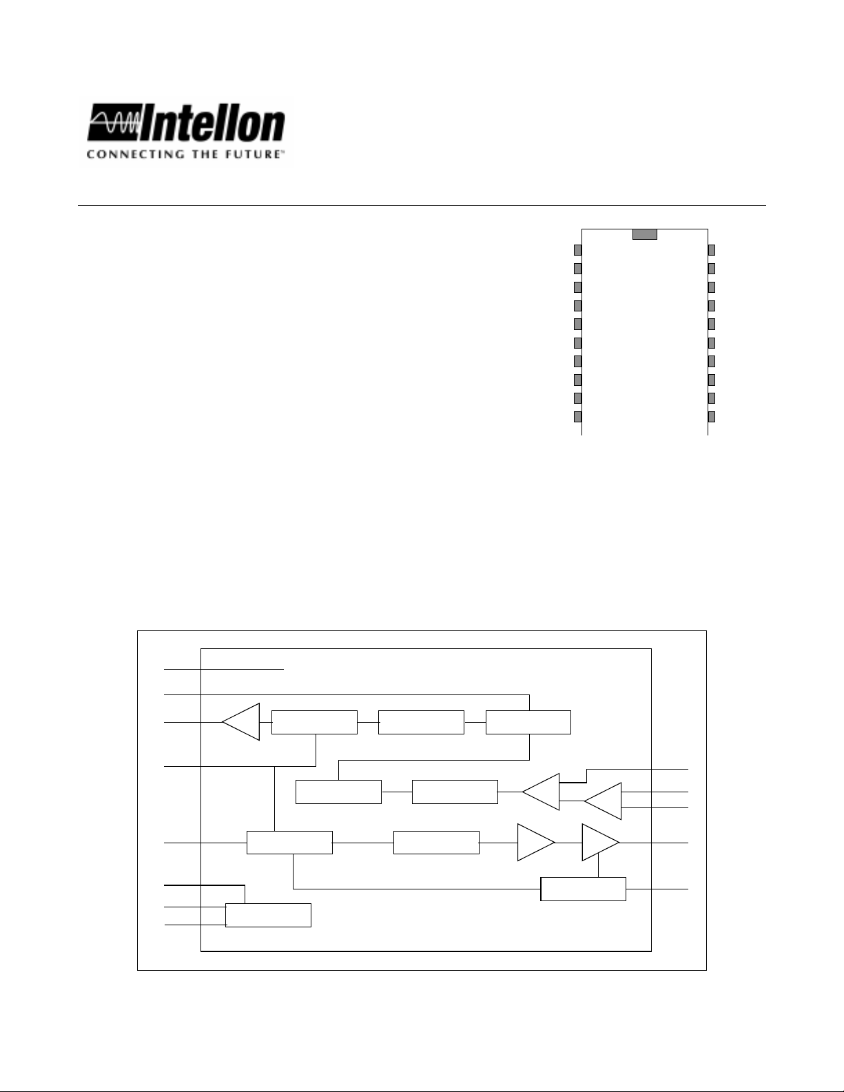
VSS
201
18
17
16
15
14
13
12
11
TP0
VDD
SI
C1
C2 VDD
SO
VSS
RST*
TS*
D
A
A
•
Enables low-cost networking products
•
Spread Spectrum Carrier communication technology
•
9600 baud data rate
•
Simple interface
•
Single +5 Volt power supply requirement
•
20 pin SOIC package
4MHZ
NC
VSS
XIN
XOUT
ILD
DI
RO
WL
219
3
D
4
5
SSC
6
D
P485
7
8
9
10
Introduction
The Intellon SSC P485 PL Transceiver IC is a highly integrated spread spectrum comm unication transceiver for
implementing low-cost networking products. The SSC P485 contains a Spread Spectrum Carrier (SSC)
transceiver, signal conditioning circuitry, and a simple host interf ace. A m inimum of exter nal circuitry is required
to connect the SSC P485 to the DC power line, twisted pair cable, or other communication medium.
The inherent reliability of SSC signaling technology provides substantial improvement in network and
communication performance over other low-cost communication methods. The SSC P485 is the ideal basic
communications element for a wide variety of low-cost networking applications.
SSC P485 Block Diagram
RST*
ILD
RO
WL
4 MHz
XIN
XOUT
RX Interface Logic
Summation
Encoder
DI
TX Interface Logic
Clock Circui t
Data Decode
Logic
Binary Shift
Register
Waveform
Generator
Tracking & Data
Extraction Logic
Comp
DAC Buf
TS Control
Amp
C2
C1
SI
SO
TS*
July 1998 Revision 5
24000828
ADVANCE INFORMATION
Page 2
SSC P485 PL Transceiver IC
Absolute Maximum Ratings (1)
Symbol Parameter Value Unit
V
DDMAX
T
V
STG
T
IN
L
DC Supply Voltage -0.3 to 7.0 V
Input Voltage at any Pin VSS-0.3 to VDD+0.3 V
Storage Temperature -65 to +150
Lead Temperature (Soldering, 10 sec onds) 300
Notes:
1. Absolute Maximum Ratings indicate limits beyond which damage to the device may occur.
Recommended Operating Conditions
Symbol Parameter Min Typical Max Unit
V
DD
F
OSC
T
A
DC Supply Voltage 4.5 5.0 5.5 V
Oscillator Frequency
Operating Temperature -40 +25 +85
Humidity (non-condensing) 95 %
12 ± 0.05%
Electrical Characteristics
Conditions: VDD = 4.5 to 5.5 V T= -40 to +85°C
°C
°C
MHz
°C
Symbol Parameter Min Typical Max Units
V
OH
V
OL
V
IH
V
IL
I
IL
v
SO
I
DD
Minimum High-level Output Voltage 2.4 V
Maximum Low-level Output Voltage (1) 0.4 V
Minimum High-level Input Voltage 2.0 V
Maximum Low-level Input Voltage 0.8 V
Maximum Input Leakage Current
SSC Signal Output Voltage (2) 4 V
Total Power Supply Current 15 mA
±10 µA
Notes:
1. TS* pin I
2. Z
= 2K Ω || 10 pF
L
= 4 mA, all other outputs IOL = 2 mA
OL
P-P
July 1998 2 Revision 5
24000828
ADVANCE INFORMATION
Page 3
SSC P485 Pin Assignments
Pin Mnemonic Name Description
1 4MHZ 4 MHz Clock Out 4 MHz clock output available for host microcontroller.
2 NC No Connect
3 VSS
D
4 XIN Crystal Input Connected to external crystal to excite the IC’s internal
5 XOUT Crystal Output Connected to external crystal to excite the IC’s internal
6VDD
D
7 ILD Idle Line Detect Digital output, active high. Logic 1 state indicates 10 bit
8 DI Driver Input Digital input. After the preamble, a low on DI (SPACE)
9 RO Receiver Output Digital output. After the preamble and assuming
10 WL Word Length Digital input. Logic 1 (default, internal pullup) selects
11 TS* Tristate Active low digital output. Enables the external output
12 RST* Reset Active low digital input. RST* asynchronously forces
13 VSS
A
14 SO Signal Output Analog signal output. Tri-state enabled with internal
15 C2 Capacitor 2 Connection for 680pF capacitor to ground.
16 C1 Capacitor 1 Connection for 680pF capacitor to ground.
17 SI Signal Input Analog signal input.
18 VDD
A
19 TP0 Test Point 0 Reserved pin for testing.
20 VSS
D
Digital Ground Digital ground reference.
Digital Supply
Analog Ground Analog ground reference.
Analog Supply
Digital Ground Digital ground reference.
SSC P485 PL Transceiver IC
oscillator and digital clock.
oscillator and digital clock.
5.0 VDC ± 10% digital supply voltage with respect to
VSS
.
D
times of idle line, logic 0 indicates detection of carrier or
non-idle line.
transmits a superior2 state on SO, a high on DI (MARK)
transmits a superior1 state on SO.
standard polarity: if superior1 state is detected on SI,
RO will be high (MARK), if superior2 state is detected
on SI, RO will be low (SPACE).
10-bit frame (START, eight data bits, STOP), logic 0
selects 11-bit frame (START, nine data bits, STOP).
amplifier when driven high. Tri-states the external
output amplifier when driven low.
RO and ILD outputs to a high state and TS* to a low
state. RST* can be asserted anytime during normal
operation to force the reset state. RST* must be active
(low) for 1 µsec after VDD
crystal oscillator stabilizes to guarantee the internal
reset state. See Figure 10.
signal.
5.0 VDC ± 10% analog supply voltage with respect to
VSS
.
A
and VDDA stabilize and the
D
July 1998 3 Revision 5
24000828
ADVANCE INFORMATION
Page 4
SSC P485 PL Transceiver IC
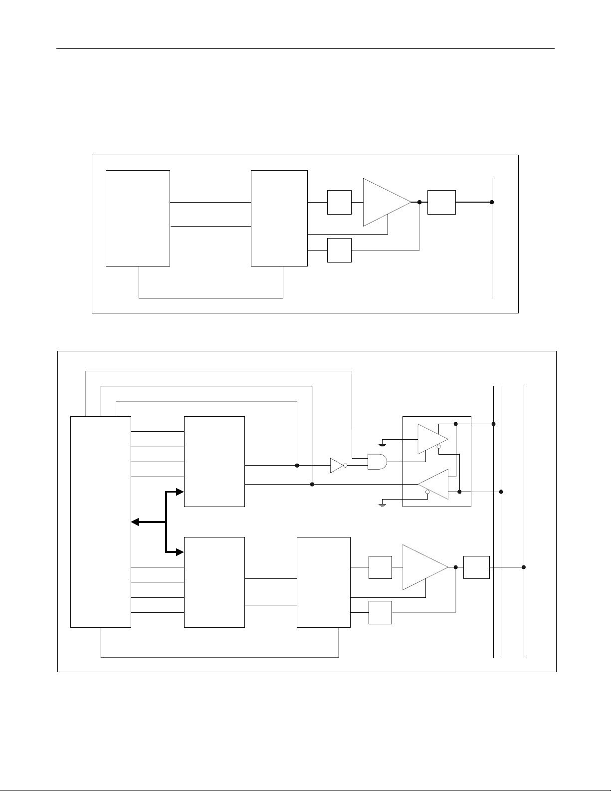
SSC P485 Application Examples
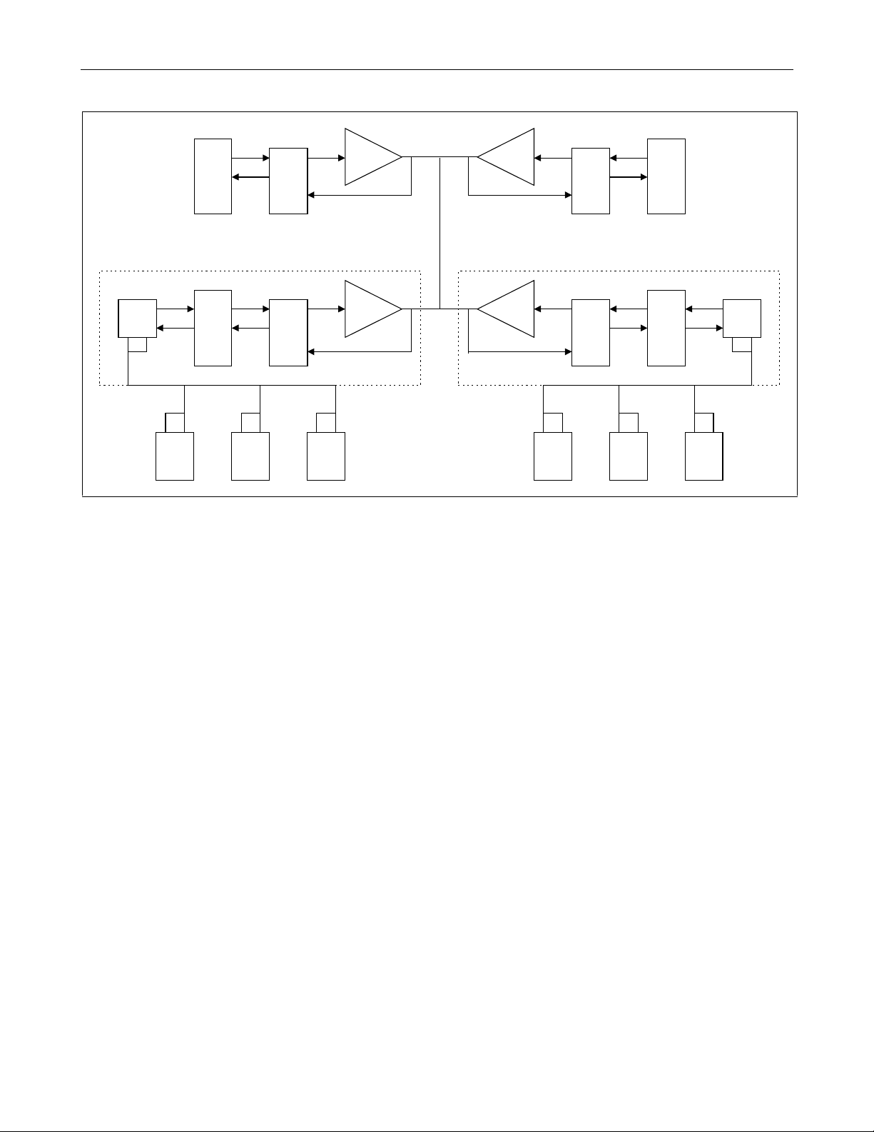
The SSC P485 may be used in a wide variety of applications. A typical node connecting to the medium is shown
in Figure 1. A gateway between an RS485 twisted pair network and a DC power line network is s hown in Figure
2. A multi-point network application with gateways using the SSC P485 is illustrated in Figure 3. Figure 4
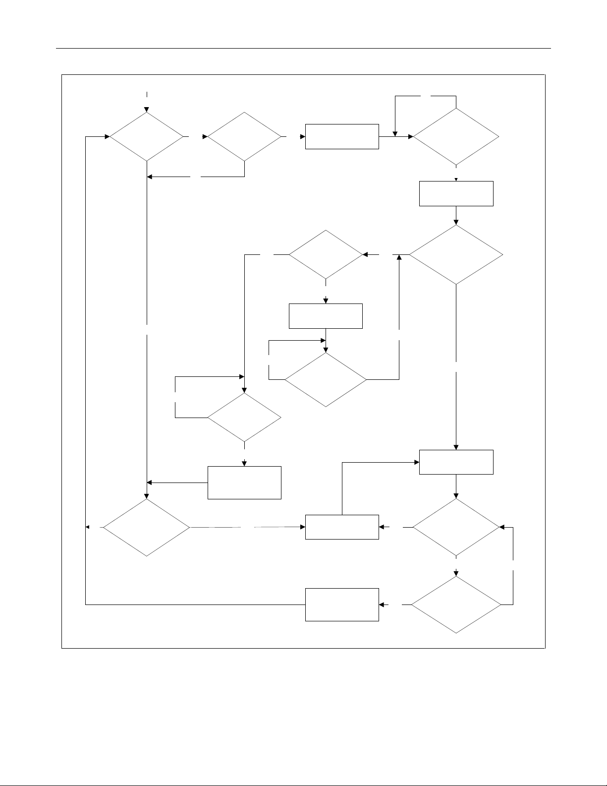
presents a host interface f low diagram showing the major steps necessary to transmit and rec eive messages
using the P485 IC.
Single
Wire
Microp rocessor
based Control
Logic
Transmit Enable #1
RXD #1
TXD #1
TXRDY #1
RXRDY #1
RD #1
WR #1
WR
RD
ILD
DI
SSC P485 PL
RO
Transceiver
SO
output
filter
SI
input
filter
Figure 1. SSC P485 Typical Node
UART
TXD #1
RXD #1
SSC P111
Power Line Media
Interface
TS*
medium
coupler
RS-485 Tra n sce iver
D
DE
R
RE*
+
-
Twisted
A
B
Pair
Single
Wire
Microprocessor
based Control
DATA 0-7
Logic
RD #2
WR #2
TXRDY #2
RXRDY #2
ILD
UART
TXD #2
RXD #2
SO
output
DI
SSC P485 PL
Transceiver
RO
SI
ILD
filter
input
filter
SSC P111
Power Line Media
Interface
TS*
medium
coupler
Figure 2. SSC P485 Gateway
July 1998 4 Revision 5
24000828
ADVANCE INFORMATION
Page 5
SSC P485 PL Transceiver IC
RS485
IC
RS485
device
P111
RS485
device
IC
P111
IC
host
micro
gate
way
micro
P485
IC
gateway gateway
P485
IC
RS485
device
DC power line
P111
P111
IC
P485
IC
IC
P485
IC
RS485
device
Figure 3. SSC P485 Multi-point Network Application
RS485
device
host
micro
gate
way
micro
RS485
IC
RS485
device
July 1998 5 Revision 5
24000828
ADVANCE INFORMATION
Page 6
SSC P485 PL Transceiver IC
Entry
message to
transmit?
No
No
No
ILD
==logic 1?Yes Yes
Yes
No
write 1st character to
UART
transmitted last
character?
No
write next character to
UART
UART indicate s
transmit buffer
available?
Yes
No
UART indicates
receive character
available?
Yes
read character from
UART
character
transmitted==character
received?
Yes
No
No
UART indicates
receive character
available?
ILD
==logic 1?
Yes
message h as been
transmitted
Yes
read character from
UART
process messag e Yes
Yes
Figure 4. Host Interface Flow Diagram
store character in
message
UART indicates
receive character
available?
No
1-1/2 char times
of quiet since last
character?
No
July 1998 6 Revision 5
24000828
ADVANCE INFORMATION
Page 7

SSC P485 PL Transceiver IC
SSC P485 Power Line Interface
Analog data is transferred between the com munication medium and the SSC P485 over the Signal In (SI) and
Signal Out (SO) pins (refer to Figur e 5). When transm itting, SSC “chir ps” f rom the SSC P485 SO pin are f iltered
by the output filter to remove harmonic energy (distortion) from the transmit signal and then amplified by the SSC
P111 Power Line Media Interface IC. The SSC P111 is a high-ef f iciency amplif ier and tri- state switch spec ific ally
designed for use in power line network systems. The amplifier is powered down and its output set to a high
impedance condition when the SSC P485 TS* signal is logic low, isolating the am plif ier f rom the rec eive c ircuitry
and reducing node power consumption during receive operation. W hen the SSC P485 TS* signal is logic high,
the communication signal is routed to the communication medium through the coupling circuit (capacitor or
transformer) . When receiving, the c ommunication signal passes through the c oupling c irc uit and is filtered by the
bandpass input filter. The res ulting signal is then applied to the SSC P485 SI pin for process ing. Refer to the
application reference shown in Figure 14.
Single
Wire
Host micro with
internal UART
ILD
TXD
RXD
DI
RO
P485
IC
Figure 5. SSC P485 Medium Coupling
SSC P485 Message Format
The P485 requires the following message formatting:
Start bits 1, logic low
Data bits 8 or 9 (default 8)
Stop bits 1, logic high
Character gap 0-4 bit times
Message gap 12 bit times minimum
Message length 1 character minimum
ILD
SO
TS*
SI
output
filter
input
filter
P111
IC
medium
coupler
July 1998 7 Revision 5
24000828
ADVANCE INFORMATION
Page 8

SSC P485 PL Transceiver IC
Transmit/Receive Timing
The SSC P485 timing with contention resolution is shown below. The P485 gener ates a pream ble based on the
first character of the m essage. Contention resolution requir es that the first charac ter of the m essage be unique
among all possible transm itters in the network . If the channel is available and the tr ansmitter wins contention, a
tracking sync sequence followed by a retransmiss ion of the first character oc curs. The P485 als o echoes the
first character back to the host allowing the host to determine that the channel was available and to continue
transmitting the message. If the channel was unavailable (the transmitter lost contention), the SO line is tristated and the first character of the received message is passed to the host. The host determines that the
channel was not available (transmitted first character does not match received first character), and the host
enters the receive message mode. Once the end of m essage is detected, the P485 drives ILD high after 10 bit
times to allow all nodes to arbitrate properly. The end of packet c ondition is true when 5 consecutive ones are
detected on DI following a stop bit. Figure 6 shows a contention resolution example for two contending
transmitters, and Figure 7 shows the end of mess age sequence and the assertion of ILD. Refer to Figure 9 f or
preamble and data encoding.
July 1998 8 Revision 5
24000828
ADVANCE INFORMATION
Page 9

SSC P485 PL Transceiver IC
Netw ork Bit Time Tracking
character 2
201
DI
SO
character 1
3407St Sp12 56
preamble character 1 character 2
S
S2 S2 S2 S2 S2
2 bit
times
sync stuff
S1 S1 S1 S1 S1 S2 S2 S1 S2 S1 S1 S2 S1 S2 S1 S1 S1
S2 S2 S2 S1 S1 S1 S2 S1 S2 S1
preamble character 1 character 2sync stuff
S S1 S1 S1 S1 S1 S2 S2 S1 S2 S1 S1 S2 S1 S2 S1 S1 S1 S2 S2 S2 S1 S1 S1 S2 S1 S2 S1
SI
character 1 echoed character 2 received
RO
3407St Sp12 56
201
ILD
Transmitter #1
character 1
DI
S S2 S2
SO
S S1 S1 S1 S1 S1 S2 S2 S1 S2 S1 S1 S2 S1 S2 S1 S1 S1 S2 S2 S2 S1 S1 S1 S2 S1 S2 S1S2 S2 S2 S2 S2
SI
RO
ILD
3407St Sp12 56
preamble
preamble character 1 character 2sync stuff
character 1 received
3407St Sp12 56
character 2 received
201 7St Sp5634 St
2 bit
times
7St Sp5634
St
01
stuff
S1 S1
S2
S1
S2
stuff
S1 S1
7St Sp5634
S2S2 S2 S2 S2 S2
S1
2.5 bit
times
S2
St
stuff
S1 S1
2.5 bit
times
S2S1 S2
Transmitter #2 (Receiver)
Figure 6. Contention Resolution Timing
July 1998 9 Revision 5
24000828
ADVANCE INFORMATION
Page 10

SSC P485 PL Transceiver IC
DI
SO
SI
RO
ILD
DI
SO
character n-1
3407St Sp12 56
character n
07St Sp12 56
34
stuff (end of msg)character n-1 character n
S1 S2 S2 S1 S2 S1 S1 S2 S1 S2 S1S1
S1 S2 S2 S1 S2 S1 S1 S2 S1 S2 S1
S1 S1 S1 S1 S1 S1
stuff (end of msg)character n-1 character n
S1 S2 S2 S1 S2 S1 S1 S2 S1 S2 S1S1 S1 S2 S2 S1 S2 S1 S1 S2 S1 S2 S1 S1 S1 S1 S1 S1 S1
character n receivedcharacter n-1 received
3407St Sp12 56
3407St Sp12 56
Transmitter
(MARK hold)
(tri-state)
10 bit times
stuff (end of msg)character n-1 character n
SI
S1 S2 S2 S1 S2 S1 S1 S2 S1 S2 S1S1 S1 S2 S2 S1 S2 S1 S1 S2 S1 S2 S1 S1 S1 S1 S1 S1 S1
character n receivedcharacter n-1 received
RO
ILD
3407St Sp12 56 3407St Sp12 56
10 bit times
Receiver
Figure 7. End of Message Timing
July 1998 10 Revision 5
24000828
ADVANCE INFORMATION
Page 11

SSC P485 PL Transceiver IC
Spread Spectrum CarrierTM Technology
Spread Spectrum CarrierTM (SSC) Technology is a method of spread spectr um communic ations suitable for both
point-to-point or carrier sens e multiple access ( CSMA) networks. Historically, spread spec trum com munication
systems have been used for secure communications and/or to overcome narrow-band impairments in the
communic ations medium. Spread spectrum r eceivers generally require an initial period of time to synchronize
with the carrier, so they have not been appropriate for CSMA networks. Spread Spectrum Carrier Technology is
a method by which a series of short, self-synchronizing, frequency swept "chirps" act as a carrier. The chirps are
always of the same known pattern and detectable by all of the nodes on the network. The chirp ranges in
frequency from 100 to 400 kHz over a duration of 100 µs. The chirp is swept from appr oximately 200 kHz to
400 kHz and then from 100 kHz to 200 kHz. Figure 8 illustrates the SSC power line chirp.
Figure 8. Spread Spectrum Carrier Chirp
Preamble Encoding
Two modulation schemes are used for s ymbol transm ission by the physical layer. Amplitude Shift Keying (ASK)
is used in the preamble of the message pac ket. ASK modulation uses SUPERIOR and INFERIOR states to
encode symbols. A SUPERIOR state is represented by the presence of a chirp and an inferior state by the
absence of a chirp. Because the trans mitter is quiet during inferior states, superior states transmitted by other
devices contending for the channel can be detected during the pream ble of the packet. An example of ASK
modulation is shown in Figure 9. Note that in the pream ble, the duration of a s ymbol is s lightly longer than in the
body of the packet. A preamble symbol is 114 µs in length. Symbols in the sync sequence and the Pac ket Body
are 100 µs in length. Please note the “Chirp” is ALW AYS 100µ s in length and is f ollowed by 14 µs of quiet tim e
during the preamble.
Data Encoding
Phase Reversal Keying (PRK) utilizes two phases of the SUPERIOR state, SUPERIOR S1 and SUPERIOR S2,
which are 180° out of phase with one another, to modulate the encoded data. This modulation technique is more
robust than the ASK technique, because it allows the P485 to correlate and track each symbol rather than just
those encoded as SUPERIOR states. Figure 9 shows an example of PRK.
July 1998 11 Revision 5
24000828
ADVANCE INFORMATION
Page 12

SSC P485 PL Transceiver IC
100 usec Phase 2 Chirp
(S2)
114 usec Superior ASK 100 usec Phase 2 Chirp
Preamble Phase
114 usec Inferior ASK
100 usec Phase 1 Chirp
(S1)
Message Body Phase
(S2: 180 degree reversal)
Figure 9. ASK and PRK Data Patterns
July 1998 12 Revision 5
24000828
ADVANCE INFORMATION
Page 13

SSC P485 PL Transceiver IC
Timing Diagrams
All timing values are referenced from the 50% mid-point between VDD and VSS. All output timings assume 50
pF load at the pin.
t
rst
RST_N
TS
ILD
RO
t
dis
t
dis
t
dis
Figure 10. Reset Timing
Table 1. Reset Timing Parameters
Symbol Parameter Min Typ Max Units Notes
t
rst
t
dis
Notes: 1. Signals are forced asynchronously to their inactive state on reset.
Reset Pulse Width 300 - - ns
Output Disable Time 3 - 20 ns 1
July 1998 13 Revision 5
24000828
ADVANCE INFORMATION
Page 14

XIN
4MHZ
t
SSC P485 PL Transceiver IC
ck12
t
d
t
pwh
t
d
t
pwl
t
ck4
Figure 11. 4 MHz Clock Output Timing
Table 2. 4 MHz Clock Timing Parameters
Symbol Parameter Min Typ Max Units Notes
t
d
t
ck12
t
ck4
t
pwh
t
pwl
Notes: 1.
Output Delay 3 - 20 ns
Input Clock Period 83.288 83.333 83.375 ns 1
Output Clock Period 249.75 250 250. 25 ns 2
Pulse Width High - 125 - ns 3
Pulse Width Low - 125 - ns 3
Oscillator frequency is 12 MHz ± 0.05%.
2.
Clock frequency is 4 MHz ± 0.1%. Assumes XIN is 12 MHz ± 0.05%.
3. Actual pulse width is determined by duty cycle of the oscillator.
July 1998 14 Revision 5
24000828
ADVANCE INFORMATION
Page 15

SSC P485 PL Transceiver IC
DI
Start
t
bit
D0 Stop
D1 D2 D3
t
byte
t
char
D7 / D8
t
bit
t
gap
Figure 12. DI Input Timing
Table 3. DI Input Timing Parameters
Symbol Parameter Min Typ Max Units Notes
t
bit
Bit Pulse Width
Baud Rate 9300 9600 9900 baud 1
t
gap
Inter-Character Gap 0 - 430.08 us
Inter-Character Bits 0 < 1 4 bits
t
byte
t
char
Byte Length 8 - 9 bits
Character Length 10 - 11 bits
Notes: 1. Corresponds to one bit width.
101.01 104.16 107.52 us 1
July 1998 15 Revision 5
24000828
ADVANCE INFORMATION
Page 16

SSC P485 PL Transceiver IC
RO
Start
t
bit
D0
t
t
byte
char
D7 / D8
StopD1 D2 D3
t
bit
t
gap
Figure 13. RO Output Timing
Table 4. RO Input Timing Parameters
Symbol Parameter Min Typ Max Units Notes
t
bit
Bit Pulse Width
Baud Rate 9576 9600 10000 baud 1
t
gap
Inter-Character Gap 0 - 469.89 us 2
Inter-Character Bits 0 - 4.5 bits 2
t
byte
t
char
Byte Length 8 - 9 bits
Character Length 10 - 11 bits
Notes: 1. Corresponds to one bit width. RO output is nominally 9600 baud. If the
received baud rate exceeds 9600 baud, the receiver will adjust RO’s output
baud rate to prevent internal buffer overflow.
2. Inter-character gap on RO’s output is a function of the received character
rate and transmitted inter-character gap. Transmitted baud rates of less
than 9600 baud increases the inter-character gap on RO’s output.
Transmitted baud rates of greater than 9600 baud decreases the intercharacter gap on RO’s output.
100.00 104.16 104.42 us 1
July 1998 16 Revision 5
24000828
ADVANCE INFORMATION
Page 17

+5V
C7 33PFC
Y1
12 MHz
C6 33PFC
HOST 4MHz
HOST ILD
HOST DI
HOST RO
HOST WL
HOST RST*
HOST INTERFACE
R12
R13
33
10
P1
P2
P3
P4
P5
P6
0.1UFZ
R4
1M
SSC P485 PL Transceiver IC
P10
P11
P7
P8
P9
60882 REV.1
HOST DC BUS
HOST GND
HOST +5V
HOST VAA
HOST GND
C5
0.1UFZ
C4
1
4MHZ
2
ILD
3
VSSD
4
XIN
5
XOUT
6
VDDD
7
NC
8
DI
9
WL
10
RO
U1 SSC_P485
10K
R5
20
VSSD
19
TP0
18
VDDA
17
SI
16
C1
15
C2
14
SO
13
VSSA
12
RST*
11
TS
C9
680PFX
C2
0.1UFZ
R9
1K
MMBT3904
PREAMP
680PFX
R3
1K
C3
220PFC
R15
24K
Q2
Q3
MMBT3904
R14
47
C8
VAA
R6
10K
R2
13K
D1
ADK
BAV99
C16
3300PFX
C18
1500PFX
R10
1.2K
BUFFER
Q1
MMBT3904
180UH
R11
C13
100
3300PFX
TRANSMIT PREFILTER
L3
180UH
C17
3300PFX
INPUT FILTER
L2
C12
1500PFX
C15
.01UFX
L4
120UH
C11
0.1UFZ
R1
510
1N5819
VAA
R8
OUTPUT FILTER / TRANSIENT PROTECTION
180
VAA
VAA
D2
CEXT
BIAS
NC
VSS
NC
NC
VDD
TXI
D5
P6KE10A
D4
P6KE10A
16
15
14
13
12
11
10
9
1.0UF, 63V
75K, 1%
D3
1N5819
1
2
3
4
5
6
7
8
L1
1.8UH NLC
VSS
VDD
VSS
TXO
VSS
VDD
TP0
TS
U2 SSC_P111
C19
22UF,25V
C14
0.1UFZ
C10
C1
1.0UFX
R7
LINE COUPLING
TX1
1 2
1.0UF, 63V
3 4
12:12
+5V
C21
22UF,25V
C22
D6
P6KE24C
DC BUS INTERFACE
VAA
C20
33UF,25V
POWER SUPPLY
Figure 14. P485 Reference Application
July 1998 17 Revision 5
24000828
ADVANCE INFORMATION
Page 18

SSC P485 PL Transceiver IC
SSC P485 Mechanical Specifications
Dimensions in Inches
Figure 15. 20-Pin SOIC Package Outline
July 1998 18 Revision 5
24000828
ADVANCE INFORMATION
Page 19

Ordering Information
SSC P485 PL Transceiver IC
SSC P485 PL Transceiver IC
5100 West Silver Springs Boulevard
Ocala, Florida 34482
Phone: (352) 237-7416
Fax: (352) 237-7616
Internet
http://www.intellon.com
ftp://ftp.intellon.com
Intellon Corporation, 1998. Intellon Corporation reserves the right t o make changes to this data sheet without notice. Intellon Corporation
makes no warranty, representation or guarantee regarding the suitability of its products for any part icular purpose. Intellon Corporation
assumes no liability arising out of the applic ation or use of any product or circuit. Intellon Corporat ion specifically disclaims any and all
liability, including without limitation consequent ial or incidental damages.
July 1998 19 Revision 5
24000828
ADVANCE INFORMATION
 Loading...