

Page 1

13.56 MHz short-range contactless memory chip
– Unsawn wafer
– Bumped and sawn wafer
with 4096-bit EEPROM and anticollision functions
Features
■ ISO 14443-2 Type B air interface compliant
■ ISO 14443-3 Type B frame format compliant
■ 13.56 MHz carrier frequency
■ 847 kHz subcarrier frequency
■ 106 Kbit/second data transfer
■ 8 bit Chip_ID based anticollision system
■ 2 count-down binary counters with automated
antitearing protection
■ 64-bit Unique Identifier
■ 4096-bit EEPROM with write protect feature
■ Read_block and Write_block (32 bits)
■ Internal tuning capacitor
■ 1million erase/write cycles
■ 40-year data retention
■ Self-timed programming cycle
■ 5 ms typical programming time
SRI4K
September 2011 Doc 11605 Rev 5 1/46
www.st.com
1
Page 2

Contents SRI4K
Contents
1 Description . . . . . . . . . . . . . . . . . . . . . . . . . . . . . . . . . . . . . . . . . . . . . . . . . 7
2 Signal description . . . . . . . . . . . . . . . . . . . . . . . . . . . . . . . . . . . . . . . . . . . 8
2.1 AC1, AC0 . . . . . . . . . . . . . . . . . . . . . . . . . . . . . . . . . . . . . . . . . . . . . . . . . . 8
3 Data transfer . . . . . . . . . . . . . . . . . . . . . . . . . . . . . . . . . . . . . . . . . . . . . . . 9
3.1 Input data transfer from the reader to the SRI4K (request frame) . . . . . . . 9
3.1.1 Character transmission format for request frame . . . . . . . . . . . . . . . . . . 9
3.1.2 Request start of frame . . . . . . . . . . . . . . . . . . . . . . . . . . . . . . . . . . . . . . 10
3.1.3 Request end of frame . . . . . . . . . . . . . . . . . . . . . . . . . . . . . . . . . . . . . . 10
3.2 Output data transfer from the SRI4K to the reader (answer frame) . . . . . 11
3.2.1 Character transmission format for answer frame . . . . . . . . . . . . . . . . . . 11
3.2.2 Answer start of frame . . . . . . . . . . . . . . . . . . . . . . . . . . . . . . . . . . . . . . . 11
3.2.3 Answer end of frame . . . . . . . . . . . . . . . . . . . . . . . . . . . . . . . . . . . . . . . 12
3.3 Transmission frame . . . . . . . . . . . . . . . . . . . . . . . . . . . . . . . . . . . . . . . . . 12
3.4 CRC . . . . . . . . . . . . . . . . . . . . . . . . . . . . . . . . . . . . . . . . . . . . . . . . . . . . . 13
4 Memory mapping . . . . . . . . . . . . . . . . . . . . . . . . . . . . . . . . . . . . . . . . . . 14
4.1 Resettable OTP area . . . . . . . . . . . . . . . . . . . . . . . . . . . . . . . . . . . . . . . . 15
4.2 32-bit binary counters . . . . . . . . . . . . . . . . . . . . . . . . . . . . . . . . . . . . . . . . 16
4.3 EEPROM area . . . . . . . . . . . . . . . . . . . . . . . . . . . . . . . . . . . . . . . . . . . . . 17
4.4 System area . . . . . . . . . . . . . . . . . . . . . . . . . . . . . . . . . . . . . . . . . . . . . . . 17
4.4.1 OTP_Lock_Reg . . . . . . . . . . . . . . . . . . . . . . . . . . . . . . . . . . . . . . . . . . . 18
4.4.2 Fixed Chip_ID (Option) . . . . . . . . . . . . . . . . . . . . . . . . . . . . . . . . . . . . . 18
5 SRI4K operation . . . . . . . . . . . . . . . . . . . . . . . . . . . . . . . . . . . . . . . . . . . 19
6 SRI4K states . . . . . . . . . . . . . . . . . . . . . . . . . . . . . . . . . . . . . . . . . . . . . . 20
6.1 Power-off state . . . . . . . . . . . . . . . . . . . . . . . . . . . . . . . . . . . . . . . . . . . . . 20
6.2 Ready state . . . . . . . . . . . . . . . . . . . . . . . . . . . . . . . . . . . . . . . . . . . . . . . 20
6.3 Inventory state . . . . . . . . . . . . . . . . . . . . . . . . . . . . . . . . . . . . . . . . . . . . . 20
6.4 Selected state . . . . . . . . . . . . . . . . . . . . . . . . . . . . . . . . . . . . . . . . . . . . . 20
6.5 Deselected state . . . . . . . . . . . . . . . . . . . . . . . . . . . . . . . . . . . . . . . . . . . . 20
2/46 Doc 11605 Rev 5
Page 3

SRI4K Contents
6.6 Deactivated state . . . . . . . . . . . . . . . . . . . . . . . . . . . . . . . . . . . . . . . . . . . 20
7 Anticollision . . . . . . . . . . . . . . . . . . . . . . . . . . . . . . . . . . . . . . . . . . . . . . . 22
7.1 Description of an anticollision sequence . . . . . . . . . . . . . . . . . . . . . . . . . 24
8 SRI4K commands . . . . . . . . . . . . . . . . . . . . . . . . . . . . . . . . . . . . . . . . . . 27
8.1 Initiate() command . . . . . . . . . . . . . . . . . . . . . . . . . . . . . . . . . . . . . . . . . . 28
8.2 Pcall16() command . . . . . . . . . . . . . . . . . . . . . . . . . . . . . . . . . . . . . . . . . 29
8.3 Slot_marker(SN) command . . . . . . . . . . . . . . . . . . . . . . . . . . . . . . . . . . . 30
8.4 Select(Chip_ID) command . . . . . . . . . . . . . . . . . . . . . . . . . . . . . . . . . . . . 31
8.5 Completion() command . . . . . . . . . . . . . . . . . . . . . . . . . . . . . . . . . . . . . . 32
8.6 Reset_to_inventory() command . . . . . . . . . . . . . . . . . . . . . . . . . . . . . . . . 33
8.7 Read_block(Addr) command . . . . . . . . . . . . . . . . . . . . . . . . . . . . . . . . . . 34
8.8 Write_block (Addr, Data) command . . . . . . . . . . . . . . . . . . . . . . . . . . . . . 35
8.9 Get_UID() command . . . . . . . . . . . . . . . . . . . . . . . . . . . . . . . . . . . . . . . . 36
8.10 Power-on state . . . . . . . . . . . . . . . . . . . . . . . . . . . . . . . . . . . . . . . . . . . . . 37
9 Maximum rating . . . . . . . . . . . . . . . . . . . . . . . . . . . . . . . . . . . . . . . . . . . . 38
10 DC and ac parameters . . . . . . . . . . . . . . . . . . . . . . . . . . . . . . . . . . . . . . 39
11 Part numbering . . . . . . . . . . . . . . . . . . . . . . . . . . . . . . . . . . . . . . . . . . . . 41
Appendix A ISO-14443 Type B CRC calculation . . . . . . . . . . . . . . . . . . . . . . . . . 42
Appendix B SRI4K command summary . . . . . . . . . . . . . . . . . . . . . . . . . . . . . . . . 43
Revision history . . . . . . . . . . . . . . . . . . . . . . . . . . . . . . . . . . . . . . . . . . . . . . . . . . . . 45
Doc 11605 Rev 5 3/46
Page 4

List of tables SRI4K
List of tables
Table 1. Signal names . . . . . . . . . . . . . . . . . . . . . . . . . . . . . . . . . . . . . . . . . . . . . . . . . . . . . . . . . . . . 7
Table 2. Bit description . . . . . . . . . . . . . . . . . . . . . . . . . . . . . . . . . . . . . . . . . . . . . . . . . . . . . . . . . . . 10
Table 3. SRI4K memory mapping. . . . . . . . . . . . . . . . . . . . . . . . . . . . . . . . . . . . . . . . . . . . . . . . . . . 14
Table 4. Standard anticollision sequence . . . . . . . . . . . . . . . . . . . . . . . . . . . . . . . . . . . . . . . . . . . . . 24
Table 5. Command code . . . . . . . . . . . . . . . . . . . . . . . . . . . . . . . . . . . . . . . . . . . . . . . . . . . . . . . . . 27
Table 6. Absolute maximum ratings . . . . . . . . . . . . . . . . . . . . . . . . . . . . . . . . . . . . . . . . . . . . . . . . . 38
Table 7. Operating conditions. . . . . . . . . . . . . . . . . . . . . . . . . . . . . . . . . . . . . . . . . . . . . . . . . . . . . . 39
Table 8. DC characteristics. . . . . . . . . . . . . . . . . . . . . . . . . . . . . . . . . . . . . . . . . . . . . . . . . . . . . . . . 39
Table 9. AC characteristics. . . . . . . . . . . . . . . . . . . . . . . . . . . . . . . . . . . . . . . . . . . . . . . . . . . . . . . . 39
Table 10. Ordering information scheme . . . . . . . . . . . . . . . . . . . . . . . . . . . . . . . . . . . . . . . . . . . . . . . 41
Table 11. Document revision history . . . . . . . . . . . . . . . . . . . . . . . . . . . . . . . . . . . . . . . . . . . . . . . . . 45
4/46 Doc 11605 Rev 5
Page 5

SRI4K List of figures
List of figures
Figure 1. Logic diagram . . . . . . . . . . . . . . . . . . . . . . . . . . . . . . . . . . . . . . . . . . . . . . . . . . . . . . . . . . . . 7
Figure 2. Die floor plan. . . . . . . . . . . . . . . . . . . . . . . . . . . . . . . . . . . . . . . . . . . . . . . . . . . . . . . . . . . . . 8
Figure 3. 10% ASK modulation of the received wave . . . . . . . . . . . . . . . . . . . . . . . . . . . . . . . . . . . . . 9
Figure 4. SRI4K request frame character format . . . . . . . . . . . . . . . . . . . . . . . . . . . . . . . . . . . . . . . . . 9
Figure 5. Request start of frame . . . . . . . . . . . . . . . . . . . . . . . . . . . . . . . . . . . . . . . . . . . . . . . . . . . . 10
Figure 6. Request end of frame . . . . . . . . . . . . . . . . . . . . . . . . . . . . . . . . . . . . . . . . . . . . . . . . . . . . . 10
Figure 7. Wave transmitted using BPSK subcarrier modulation . . . . . . . . . . . . . . . . . . . . . . . . . . . . 11
Figure 8. Answer start of frame . . . . . . . . . . . . . . . . . . . . . . . . . . . . . . . . . . . . . . . . . . . . . . . . . . . . . 11
Figure 9. Answer end of frame. . . . . . . . . . . . . . . . . . . . . . . . . . . . . . . . . . . . . . . . . . . . . . . . . . . . . . 12
Figure 10. Example of a complete transmission frame . . . . . . . . . . . . . . . . . . . . . . . . . . . . . . . . . . . . 12
Figure 11. CRC transmission rules . . . . . . . . . . . . . . . . . . . . . . . . . . . . . . . . . . . . . . . . . . . . . . . . . . . 13
Figure 12. Resettable OTP area (addresses 0 to 4) . . . . . . . . . . . . . . . . . . . . . . . . . . . . . . . . . . . . . . 15
Figure 13. Write_block update in Standard mode (binary format) . . . . . . . . . . . . . . . . . . . . . . . . . . . . 15
Figure 14. Write_block update in Reload mode (binary format). . . . . . . . . . . . . . . . . . . . . . . . . . . . . . 15
Figure 15. Binary counter (addresses 5 to 6). . . . . . . . . . . . . . . . . . . . . . . . . . . . . . . . . . . . . . . . . . . . 16
Figure 16. Countdown example (binary format). . . . . . . . . . . . . . . . . . . . . . . . . . . . . . . . . . . . . . . . . . 16
Figure 17. EEPROM (addresses 7 to 127) . . . . . . . . . . . . . . . . . . . . . . . . . . . . . . . . . . . . . . . . . . . . . 17
Figure 18. System area . . . . . . . . . . . . . . . . . . . . . . . . . . . . . . . . . . . . . . . . . . . . . . . . . . . . . . . . . . . . 18
Figure 19. State transition diagram . . . . . . . . . . . . . . . . . . . . . . . . . . . . . . . . . . . . . . . . . . . . . . . . . . . 21
Figure 20. SRI4K Chip_ID description . . . . . . . . . . . . . . . . . . . . . . . . . . . . . . . . . . . . . . . . . . . . . . . . . 22
Figure 21. Description of a possible anticollision sequence . . . . . . . . . . . . . . . . . . . . . . . . . . . . . . . . 23
Figure 22. Example of an anticollision sequence. . . . . . . . . . . . . . . . . . . . . . . . . . . . . . . . . . . . . . . . . 26
Figure 23. Initiate request format . . . . . . . . . . . . . . . . . . . . . . . . . . . . . . . . . . . . . . . . . . . . . . . . . . . . . 28
Figure 24. Initiate response format . . . . . . . . . . . . . . . . . . . . . . . . . . . . . . . . . . . . . . . . . . . . . . . . . . . 28
Figure 25. Initiate frame exchange between reader and SRI4K . . . . . . . . . . . . . . . . . . . . . . . . . . . . . 28
Figure 26. Pcall16 request format . . . . . . . . . . . . . . . . . . . . . . . . . . . . . . . . . . . . . . . . . . . . . . . . . . . . 29
Figure 27. Pcall16 response format . . . . . . . . . . . . . . . . . . . . . . . . . . . . . . . . . . . . . . . . . . . . . . . . . . . 29
Figure 28. Pcall16 frame exchange between reader and SRI4K . . . . . . . . . . . . . . . . . . . . . . . . . . . . . 29
Figure 29. Slot_marker request format . . . . . . . . . . . . . . . . . . . . . . . . . . . . . . . . . . . . . . . . . . . . . . . . 30
Figure 30. Slot_marker response format . . . . . . . . . . . . . . . . . . . . . . . . . . . . . . . . . . . . . . . . . . . . . . . 30
Figure 31. Slot_marker frame exchange between reader and SRI4K . . . . . . . . . . . . . . . . . . . . . . . . . 30
Figure 32. Select request format . . . . . . . . . . . . . . . . . . . . . . . . . . . . . . . . . . . . . . . . . . . . . . . . . . . . . 31
Figure 33. Select response format . . . . . . . . . . . . . . . . . . . . . . . . . . . . . . . . . . . . . . . . . . . . . . . . . . . . 31
Figure 34. Select frame exchange between reader and SRI4K. . . . . . . . . . . . . . . . . . . . . . . . . . . . . . 31
Figure 35. Completion request format . . . . . . . . . . . . . . . . . . . . . . . . . . . . . . . . . . . . . . . . . . . . . . . . . 32
Figure 36. Completion response format. . . . . . . . . . . . . . . . . . . . . . . . . . . . . . . . . . . . . . . . . . . . . . . . 32
Figure 37. Completion frame exchange between reader and SRI4K . . . . . . . . . . . . . . . . . . . . . . . . . 32
Figure 38. Reset_to_inventory request format. . . . . . . . . . . . . . . . . . . . . . . . . . . . . . . . . . . . . . . . . . . 33
Figure 39. Reset_to_inventory response format . . . . . . . . . . . . . . . . . . . . . . . . . . . . . . . . . . . . . . . . . 33
Figure 40. Reset_to_inventory frame exchange between reader and SRI4K . . . . . . . . . . . . . . . . . . . 33
Figure 41. Read_block request format. . . . . . . . . . . . . . . . . . . . . . . . . . . . . . . . . . . . . . . . . . . . . . . . . 34
Figure 42. Read_block response format . . . . . . . . . . . . . . . . . . . . . . . . . . . . . . . . . . . . . . . . . . . . . . . 34
Figure 43. Read_block frame exchange between reader and SRI4K . . . . . . . . . . . . . . . . . . . . . . . . . 34
Figure 44. Write_block request format . . . . . . . . . . . . . . . . . . . . . . . . . . . . . . . . . . . . . . . . . . . . . . . . . 35
Figure 45. Write_block response format . . . . . . . . . . . . . . . . . . . . . . . . . . . . . . . . . . . . . . . . . . . . . . . 35
Figure 46. Write_block frame exchange between reader and SRI4K . . . . . . . . . . . . . . . . . . . . . . . . . 36
Figure 47. Get_UID request format . . . . . . . . . . . . . . . . . . . . . . . . . . . . . . . . . . . . . . . . . . . . . . . . . . . 36
Figure 48. Get_UID response format . . . . . . . . . . . . . . . . . . . . . . . . . . . . . . . . . . . . . . . . . . . . . . . . . . 36
Doc 11605 Rev 5 5/46
Page 6

List of figures SRI4K
Figure 49. 64-bit unique identifier of the SRI4K . . . . . . . . . . . . . . . . . . . . . . . . . . . . . . . . . . . . . . . . . . 37
Figure 50. Get_UID frame exchange between reader and SRI4K. . . . . . . . . . . . . . . . . . . . . . . . . . . . 37
Figure 51. SRI4K synchronous timing, transmit and receive . . . . . . . . . . . . . . . . . . . . . . . . . . . . . . . . 40
Figure 52. Initiate frame exchange between reader and SRI4K . . . . . . . . . . . . . . . . . . . . . . . . . . . . . 43
Figure 53. Pcall16 frame exchange between reader and SRI4K . . . . . . . . . . . . . . . . . . . . . . . . . . . . . 43
Figure 54. Slot_marker frame exchange between reader and SRI4K . . . . . . . . . . . . . . . . . . . . . . . . . 43
Figure 55. Select frame exchange between reader and SRI4K. . . . . . . . . . . . . . . . . . . . . . . . . . . . . . 43
Figure 56. Completion frame exchange between reader and SRI4K . . . . . . . . . . . . . . . . . . . . . . . . . 43
Figure 57. Reset_to_inventory frame exchange between reader and SRI4K . . . . . . . . . . . . . . . . . . . 44
Figure 58. Read_block frame exchange between reader and SRI4K . . . . . . . . . . . . . . . . . . . . . . . . . 44
Figure 59. Write_block frame exchange between reader and SRI4K . . . . . . . . . . . . . . . . . . . . . . . . . 44
Figure 60. Get_UID frame exchange between reader and SRI4K. . . . . . . . . . . . . . . . . . . . . . . . . . . . 44
6/46 Doc 11605 Rev 5
Page 7
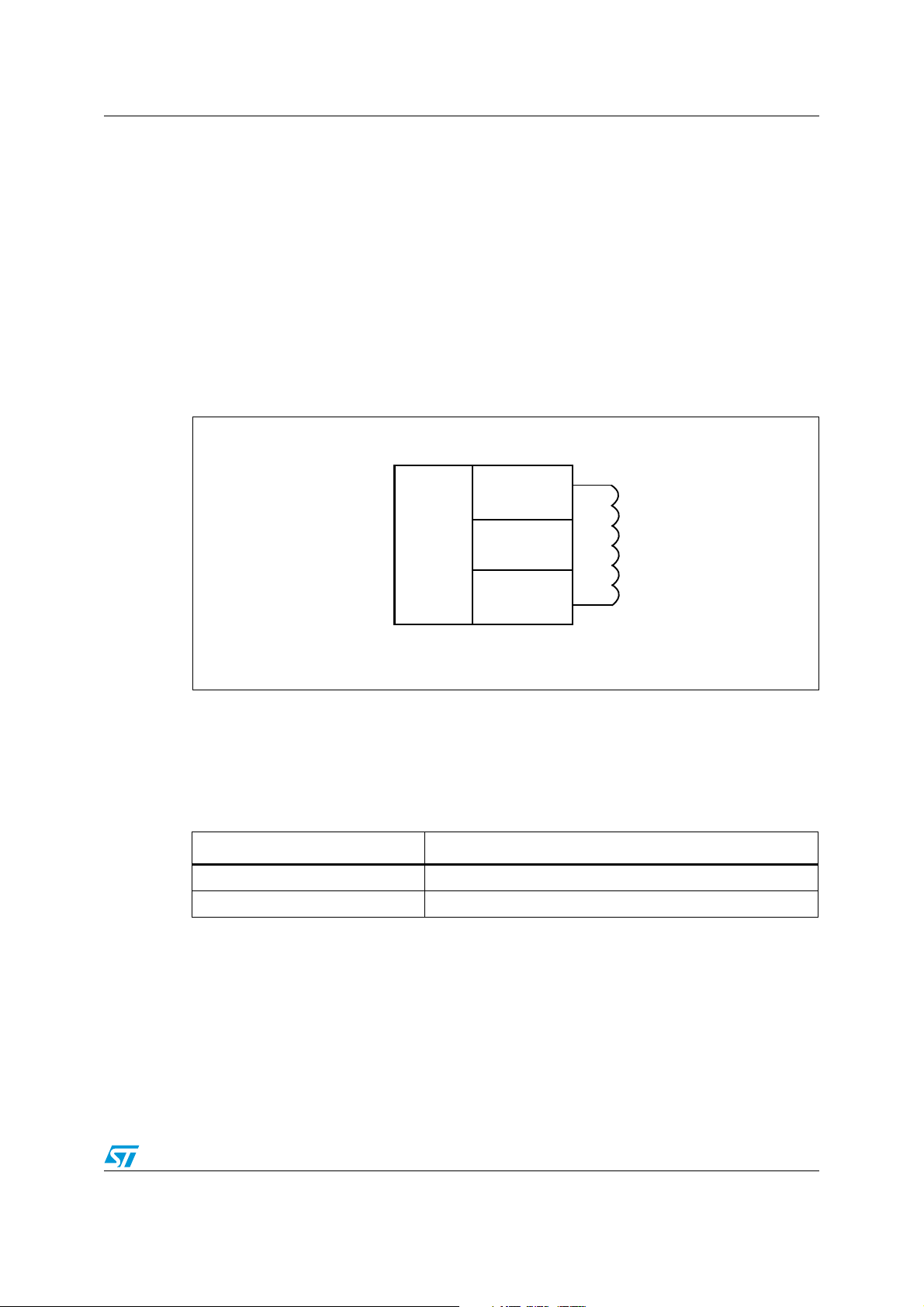
SRI4K Description
AI10878
AC1
SRI4K
AC0
Power
Supply
Regulator
BPSK
Load
Modulator
ASK
Demodulator
4 Kbit
User
EEPROM
1 Description
The SRI4K is a contactless memory, powered by an externally transmitted radio wave. It
contains a 4096-bit user EEPROM. The memory is organized as 128 blocks of 32 bits. The
SRI4K is accessed via the 13.56 MHz carrier. Incoming data are demodulated and decoded
from the received amplitude shift keying (ASK) modulation signal and outgoing data are
generated by load variation using bit phase shift keying (BPSK) coding of a 847 kHz
subcarrier. The received ASK wave is 10% modulated. The data transfer rate between the
SRI4K and the reader is 106 kbit/s in both reception and emission modes.
The SRI4K follows the ISO 14443 part 2 type B recommendation for the radio-frequency
power and signal interface.
Figure 1. Logic diagram
The SRI4K is specifically designed for short range applications that need re-usable
products. The SRI4K includes an anticollision mechanism that allows it to detect and select
tags present at the same time within range of the reader. The anticollision is based on a
probabilistic scanning method using slot markers. Using the STMicroelectronics single chip
coupler, CRX14, it is easy to design a reader and build a contactless system.
Table 1. Signal names
Signal names Description
AC1 Antenna coil
AC0 Antenna coil
Doc 11605 Rev 5 7/46
Page 8

Signal description SRI4K
AI09055
AC1AC0
The SRI4K contactless EEPROM can be randomly read and written in block mode (each
block containing 32 bits). The instruction set includes the following nine commands:
● Read_block
● Write_block
● Initiate
● Pcall16
● Slot_marker
● Select
● Completion
● Reset_to_inventory
● Get_UID
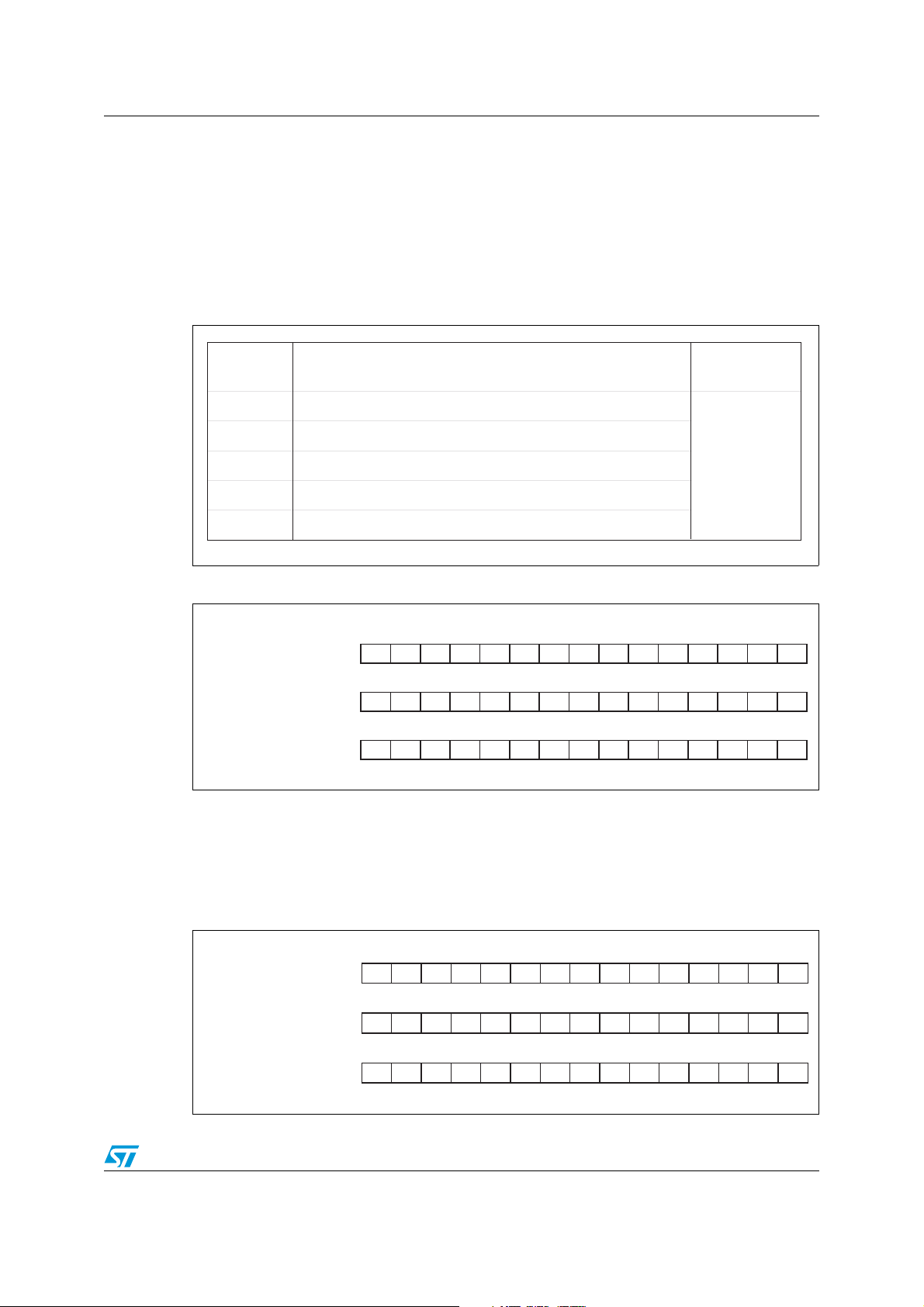
The SRI4K memory is organized in three areas, as described in Figure 3. The first area is a
resettable OTP (one time programmable) area in which bits can only be switched from 1 to
0. Using a special command, it is possible to erase all bits of this area to 1. The second area
provides two 32-bit binary counters which can only be decremented from FFFF FFFFh to
0000 0000h, and gives a capacity of 4,294,967,296 units per counter. The last area is the
EEPROM memory. It is accessible by block of 32 bits and includes an auto-erase cycle
during each Write_block command.
Figure 2. Die floor plan
2 Signal description
2.1 AC1, AC0
The pads for the Antenna Coil. AC1 and AC0 must be directly bonded to the antenna.
8/46 Doc 11605 Rev 5
Page 9

SRI4K Data transfer
DATA BIT TO TRANSMIT
TO THE
10% ASK MODULATION
OF THE 13.56MHz WAVE,
GENERATED BY THE READER
Transfer time for one data bit is 1/106 kHz
SRI4K
AI10880
ai07664
1 ETU
Start
"0"
Stop
"1"
MSbLSb Information Byte
b0 b1 b2 b3 b4 b5 b6 b7 b8 b9
3 Data transfer
3.1 Input data transfer from the reader to the SRI4K (request frame)
The reader must generate a 13.56 MHz sinusoidal carrier frequency at its antenna, with
enough energy to “remote-power” the memory. The energy received at the SRI4K’s antenna
is transformed into a supply voltage by a regulator, and into data bits by the ASK
demodulator. For the SRI4K to decode correctly the information it receives, the reader must
10% amplitude-modulate the 13.56 MHz wave before sending it to the SRI4K. This is
represented in Figure 3. The data transfer rate is 106 Kbits/s.
Figure 3. 10% ASK modulation of the received wave
3.1.1 Character transmission format for request frame
The SRI4K transmits and receives data bytes as 10-bit characters, with the least significant
bit (b
) transmitted first, as shown in Figure 4. Each bit duration, an ETU (elementary time
0
unit), is equal to 9.44 µs (1/106 kHz).
These characters, framed by a start of frame (SOF) and an end of frame (EOF), are put
together to form a command frame as shown in Figure 10. A frame includes an SOF,
commands, addresses, data, a CRC and an EOF as defined in the ISO 14443-3 Type B
Standard. If an error is detected during data transfer, the SRI4K does not execute the
command, but it does not generate an error frame.
Figure 4. SRI4K request frame character format
Doc 11605 Rev 5 9/46
Page 10
Data transfer SRI4K
ai07665
ETU
b0 b1 b2 b3 b4 b5 b6 b7 b8 b9 b10 b11
000000000011
ai07666
ETU
b0 b1 b2 b3 b4 b5 b6 b7 b8 b9
0000000000
Table 2. Bit description
Bit Description Value
b
0
b1 to b
b
9
Start bit used to synchronize the transmission b0 = 0
Information byte (command, address or data)
8
Stop bit used to indicate the end of a character b9 = 1
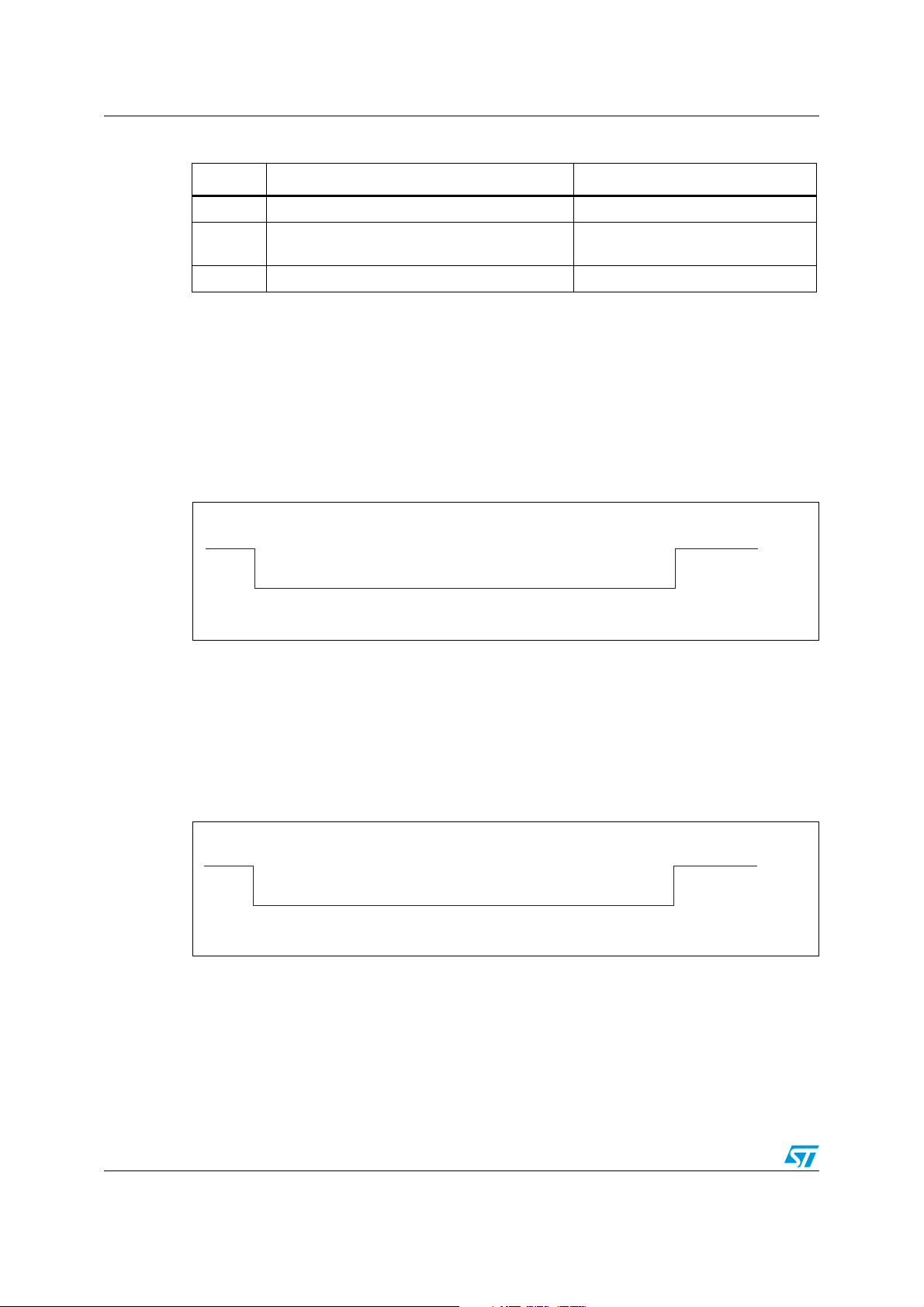
3.1.2 Request start of frame
The SOF described in Figure 5 is composed of:
● one falling edge,
● followed by 10 ETUs at logic-0,
● followed by a single rising edge,
● followed by at least 2 ETUs (and at most 3) at logic-1.
Figure 5. Request start of frame
The information byte is sent with the
least significant bit first
3.1.3 Request end of frame
The EOF shown in Figure 6 is composed of:
● one falling edge,
● followed by 10 ETUs at logic-0,
● followed by a single rising edge.
Figure 6. Request end of frame
10/46 Doc 11605 Rev 5
Page 11

SRI4K Data transfer
Or
AI10881
Data Bit to be Transmitted
to the Reader
847kHz BPSK Modulation
Generated by the SRI4K
BPSK Modulation at 847kHz
During a One-bit Data Transfer Time (1/106kHz)
ai07665
ETU
b0 b1 b2 b3 b4 b5 b6 b7 b8 b9 b10 b11
000000000011
3.2 Output data transfer from the SRI4K to the reader (answer frame)
The data bits issued by the SRI4K use retro-modulation. Retro-modulation is obtained by
modifying the SRI4K current consumption at the antenna (load modulation). The load
modulation causes a variation at the reader antenna by inductive coupling. With appropriate
detector circuitry, the reader is able to pick up information from the SRI4K. To improve loadmodulation detection, data is transmitted using a BPSK encoded, 847 kHz subcarrier
frequency ƒ
Figure 7. Wave transmitted using BPSK subcarrier modulation
as shown in Figure 7, and as specified in the ISO 14443-2 Type B Standard.
s
3.2.1 Character transmission format for answer frame
3.2.2 Answer start of frame
The character format is the same as for input data transfer (Figure 4). The transmitted
frames are made up of an SOF, data, a CRC and an EOF (Figure 10). As with an input data
transfer, if an error occurs, the reader does not issue an error code to the SRI4K, but it
should be able to detect it and manage the situation. The data transfer rate is
106 Kbits/second.
The SOF described in Figure 8 is composed of:
● followed by 10 ETUs at logic-0
● followed by 2 ETUs at logic-1
Figure 8. Answer start of frame
Doc 11605 Rev 5 11/46
Page 12

Data transfer SRI4K
ai07665
ETU
b0 b1 b2 b3 b4 b5 b6 b7 b8 b9 b10 b11
000000000011
12 bits
10 bits
Sync
128/fs
128/fs
fs=847.5kHz
t
DR
t
0
t
1
SOF
Cmd
Data CRC CRC
EOF
10 bits 10 bits 10 bits 10 bits
12 bits
10 bits 10 bits 10 bits
Data CRC CRC
SOF
EOF
12 bits
SOF
t
2
AI10882
Input data transfer using ASK Output data transfer using BPSK
Sent by the
Reader
Sent by the
SRI4K
at 106kb/s
3.2.3 Answer end of frame
The EOF shown in Figure 9 is composed of:
● followed by 10 ETUs at logic-0,
● followed by 2 ETUs at logic-1.
Figure 9. Answer end of frame
3.3 Transmission frame
Between the request data transfer and the answer data transfer, all ASK and BPSK
modulations are suspended for a minimum time of t
to switch from Transmission to Reception mode. It is repeated after each frame. After t
13.5 6MHz carrier frequency is modulated by the SRI4K at 847 kHz for a period of t
128/ƒ
to allow the reader to synchronize. After t1, the first phase transition generated by the
S
SRI4K forms the start bit (‘0’) of the answer SOF. After the falling edge of the answer EOF,
the reader waits a minimum time, t
, before sending a new request frame to the SRI4K.
2
= 128/ƒS. This delay allows the reader
0
, the
0
=
1
Figure 10. Example of a complete transmission frame
12/46 Doc 11605 Rev 5
Page 13

SRI4K Data transfer
CRC 16 (8 bits) CRC 16 (8 bits)
LSbit MSbit LSbit MSbit
LSByte MSByte
ai07667
3.4 CRC
The 16-bit CRC used by the SRI4K is generated in compliance with the ISO14443 Type B
recommendation. For further information, please see Appendix A. The initial register
contents are all 1s: FFFFh.
The two-byte CRC is present in every request and in every answer frame, before the EOF.
The CRC is calculated on all the bytes between SOF (not included) and the CRC field.
Upon reception of a request from a reader, the SRI4K verifies that the CRC value is valid. If
it is invalid, the SRI4K discards the frame and does not answer the reader.
Upon reception of an answer from the SRI4K, the reader should verify the validity of the
CRC. In case of error, the actions to be taken are the reader designer’s responsibility.
The CRC is transmitted with the least significant byte first and each byte is transmitted with
the least significant bit first.
Figure 11. CRC transmission rules
Doc 11605 Rev 5 13/46
Page 14

Memory mapping SRI4K
4 Memory mapping
The SRI4K is organized as 128 blocks of 32 bits as shown in Tabl e 3 . All blocks are
accessible by the Read_block command. Depending on the write access, they can be
updated by the Write_block command. A Write_block updates all the 32 bits of the block.
Table 3. SRI4K memory mapping
Block
Addr
MSB 32-bit block LSB
b
31
b
24 b23
b16 b
15
b8 b
7
b
0 32 bits Boolean area
1 32 bits Boolean area
2 32 bits Boolean area
3 32 bits Boolean area
4 32 bits Boolean area
5 32 bits binary counter
6 32 bits binary counter
7User area
8User area
9User area
10 User area
11 User area
12 User area
13 User area
14 User area
15 User area
16 User area
Description
0
Resettable OTP
bits
Count down
counter
Lockable
EEPROM
127 User area
255 OTP_Lock_Reg ST Reserved
UID0
64 bits UID area ROM
UID1
14/46 Doc 11605 Rev 5
Fixed Chip_ID
(Option)
EEPROM... User area
System OTP
bits
Page 15
SRI4K Memory mapping
Block
address
MSb
b31
32-bit block
b16 b15b24 b23 b8 b7
LSb
b0
Description
Resettable
OTP bit
0
1
2
3
4
32-bit Boolean area
32-bit Boolean area
32-bit Boolean area
32-bit Boolean area
32-bit Boolean area
ai07657b
ai07658
1 ... 1 1 01011111 0 11
1 ... 1 0 01011001 1 11
1 ... 1 0 01011001 0 11
Previous data stored in block
Data to be written
New data stored in block
b31 b0
ai07659
1...110 1011111 0 11
1...111 1011001 1 11
1 ... 1 1 1 1011001 1 11
Previous data stored in block
Data to be written
New data stored in block
b31 b0
4.1 Resettable OTP area
In this area contains five individual 32-bit Boolean words (see Figure 12 for a map of the
area). A Write_block command will not erase the previous contents of the block as the write
cycle is not preceded by an auto-erase cycle. This feature can be used to reset selected bits
from 1 to 0. All bits previously at 0 remain unchanged. When the 32 bits of a block are all at
0, the block is empty, and cannot be updated any more. See Figure 13 and Figure 14 for
examples of the result of the Write_block command in the resettable OTP area.
Figure 12. Resettable OTP area (addresses 0 to 4)
Figure 13. Write_block update in Standard mode (binary format)
The five 32-bit blocks making up the resettable OTP area can be erased in one go by adding
an auto-erase cycle to the Write_block command. An auto-erase cycle is added each time
the SRI4K detects a Reload command. The Reload command is implemented through a
specific update of the 32-bit binary counter located at block address 6 (see “Section 4.2: 32-
bit binary counters” for details).
Figure 14. Write_block update in Reload mode (binary format)
Doc 11605 Rev 5 15/46
Page 16
Memory mapping SRI4K
Block
Address
MSb
b31
32-bit block
b16 b15b24 b23 b8 b7
LSb
b0
Description
Count down
Counter
5
6
32-bit binary counter
32-bit binary counter
ai07660b
ai07661
1...1111111111111
1...1111111111110
1...1111111111101
Initial data
1-unit decrement
1-unit decrement
b31 b0
1...1111111111100
1...1111111110100
1...1111111111000
1-unit decrement
8-unit decrement
Increment not allowed
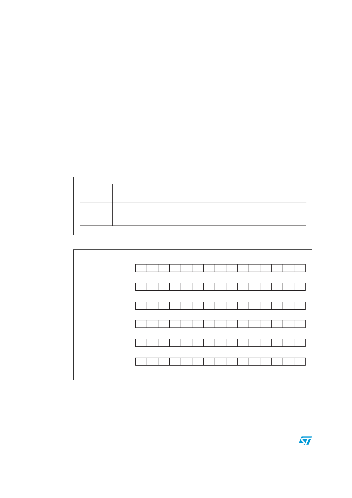
4.2 32-bit binary counters
The two 32-bit binary counters located at block addresses 5 and 6, respectively, are used to
count down from 2
32
(4096 million) to 0. The SRI4K uses dedicated logic that only allows
the update of a counter if the new value is lower than the previous one. This feature allows
the application to count down by steps of 1 or more. The initial value in Counter 5 is
FFFF FFFEh and is FFFF FFFFh in Counter 6. When the value displayed is 0000 0000h,
the counter is empty and cannot be reloaded. The counter is updated by issuing the
Write_block command to block address 5 or 6, depending on which counter is to be
updated. The Write_block command writes the new 32-bit value to the counter block
address. Figure 16 shows examples of how the counters operate.
The counter programming cycles are protected by automated antitearing logic. This function
allows the counter value to be protected in case of power down within the programming
cycle. In case of power down, the counter value is not updated and the previous value
continues to be stored.
Figure 15. Binary counter (addresses 5 to 6)
Figure 16. Countdown example (binary format)
The counter with block address 6 controls the Reload command used to reset the resettable
OTP area (addresses 0 to 4). Bits b
of these 11 bits is updated, the SRI4K detects the change and adds an Erase cycle to the
Write_block command for locations 0 to 4 (see the “Resettable OTP area” paragraph). The
Erase cycle remains active until a Power-off or a Select command is issued. The SRI4K’s
resettable OTP area can be reloaded up to 2 047 times (2
to b21 act as an 11-bit Reload counter; whenever one
31
11
-1).
16/46 Doc 11605 Rev 5
Page 17

SRI4K Memory mapping
Block
address
MSb
b31
32-bit block
b16 b15b24 b23 b8 b7
LSb
b0
Description
Lockable
EEPROM
7
8
9
10
11
User area
User area
User area
User area
User area
Ai07662c
13
14
15
16
...
User area
User area
User area
User area
User area
12
127
User area
User area
EEPROM
4.3 EEPROM area
The 121 blocks between addresses 7 and 127 are EEPROM blocks of 32 bits each (484
bytes in total). (See Figure 17 for a map of the area.) These blocks can be accessed using
the Read_block and Write_block commands. The Write_block command for the EEPROM
area always includes an auto-erase cycle prior to the write cycle.
Blocks 7 to 15 can be write-protected. Write access is controlled by the 8 bits of the
OTP_Lock_Reg located at block address 255 (see “OTP_Lock_Reg” for details). Once
protected, these blocks (7 to 15) cannot be unprotected.
Figure 17. EEPROM (addresses 7 to 127)
4.4 System area
This area is used to modify the settings of the SRI4K. It contains 3 registers:
OTP_Lock_Reg, Fixed Chip_ID and ST Reserved. See Figure 18 for a map of this area.
A Write_block command in this area will not erase the previous contents. Selected bits can
thus be set from 1 to 0. All bits previously at 0 remain unchanged. Once all the 32 bits of a
block are at 0, the block is empty and cannot be updated any more.
Doc 11605 Rev 5 17/46
Page 18

Memory mapping SRI4K
Block
address
255
MSb
b31 b24 b23
32-bit block
b16 b15 b8 b7 b0
LSb
Description
OTP
OTP_Lock_Reg ST reserved
Fixed Chip_ID
(Option)
ai07663b
Figure 18. System area
4.4.1 OTP_Lock_Reg
The 8 bits, b31 to b24, of the System area (block address 255) are used as OTP_Lock_Reg
bits in the SRI4K. They control the write access to the 9 EEPROM blocks with addresses 7
to 15 as follows:
● When b
● When b
● When b
● When b
● When b
● When b
● When b
● When b
The OTP_Lock_Reg bits cannot be erased. Once write-protected, EEPROM blocks behave
like ROM blocks and cannot be unprotected.
is at 0, blocks 7 and 8 are write-protected
24
is at 0, block 9 is write-protected
25
is at 0, block 10 is write-protected
26
is at 0, block 11 is write-protected
27
is at 0, block 12 is write-protected
28
is at 0, block 13 is write-protected
29
is at 0, block 14 is write-protected
30
is at 0, block 15 is write-protected.
31
4.4.2 Fixed Chip_ID (Option)
The SRI4K is provided with an anticollision feature based on a random 8-bit Chip_ID. Prior
to selecting an SRI4K, an anticollision sequence has to be run to search for the Chip_ID of
the SRI4K. This is a very flexible feature, however the searching loop requires time to run.
For some applications, much time could be saved by knowing the value of the SRI4K
Chip_ID beforehand, so that the SRI4K can be identified and selected directly without
having to run an anticollision sequence. This is why the SRI4K was designed with an
optional mask setting used to program a fixed 8-bit Chip_ID to bits b
area. When the fixed Chip_ID option is used, the random Chip_ID function is disabled.
to b0 of the system
7
18/46 Doc 11605 Rev 5
Page 19

SRI4K SRI4K operation
5 SRI4K operation
All commands, data and CRC are transmitted to the SRI4K as 10-bit characters using ASK
modulation. The start bit of the 10 bits, b
SRI4K at the antenna is demodulated by the 10% ASK demodulator, and decoded by the
internal logic. Prior to any operation, the SRI4K must have been selected by a Select
command. Each frame transmitted to the SRI4K must start with a start of frame, followed by
one or more data characters, two CRC bytes and the final end of frame. When an invalid
frame is decoded by the SRI4K (wrong command or CRC error), the memory does not
return any error code.
When a valid frame is received, the SRI4K may have to return data to the reader. In this
case, data is returned using BPSK encoding, in the form of 10-bit characters framed by an
SOF and an EOF. The transfer is ended by the SRI4K sending the 2 CRC bytes and the
EOF.
, is sent first. The command frame received by the
0
Doc 11605 Rev 5 19/46
Page 20

SRI4K states SRI4K
6 SRI4K states
The SRI4K can be switched into different states. Depending on the current state of the
SRI4K, its logic will only answer to specific commands. These states are mainly used during
the anticollision sequence, to identify and to access the SRI4K in a very short time. The
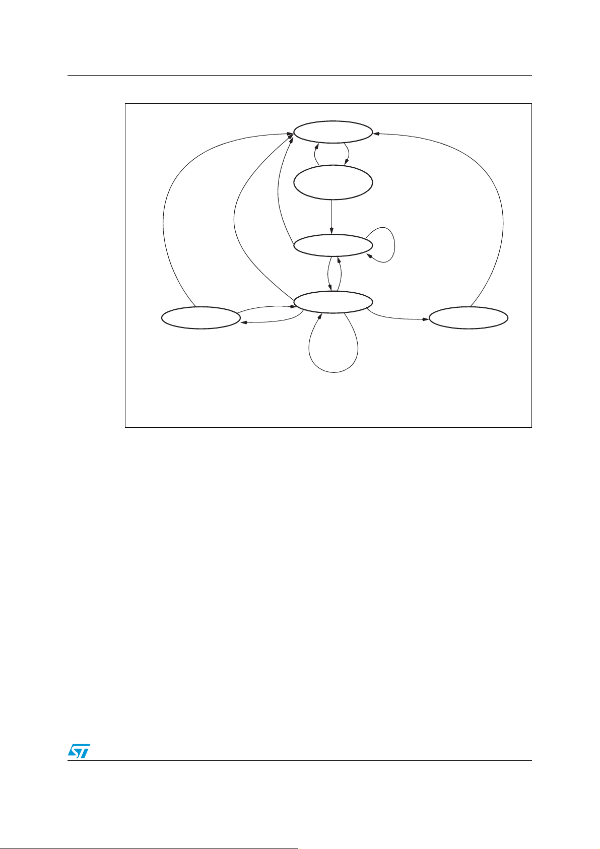
SRI4K provides 6 different states, as described in the following paragraphs and in Figure 19.
6.1 Power-off state
The SRI4K is in Power-off state when the electromagnetic field around the tag is not strong
enough. In this state, the SRI4K does not respond to any command.
6.2 Ready state
When the electromagnetic field is strong enough, the SRI4K enters the Ready state. After
Power-up, the Chip_ID is initialized with a random value. The whole logic is reset and
remains in this state until an Initiate() command is issued. Any other command will be
ignored by the SRI4K.
6.3 Inventory state
The SRI4K switches from the Ready to the Inventory state after an Initiate() command has
been issued. In Inventory state, the SRI4K will respond to any anticollision commands:
Initiate(), Pcall16() and Slot_marker(), and then remain in the Inventory state. It will switch to
the Selected state after a Select(Chip_ID) command is issued, if the Chip_ID in the
command matches its own. If not, it will remain in Inventory state.
6.4 Selected state
In Selected state, the SRI4K is active and responds to all Read_block(), Write_block() and
Get_UID() commands. When an SRI4K has entered the Selected state, it no longer
responds to anticollision commands. So that the reader can access another tag, the SRI4K
can be switched to the Deselected state by sending a Select(Chip_ID2) with a Chip_ID that
does not match its own, or it can be placed in Deactivated state by issuing a Completion()
command. Only one SRI4K can be in Selected state at a time.
6.5 Deselected state
Once the SRI4K is in Deselected state, only a Select(Chip_ID) command with a Chip_ID
matching its own can switch it back to Selected state. All other commands are ignored.
6.6 Deactivated state
When in this state, the SRI4K can only be turned off. All commands are ignored.
20/46 Doc 11605 Rev 5
Page 21
SRI4K SRI4K states
Power-off
Ready
On field
Out of
field
Chip_ID
8bits
= RND
Inventory
Initiate()
Initiate() or Pcall16()
or Slot_marker(SN) or
Select(wrong Chip_ID)
Out of
field
Select(Chip_ID)
Selected
Out of
field
Deselected Deactivated
Select(
≠ Chip_ID)
Select(Chip_ID)
Completion()
Out of
field
Out of
field
Read_block()
Write_block()
Get_UID()
Reset_to_inventory()
Select(Chip_ID)
AI10879b
Figure 19. State transition diagram
Doc 11605 Rev 5 21/46
Page 22

Anticollision SRI4K
ai07668b
b7 b6 b5 b4 b3 b2 b1 b0
8-bit Chip_ID
b0 to b3: Chip_slot_number
7 Anticollision
The SRI4K provides an anticollision mechanism that searches for the Chip_ID of each
device that is present in the reader field range. When known, the Chip_ID is used to select
an SRI4K individually, and access its memory. The anticollision sequence is managed by
the reader through a set of commands described in Section 5: SRI4K operation:
● Initiate()
● Pcall16()
● Slot_marker().
The reader is the master of the communication with one or more SRI4K device(s). It initiates
the tag communication activity by issuing an Initiate(), Pcall16() or Slot_marker() command
to prompt the SRI4K to answer. During the anticollision sequence, it might happen that two
or more SRI4K devices respond simultaneously, so causing a collision. The command set
allows the reader to handle the sequence, to separate SRI4K transmissions into different
time slots. Once the anticollision sequence has completed, SRI4K communication is fully
under the control of the reader, allowing only one SRI4K to transmit at a time.
The Anticollision scheme is based on the definition of time slots during which the SRI4K
devices are invited to answer with minimum identification data: the Chip_ID. The number of
slots is fixed at 16 for the Pcall16() command. For the Initiate() command, there is no slot
and the SRI4K answers after the command is issued. SRI4K devices are allowed to answer
only once during the anticollision sequence. Consequently, even if there are several SRI4K
devices present in the reader field, there will probably be a slot in which only one SRI4K
answers, allowing the reader to capture its Chip_ID. Using the Chip_ID, the reader can then
establish a communication channel with the identified SRI4K. The purpose of the
anticollision sequence is to allow the reader to select one SRI4K at a time.
The SRI4K is given an 8-bit Chip_ID value used by the reader to select only one among up
to 256 tags present within its field range. The Chip_ID is initialized with a random value
during the Ready state, or after an Initiate() command in the Inventory state.
The four least significant bits (
b0 to b
) of the Chip_ID are also known as the
3
Chip_slot_number. This 4-bit value is used by the Pcall16() and Slot_marker() commands
during the anticollision sequence in the Inventory state.
Figure 20. SRI4K Chip_ID description
Each time the SRI4K receives a Pcall16() command, the Chip_slot_number is given a new
4-bit random value. If the new value is 0000
, the SRI4K returns its whole 8-bit Chip_ID in its
b
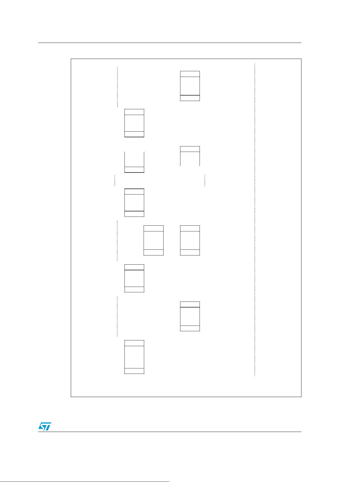
answer to the Pcall16() command. The Pcall16() command is also used to define the slot
number 0 of the anticollision sequence. When the SRI4K receives the Slot_marker(SN)
command, it compares its Chip_slot_number with the Slot_number parameter (SN). If they
match, the SRI4K returns its Chip_ID as a response to the command. If they do not, the
SRI4K does not answer. The Slot_marker(SN) command is used to define all the
anticollision slot numbers from 1 to 15.
22/46 Doc 11605 Rev 5
Page 23
SRI4K Anticollision
Slot 0 Slot 1 Slot 2 Slot N Slot 15
<><>
<
>
Reader
SRI devices
SOF
EOF
<-> <-> <-> <-> < > <-> <-> <->
Timing
t
0
+ t
1
t
2
t
0
+ t
1
t
2
t
3
t
0
+ t
1
Comment
No
collision
Time
>
Ai10883
<>
Collision
No
Answer
t
2
No
collision
t
2
...
Answer
Chip_ID
X1h
EOF
EOF
EOF
Answer
Chip_ID
X0h
Answer
Chip_ID
XFh
SOF
SOF
SOF
SOF
SOF
SOF
EOF
EOF
EOF
EOF
SOF
SOF
EOF
PCALL 16
Request
Slot
Marker
(1)
Slot
Marker
(2)
Answer
Chip_ID
X1h
Slot
Marker
(15)
...
Figure 21. Description of a possible anticollision sequence
1. The value X in the answer Chip_ID means a random hexadecimal character from 0 to F.
Doc 11605 Rev 5 23/46
Page 24

Anticollision SRI4K
7.1 Description of an anticollision sequence
The anticollision sequence is initiated by the Initiate() command which triggers all the SRI4K
devices that are present in the reader field range, and that are in Inventory state. Only
SRI4K devices in Inventory state will respond to the Pcall16() and Slot_marker(SN)
anticollision commands.
A new SRI4K introduced in the field range during the anticollision sequence will not be taken
into account as it will not respond to the Pcall16() or Slot_marker(SN) command (Ready
state). To be considered during the anticollision sequence, it must have received the
Initiate() command and entered the Inventory state.
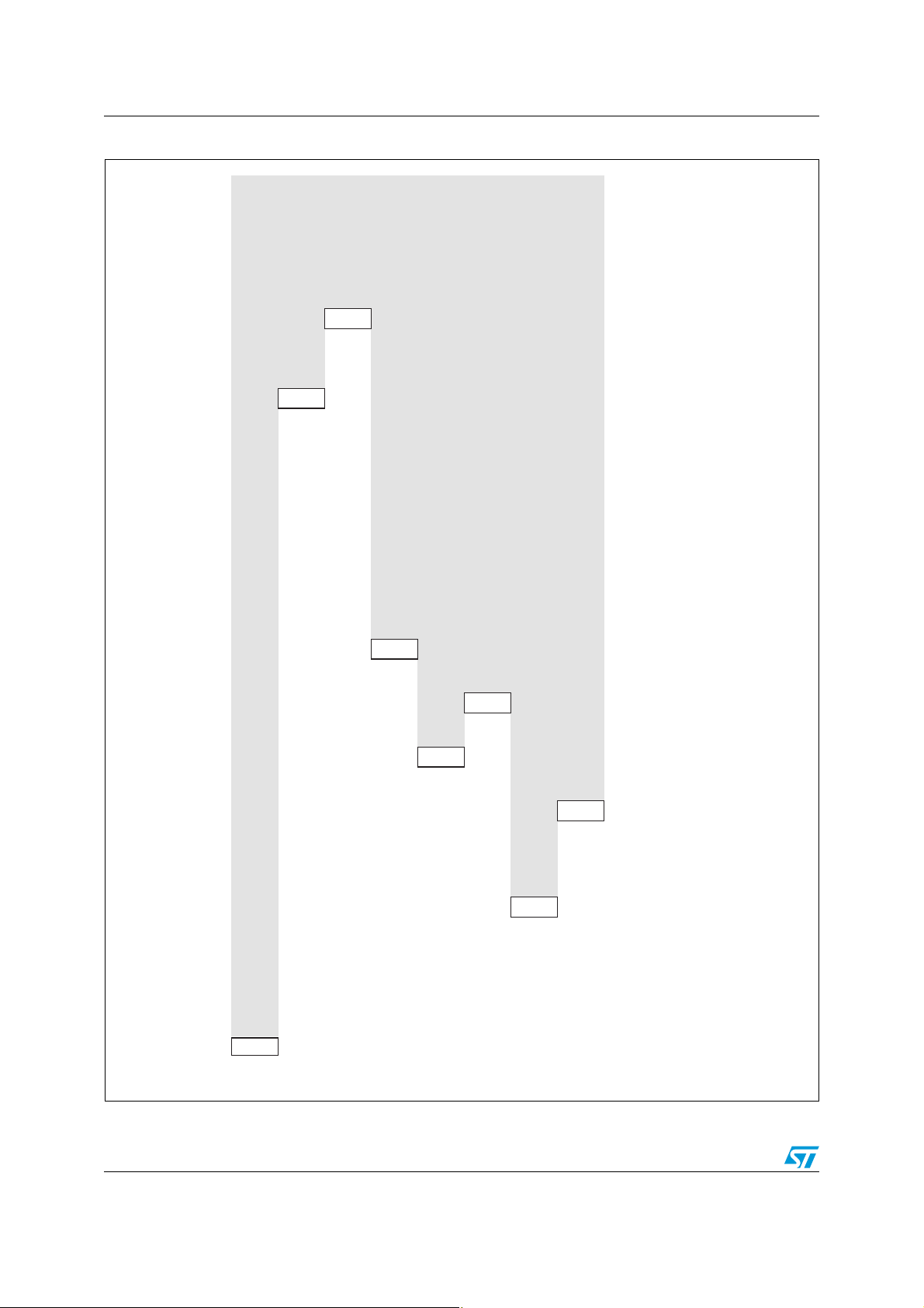
Ta bl e 4 shows the elements of a standard anticollision sequence. (See Figure 22 for an
example.)
Table 4. Standard anticollision sequence
Send Initiate().
– If no answer is detected, go to step1.
Step 1 Init:
Step 2 Slot 0
Step 3 Slot 1
Step 4 Slot 2
– If only 1 answer is detected, select and access the SRI4K. After accessing the
SRI4K, deselect the tag and go to step1.
– If a collision (many answers) is detected, go to step2.
Send Pcall16().
– If no answer or collision is detected, go to step3.
– If 1 answer is detected, store the Chip_ID, Send Select() and go to step3.
Send Slot_marker(1).
– If no answer or collision is detected, go to step4.
– If 1 answer is detected, store the Chip_ID, Send Select() and go to step4.
Send Slot_marker(2).
– If no answer or collision is detected, go to step5.
– If 1 answer is detected, store the Chip_ID, Send Select() and go to step5.
Send Slot_marker(3 up to 14) ...
Step N Slop N
Step 17 Slot 15
Step 18
– If no answer or collision is detected, go to stepN+1.
– If 1 answer is detected, store the Chip_ID, Send Select() and go to stepN+1.
Send Slot_marker(15).
– If no answer or collision is detected, go to step18.
– If 1 answer is detected, store the Chip_ID, Send Select() and go to step18.
All the slots have been generated and the Chip_ID values should be stored into
the reader memory. Issue the Select(Chip_ID) command and access each
identified SRI4K one by one. After accessing each SRI4K, switch them into
Deselected or Deactivated state, depending on the application needs.
– If collisions were detected between Step2 and Step17, go to Step2.
– If no collision was detected between Step2 and Step17, go to Step1.
After each Slot_marker() command, there may be several, one or no answers from the
SRI4K devices. The reader must handle all the cases and store all the Chip_IDs, correctly
decoded. At the end of the anticollision sequence, after Slot_marker(15), the reader can
start working with one SRI4K by issuing a Select() command containing the desired
Chip_ID. If a collision is detected during the anticollision sequence, the reader has to
24/46 Doc 11605 Rev 5
Page 25

SRI4K Anticollision
generate a new sequence in order to identify all unidentified SRI4K devices in the field. The
anticollision sequence can stop when all SRI4K devices have been identified.
Doc 11605 Rev 5 25/46
Page 26
Anticollision SRI4K
Command
Tag 1
Chip_ID
Tag 2
Chip_ID
Tag 3
Chip_ID
Tag 4
Chip_ID
Tag 5
Chip_ID
Tag 6
Chip_ID
Tag 7
Chip_ID
Tag 8
Chip_ID
Comments
READY State
28h 75h 40h 01h 02h FEh A9h 7Ch
Each tag gets a random Chip_ID
INITIATE ()
40h 13h 3Fh 4Ah 50h 48h 52h 7Ch
Each tag get a new random Chip_ID.
All tags answer: collisions
45h 12h 30h 43h 55h 43h 53h 73h
All CHIP_SLOT_NUMBERs get
a new random value
PCALL16()
30h
Slot0: only one answer
30h Tag3 is identifiedSELECT(30h)
SLOT_MARKER(1) Slot1: no answer
SLOT_MARKER(2) Slot2: only one answer12h
12h Tag2 is identifiedSELECT(12h)
SLOT_MARKER(3) Slot3: collisions
SLOT_MARKER(4) Slot4: no answer
43h 43h 53h 73h
SLOT_MARKER(5) Slot5: collisions
SLOT_MARKER(6) Slot6: no answer
45h 55h
SLOT_MARKER(N) SlotN: no answer
SLOT_MARKER(F) SlotF: no answer
40h 41h 53h 42h 50h 74h
All CHIP_SLOT_NUMBERs get
a new random value
PCALL16()
40h Slot0: collisions
SLOT_MARKER(1) Slot1: only one answer
SLOT_MARKER(2) Slot2: only one answer
42h Tag6 is identifiedSELECT(42h)
SLOT_MARKER(3) Slot3: only one answer
SELECT(53h) Tag5 is identified
53h
SLOT_MARKER(4) Slot4: only one answer
SELECT(74h) Tag8 is identified
74h
SLOT_MARKER(N) SlotN: no answer
50h
41h Tag4 is identifiedSELECT(41h)
41h
42h
53h
74h
41h 50h
All CHIP_SLOT_NUMBERs get
a new random value
PCALL16()
Slot0: only one answer
50h Tag7 is identifiedSELECT(50h)
SLOT_MARKER(1)
Slot1: only one answer but already
found for tag4
SLOT_MARKER(N)
SlotN: no answer
50h
41h
43h
All CHIP_SLOT_NUMBERs get
a new random valuePCALL16()
Slot0: only one answer
SLOT_MARKER(3) Slot3: only one answer
43h
Tag1 is identifiedSELECT(43h)
43h
All tags are identified
ai07669
Figure 22. Example of an anticollision sequence
26/46 Doc 11605 Rev 5
Page 27
SRI4K SRI4K commands
8 SRI4K commands
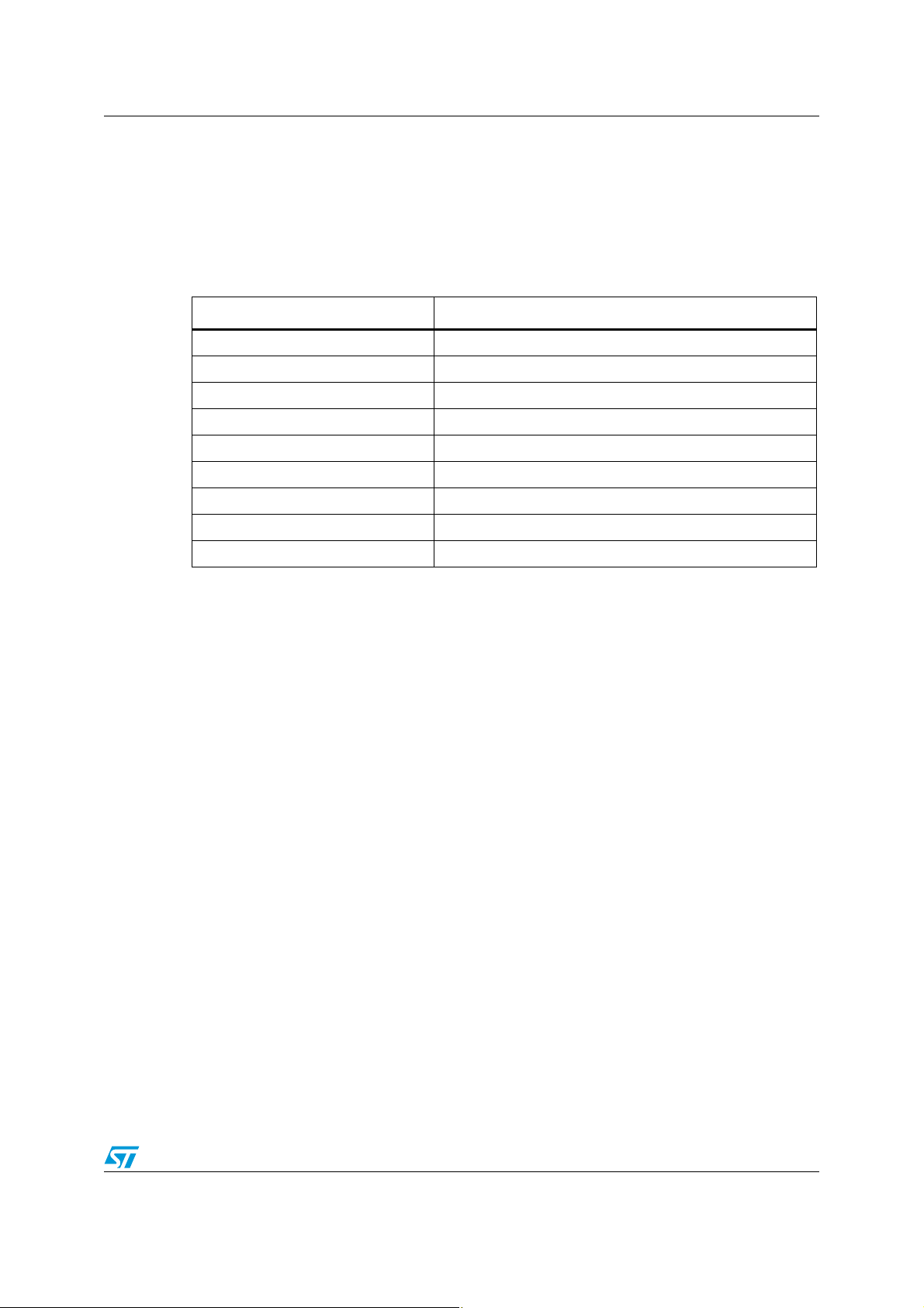
See the paragraphs below for a detailed description of the commands available on the
SRI4K. The commands and their hexadecimal codes are summarized in Ta bl e 5 . A brief is
given in Appendix B.
Table 5. Command code
Hexadecimal code Command
06h-00h Initiate()
06h-04h Pcall16()
x6h Slot_marker (SN)
08h Read_block(Addr)
09h Write_block(Addr, Data)
0Bh Get_UID()
0Ch Reset_to_inventory
0Eh Select(Chip_ID)
0Fh Completion()
Doc 11605 Rev 5 27/46
Page 28
SRI4K commands SRI4K
SOF Initiate CRC
L
CRC
H
EOF
AI07670b
06h 00h 8 bits 8 bits
SOF Chip_ID CRC
L
CRC
H
EOF
AI07671
8 bits 8 bits 8 bits
AI10884b
Reader
SRI4K
SOF Chip_ID CRCLCRCHEOF
<-t0-><-t1->
SOF 06h CRCLCRCHEOF00h
8.1 Initiate() command
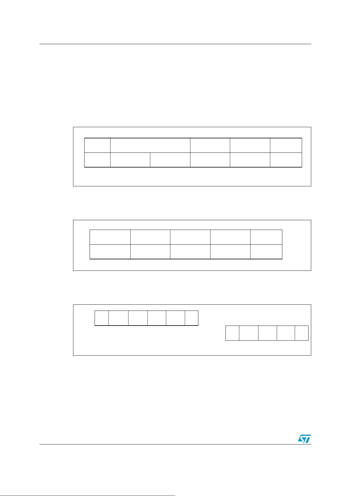
Command code = 06h - 00h
Initiate() is used to initiate the anticollision sequence of the SRI4K. On receiving the Initiate()
command, all SRI4K devices in Ready state switch to Inventory state, set a new 8-bit
Chip_ID random value, and return their Chip_ID value. This command is useful when only
one SRI4K in Ready state is present in the reader field range. It speeds up the Chip_ID
search process. The Chip_slot_number is not used during Initiate() command access.
Figure 23. Initiate request format
Request parameter:
● No parameter
Figure 24. Initiate response format
Response parameter:
● Chip_ID of the SRI4K
Figure 25. Initiate frame exchange between reader and SRI4K
28/46 Doc 11605 Rev 5
Page 29
SRI4K SRI4K commands
SOF Pcall16 CRC
L
CRC
H
EOF
AI07673b
06h 04h 8 bits 8 bits
SOF Chip_ID CRC
L
CRC
H
EOF
AI07671
8 bits 8 bits 8 bits
SOF 06h CRCLCRCHEOF
AI10885b
Reader
SRI4K
SOF Chip_ID CRCLCRCHEOF
<-t0-><-t1->
04h
8.2 Pcall16() command
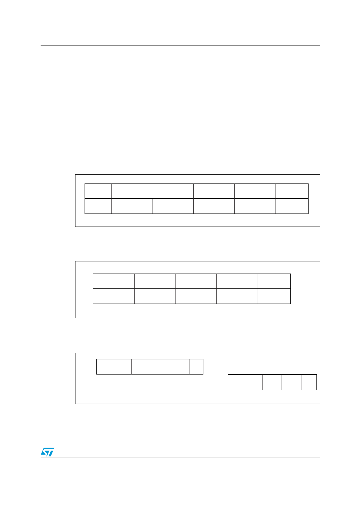
Command code = 06h - 04h
The SRI4K must be in Inventory state to interpret the Pcall16() command.
On receiving the Pcall16() command, the SRI4K first generates a new random
Chip_slot_number value (in the 4 least significant bits of the Chip_ID). Chip_slot_number
can take on a value between 0 an 15 (1111
Initiate() command is issued, or until the SRI4K is powered off. The new Chip_slot_number
value is then compared with the value 0000
value. If not, the SRI4K does not send any response.
The Pcall16() command, used together with the Slot_marker() command, allows the reader
to search for all the Chip_IDs when there are more than one SRI4K device in Inventory state
present in the reader field range.
Figure 26. Pcall16 request format
). The value is retained until a new Pcall16() or
b
. If they match, the SRI4K returns its Chip_ID
b
Request parameter:
● No parameter
Figure 27. Pcall16 response format
Response parameter:
● Chip_ID of the SRI4K
Figure 28. Pcall16 frame exchange between reader and SRI4K
Doc 11605 Rev 5 29/46
Page 30
SRI4K commands SRI4K
SOF Slot_marker CRC
L
CRC
H
EOF
AI07675b
X6h 8 bits 8 bits
SOF Chip_ID CRC
L
CRC
H
EOF
AI07671
8 bits 8 bits 8 bits
SOF X6h CRCLCRCHEOF
AI10886
Reader
SRI4K
SOF Chip_ID CRCLCRCHEOF
<-t0-><-t1->
8.3 Slot_marker(SN) command
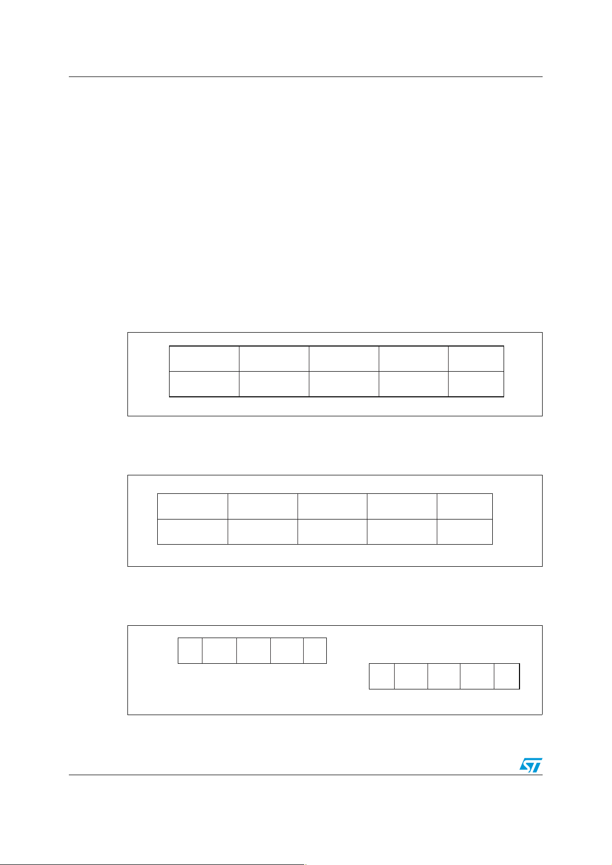
Command code = x6h
The SRI4K must be in Inventory state to interpret the Slot_marker(SN) command.
The Slot_marker byte code is divided into two parts:
● b
● b
On receiving the Slot_marker() command, the SRI4K compares its Chip_slot_number value
with the Slot_number value given in the command code. If they match, the SRI4K returns its
Chip_ID value. If not, the SRI4K does not send any response.
The Slot_marker() command, used together with the Pcall16() command, allows the reader
to search for all the Chip_IDs when there are more than one SRI4K device in Inventory state
present in the reader field range.
Figure 29. Slot_marker request format
to b0: 4-bit command code
3
with fixed value 6.
to b4: 4 bits known as the Slot_number (SN). They assume a value between 1 and
7
15. The value 0 is reserved by the Pcall16() command.
Request parameter:
● x: Slot number
Figure 30. Slot_marker response format
Response parameters:
● Chip_ID of the SRI4K
Figure 31. Slot_marker frame exchange between reader and SRI4K
30/46 Doc 11605 Rev 5
Page 31
SRI4K SRI4K commands
SOF Select CRC
L
CRC
H
EOF
AI07677b
0Eh 8 bits 8 bits 8 bits
Chip_ID
SOF Chip_ID CRC
L
CRC
H
EOF
AI07671
8 bits 8 bits 8 bits
AI010887
Reader
SRI4K
SOF Chip_ID CRCLCRCHEOF
<-t0-><-t1->
SOF 0Eh CRCLCRCHEOFChip_ID
8.4 Select(Chip_ID) command
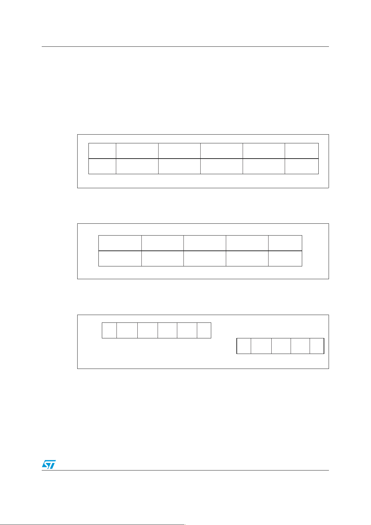
Command code = 0Eh
The Select() command allows the SRI4K to enter the Selected state. Until this command is
issued, the SRI4K will not accept any other command, except for Initiate(), Pcall16() and
Slot_marker(). The Select() command returns the 8 bits of the Chip_ID value. An SRI4K in
Selected state, that receives a Select() command with a Chip_ID that does not match its
own is automatically switched to Deselected state.
Figure 32. Select request format
Request parameter:
● 8-bit Chip_ID stored during the anticollision sequence
Figure 33. Select response format
Response parameters:
● Chip_ID of the selected tag. Must be equal to the transmitted Chip_ID
Figure 34. Select frame exchange between reader and SRI4K
Doc 11605 Rev 5 31/46
Page 32
SRI4K commands SRI4K
SOF Completion CRC
L
CRC
H
EOF
AI07679b
0Fh 8 bits 8 bits
AI07680
No Response
SOF 0Fh CRCLCRCHEOF
AI10888
Reader
SRI4K
No Response
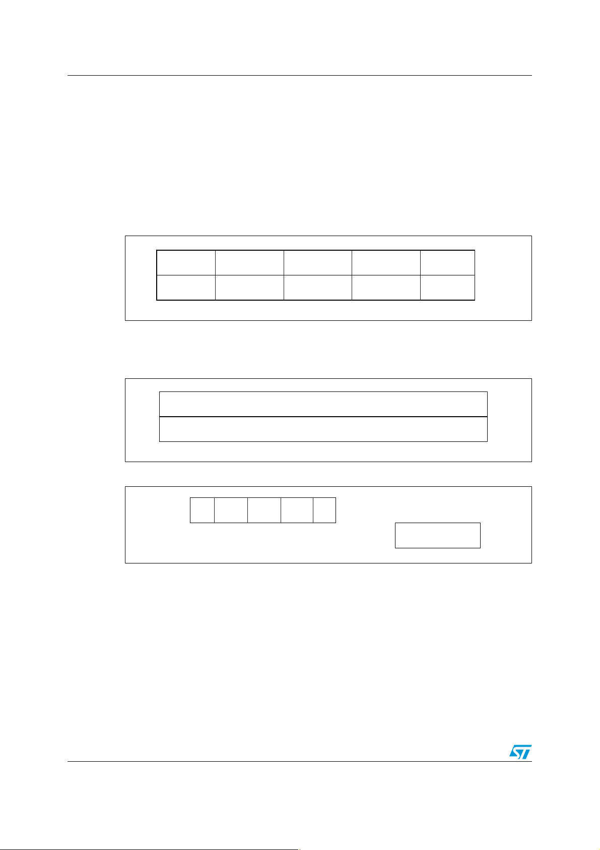
8.5 Completion() command
Command code = 0Fh
On receiving the Completion() command, an SRI4K in Selected state switches to
Deactivated state and stops decoding any new commands. The SRI4K is then locked in this
state until a complete reset (tag out of the field range). A new SRI4K can thus be accessed
through a Select() command without having to remove the previous one from the field. The
Completion() command does not generate a response.
All SRI4K devices not in Selected state ignore the Completion() command.
Figure 35. Completion request format
Request parameters:
● No parameter
Figure 36. Completion response format
Figure 37. Completion frame exchange between reader and SRI4K
32/46 Doc 11605 Rev 5
Page 33
SRI4K SRI4K commands
SOF RESET_TO_INVENTORY CRC
L
CRC
H
EOF
AI07682
0Ch 8 bits 8 bits
AI07680
No Response
SOF 0Ch CRCLCRCHEOF
AI10889
Reader
SRI4K
No Response
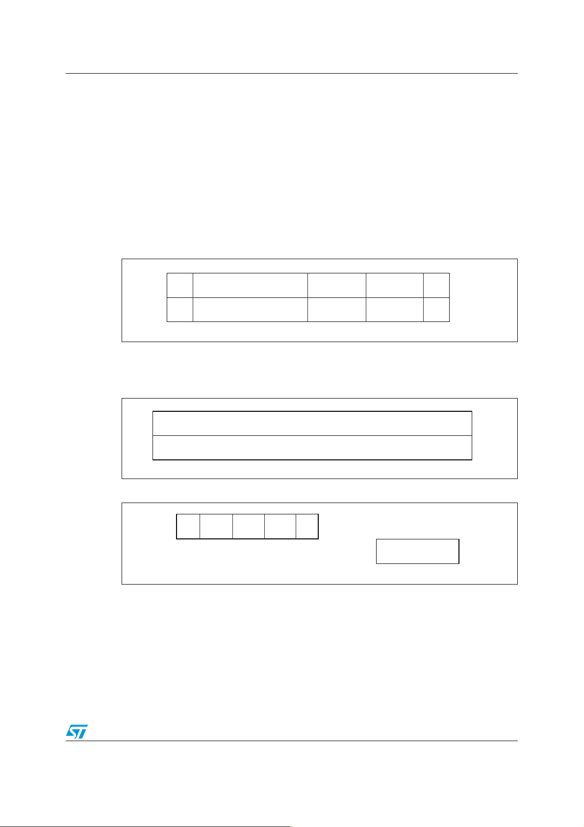
8.6 Reset_to_inventory() command
Command code = 0Ch
On receiving the Reset_to_inventory() command, all SRI4K devices in Selected state revert
to Inventory state. The concerned SRI4K devices are thus resubmitted to the anticollision
sequence. This command is useful when two SRI4K devices with the same 8-bit Chip_ID
happen to be in Selected state at the same time. Forcing them to go through the anticollision
sequence again allows the reader to generates new Pcall16() commands and so, to set new
random Chip_IDs.
The Reset_to_inventory() command does not generate a response.
All SRI4K devices that are not in Selected state ignore the Reset_to_inventory() command.
Figure 38. Reset_to_inventory request format
Request parameter:
● No parameter
Figure 39. Reset_to_inventory response format
Figure 40. Reset_to_inventory frame exchange between reader and SRI4K
Doc 11605 Rev 5 33/46
Page 34
SRI4K commands SRI4K
SOF Read_block CRC
L
CRC
H
EOF
AI07684b
08h 8 bIts 8 bits 8 bits
Address
SOF Data 1 CRC
L
CRC
H
EOF
AI07685b
8 bits
Data 2 Data 3 Data 4
8 bIts 8 bIts 8 bIts 8 bIts 8 bIts
S
O
F
Data 1
AI10890c
Data 2 Data 3 Data 4
Reader
SRI4K
CRCLCRC
H
E
O
F
<-t0-><-t1->
S
O
F
08h CRCLCRC
H
E
O
F
Address
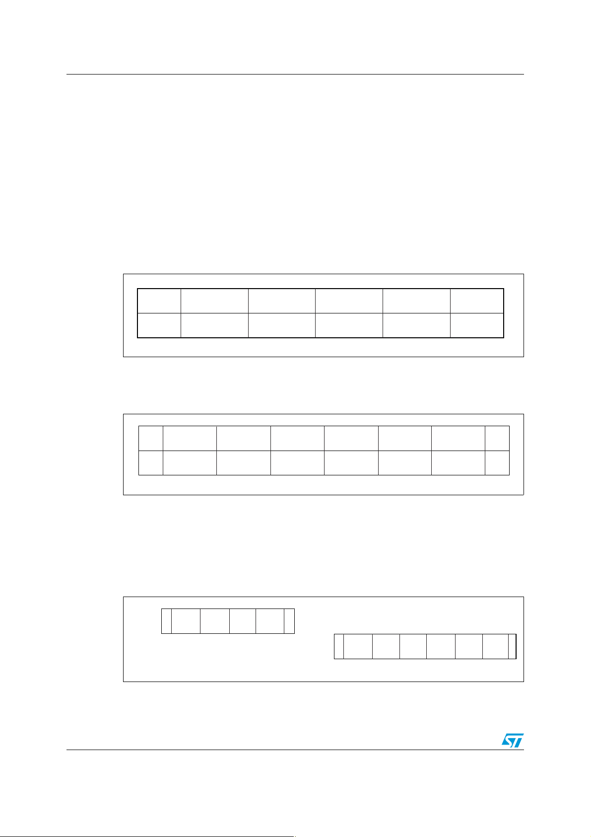
8.7 Read_block(Addr) command
Command code = 08h
On receiving the Read_block command, the SRI4K reads the desired block and returns the
4 data bytes contained in the block. Data bytes are transmitted with the least significant byte
first and each byte is transmitted with the least significant bit first.
The address byte gives access to the 128 blocks of the SRI4K (addresses 0 to 127).
Read_block commands issued with a block address above 127 will not be interpreted and
the SRI4K will not return any response, except for the System area located at address 255.
The SRI4K must have received a Select() command and be switched to Selected state
before any Read_block() command can be accepted. All Read_block() commands sent to
the SRI4K before a Select() command is issued are ignored.
Figure 41. Read_block request format
Request parameter:
● Address: block addresses from 0 to 127, or 255
Figure 42. Read_block response format
Response parameters:
● Data 1: Less significant data byte
● Data 2: Data byte
● Data 3: Data byte
● Data 4: Most significant data byte
Figure 43. Read_block frame exchange between reader and SRI4K
34/46 Doc 11605 Rev 5
Page 35
SRI4K SRI4K commands
SOF Data 1 CRC
L
CRCHEOF
AI07687b
8 bits
Data 2 Data 3 Data 4
8 bIts 8 bIts 8 bIts 8 bIts 8 bIts
Write_block Address
09h
8 bIts
AI07680b
No response
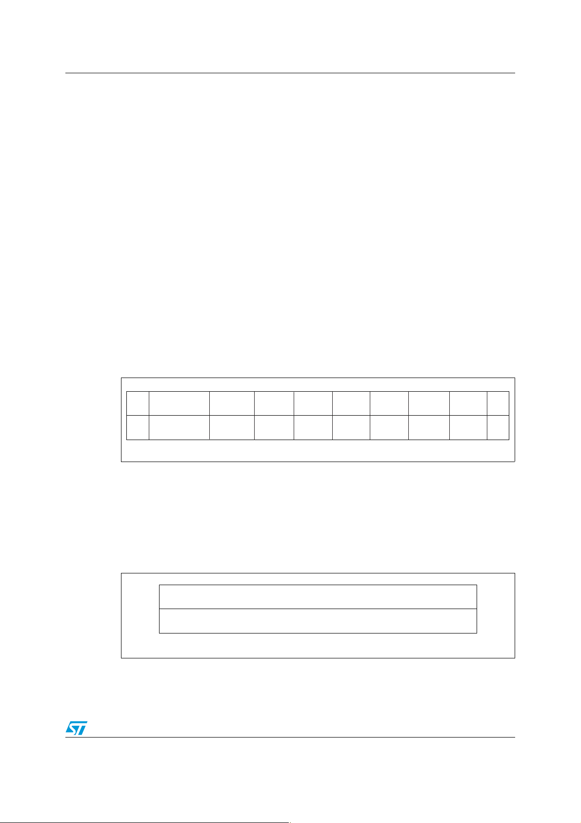
8.8 Write_block (Addr, Data) command
Command code = 09h
On receiving the Write_block command, the SRI4K writes the 4 bytes contained in the
command to the addressed block, provided that the block is available and not writeprotected. Data bytes are transmitted with the least significant byte first, and each byte is
transmitted with the least significant bit first.
The address byte gives access to the 128 blocks of the SRI4K (addresses 0 to 127).
Write_block commands issued with a block address above 127 will not be interpreted and
the SRI4K will not return any response, except for the System area located at address 255.
The result of the Write_block command is submitted to the addressed block. See the
following Figures for a complete description of the Write_block command:
● Figure 12: Resettable OTP area (addresses 0 to 4).
● Figure 15: Binary counter (addresses 5 to 6).
● Figure 17: EEPROM (addresses 7 to 127).
The Write_block command does not give rise to a response from the SRI4K. The reader
must check after the programming time, t
SRI4K must have received a Select() command and be switched to Selected state before
any Write_block command can be accepted. All Write_block commands sent to the SRI4K
before a Select() command is issued, are ignored.
, that the data was correctly programmed. The
W
Figure 44. Write_block request format
● Request parameters:
● Address: block addresses from 0 to 127, or 255
● Data 1: Less significant data byte
● Data 2: Data byte
● Data 3: Data byte
● Data 4: Most significant data byte.
Figure 45. Write_block response format
Doc 11605 Rev 5 35/46
Page 36
SRI4K commands SRI4K
Data 1
AI10891b
Data 2 Data 3 Data 4
Reader
SRI4K
CRCLCRCHEOF
SOF 09h
Address
No response
SOF Get_UID CRC
L
CRC
H
EOF
AI07693b
0Bh 8 bits 8 bits
SOF
UID 1 CRCLCRC
H
EOF
AI07694
8 bits
UID 2 UID 3 UID 4
8 bIts 8 bIts 8 bIts 8 bIts 8 bIts
UID 0 UID 5
8 bIts
UID 6
8 bIts8 bits
UID 7
8 bIts
Figure 46. Write_block frame exchange between reader and SRI4K
8.9 Get_UID() command
Command code = 0Bh
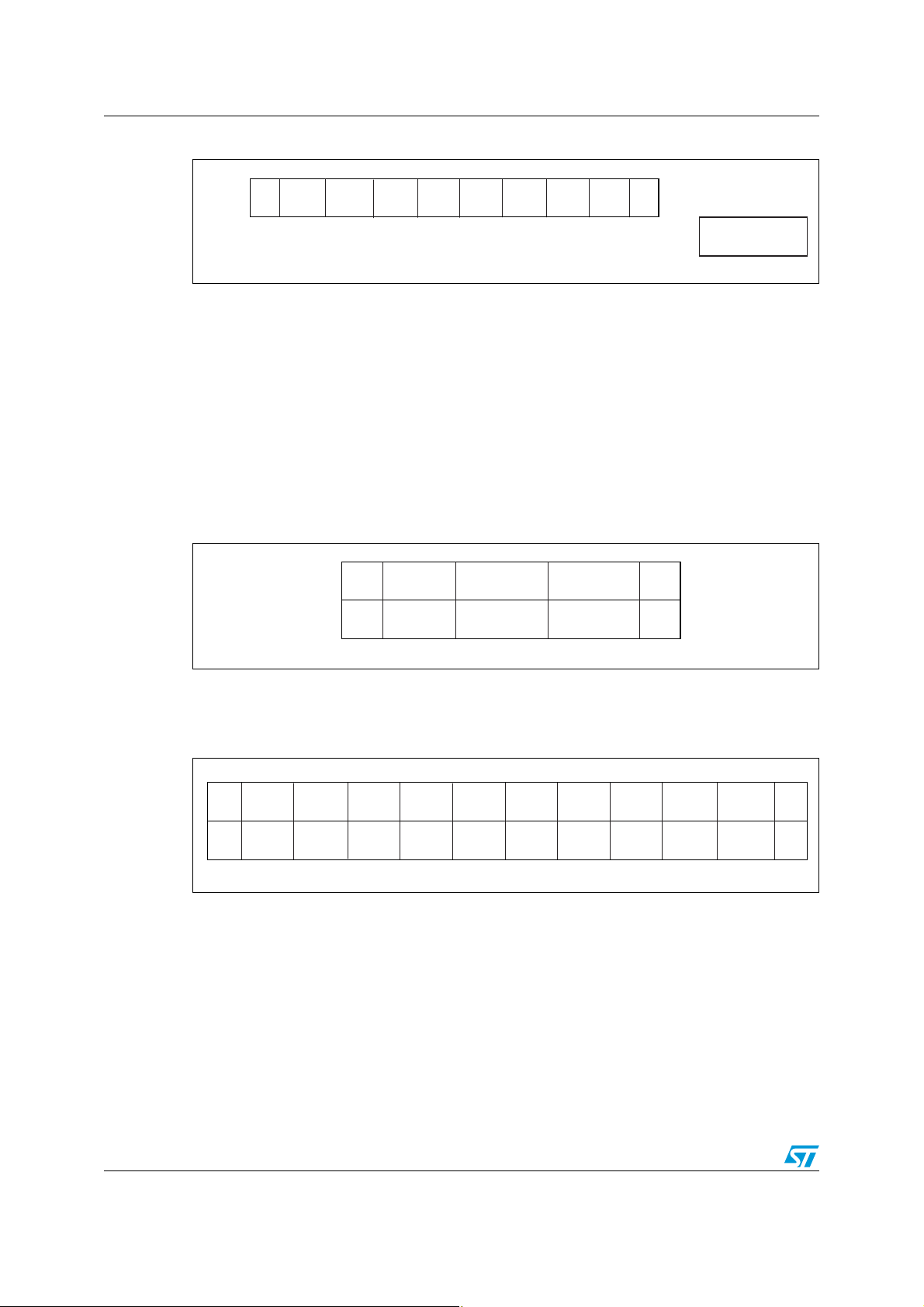
On receiving the Get_UID command, the SRI4K returns its 8 UID bytes. UID bytes are
transmitted with the least significant byte first, and each byte is transmitted with the least
significant bit first.
The SRI4K must have received a Select() command and be switched to Selected state
before any Get_UID() command can be accepted. All Get_UID() commands sent to the
SRI4K before a Select() command is issued, are ignored.
Figure 47. Get_UID request format
Request parameter:
● No parameter
Figure 48. Get_UID response format
Response parameters:
● UID 0: Less significant UID byte
● UID 1 to UID 6: UID bytes
● UID 7: Most significant UID byte.
36/46 Doc 11605 Rev 5
Page 37
SRI4K SRI4K commands
AI14081
D0h Unique Serial Number02h
63 55 47
0
Most significant bits Least significant bits
41
7d
S
O
F
CRCLCRC
H
E
O
F
AI10892b
Reader
SRI4K
<-t0-><-t1->
S
O
F
CRCLCRC
H
E
O
F
0Bh
UID1UID2UID3UID
4
UID
0
UID5UID6UID
7
Unique identifier (UID)
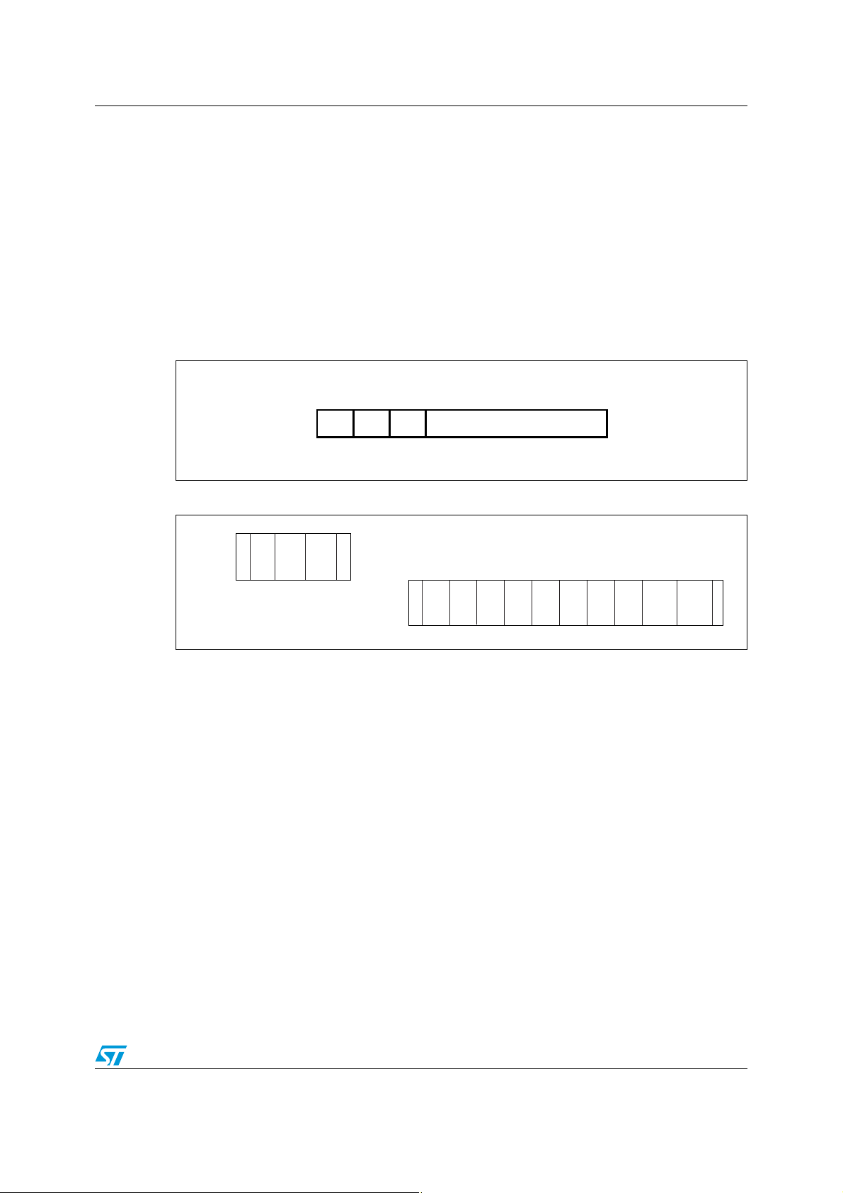
Members of the SRI4K family are uniquely identified by a 64-bit unique identifier (UID). This
is used for addressing each SRI4K device uniquely after the anticollision loop. The UID
complies with ISO/IEC 15963 and ISO/IEC 7816-6. It is a read-only code, and comprises
(as summarized in Figure 49):
● an 8-bit prefix, with the most significant bits set to D0h
● an 8-bit IC manufacturer code (ISO/IEC 7816-6/AM1) set to 02h (for
STMicroelectronics)
● a 6-bit IC code set to 00 0111b = 7d for SRI4K
● a 42-bit unique serial number
Figure 49. 64-bit unique identifier of the SRI4K
Figure 50. Get_UID frame exchange between reader and SRI4K
8.10 Power-on state
After power-on, the SRI4K is in the following state:
● It is in the low-power state.
● It is in Ready state.
● It shows highest impedance with respect to the reader antenna field.
● It will not respond to any command except Initiate().
Doc 11605 Rev 5 37/46
Page 38
Maximum rating SRI4K
9 Maximum rating
Stressing the device above the rating listed in the absolute maximum ratings table may
cause permanent damage to the device. These are stress ratings only and operation of the
device at these or any other conditions above those indicated in the operating sections of
this specification is not implied. Exposure to absolute maximum rating conditions for
extended periods may affect device reliability. Refer also to the STMicroelectronics SURE
Program and other relevant quality documents.
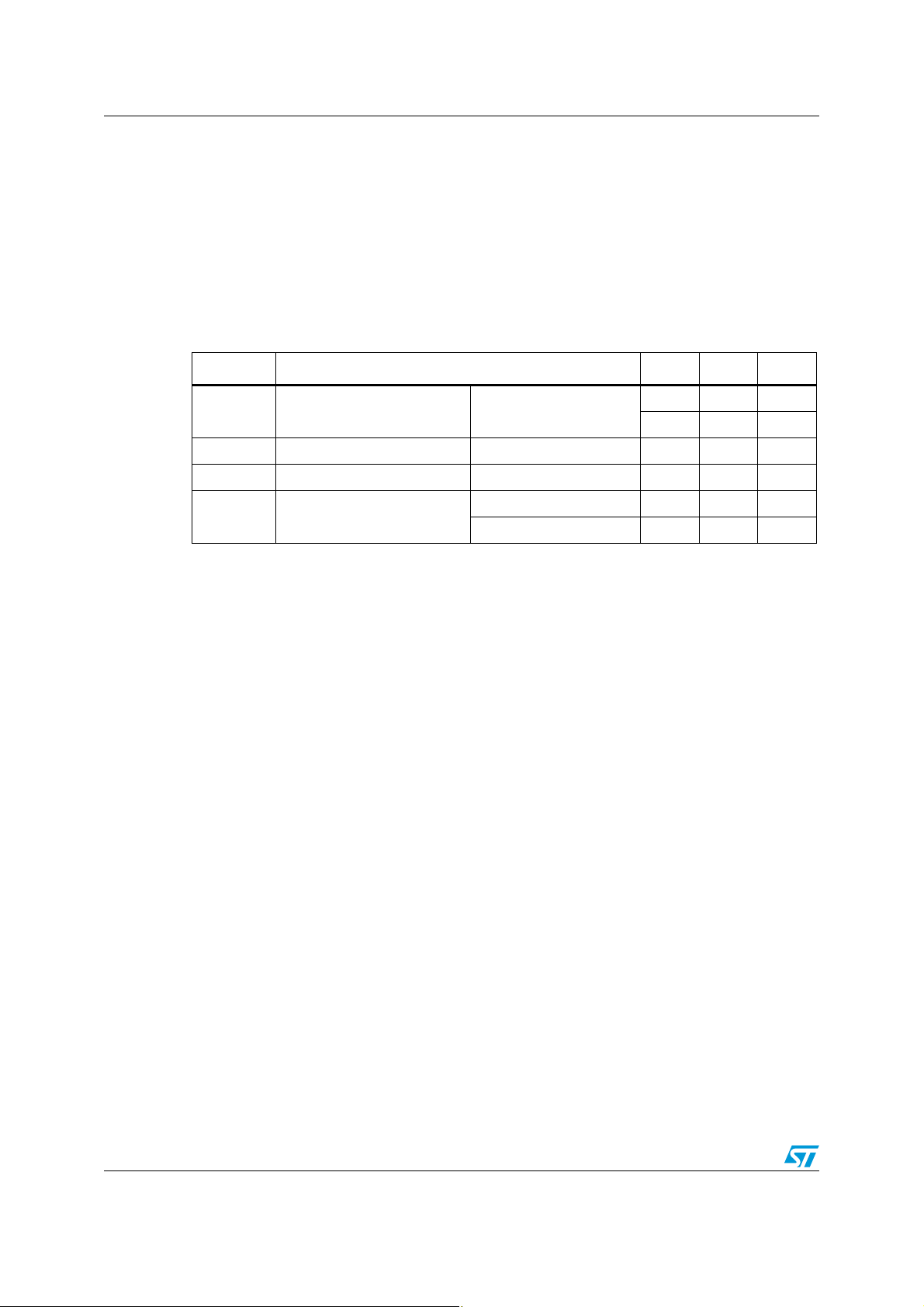
Table 6. Absolute maximum ratings
Symbol Parameter Min. Max. Unit
T
, t
STG
I
CC
V
MAX
V
ESD
1. Mil. Std. 883 - Method 3015
Storage conditions
STG
Supply current on AC0 / AC1 –20 20 mA
Input voltage on AC0 / AC1 –7 7 V
Electrostatic discharge
(1)
voltage
Wafer
(kept in its antistatic bag)
15 25 °C
23 months
Machine model –100 100 V
Human body model –1000 1000 V
38/46 Doc 11605 Rev 5
Page 39
SRI4K DC and ac parameters
10 DC and ac parameters
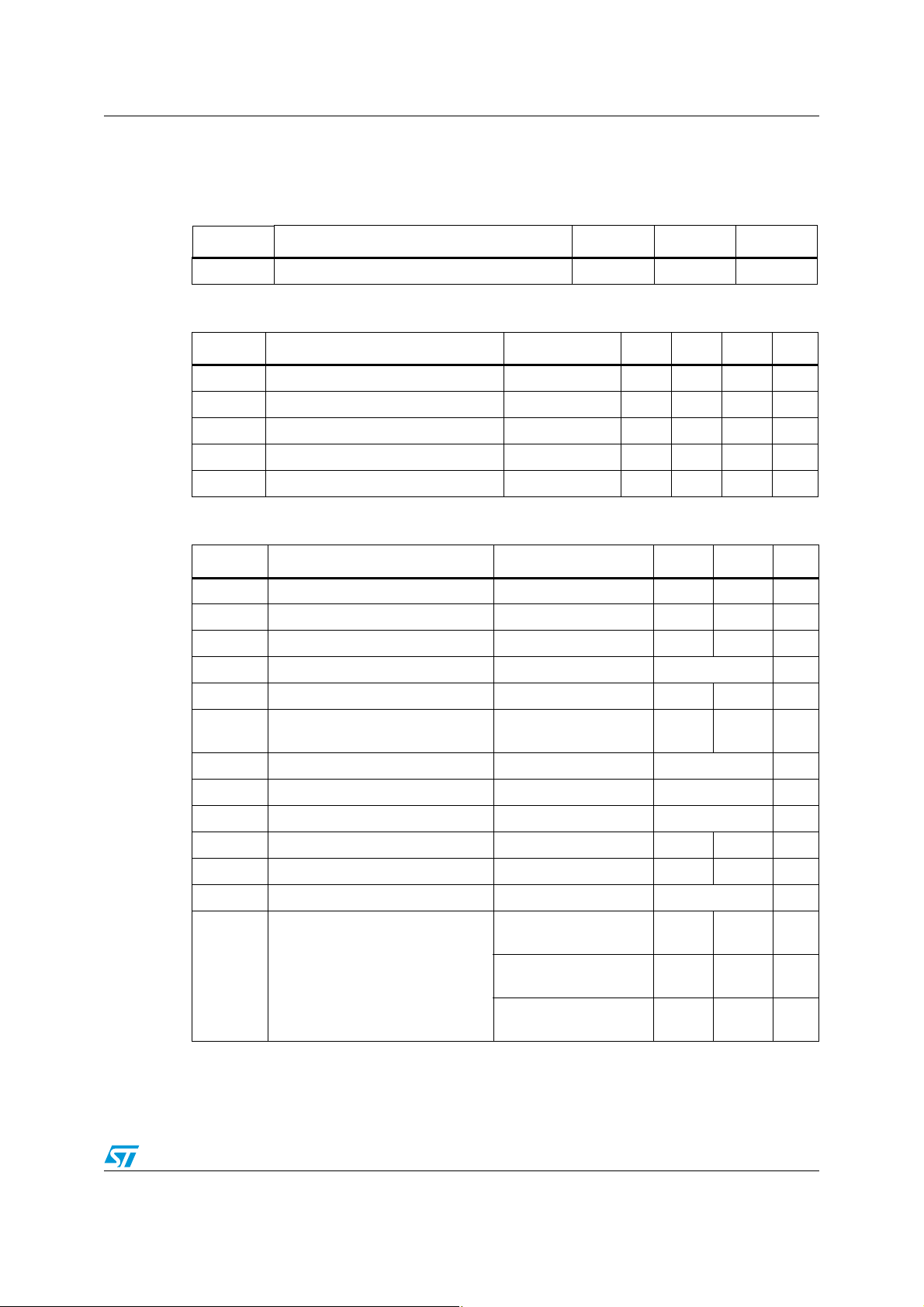
Table 7. Operating conditions
Symbol Parameter Min. Max. Unit
T
A
Table 8. DC characteristics
Ambient operating temperature –20 85 °C
Symbol Parameter Condition Min Typ Max Unit
V
I
CC
I
CC
V
RET
C
TUN
Table 9. AC characteristics
Regulated voltage 2.5 3.5 V
CC
Supply current (active in read) VCC= 3.0 V 100 µA
Supply current (active in write) VCC= 3.0 V 250 µA
Retromodulation induced voltage ISO 10373-6 20 mV
Internal tuning capacitor 13.56 MHz 64 pF
(1)
Symbol Parameter Condition Min Max Unit
f
CC
MI
CARRIER
t
RFR,tRFF
t
RFSBL
t
JIT
t
MIN CD
f
t
t
t
t
DR
t
DA
t
W
External RF signal frequency 13.553 13.567 MHz
Carrier modulation index MI=(A-B)/(A+B) 8 14 %
10% Rise and Fall times 0.8 2.5 µs
Minimum pulse width for Start bit ETU = 128/f
CC
9.44 µs
ASK modulation data jitter Coupler to SRI4K –2 +2 µs
Minimum time from carrier
generation to first data
Subcarrier frequency fCC/16 847.5 kHz
S
Antenna reversal delay 128/f
0
Synchronization delay 128/f
1
Answer to new request delay 14 ETU 132 µs
2
S
S
5ms
151 µs
151 µs
Time between request characters Coupler to SRI4K 0 57 µs
Time between answer characters SRI4K to coupler 0 µs
With no auto-erase
cycle (OTP)
Programming time for write
With auto-erase cycle
(EEPROM)
3ms
5ms
Binary counter
decrement
7ms
Doc 11605 Rev 5 39/46
Page 40
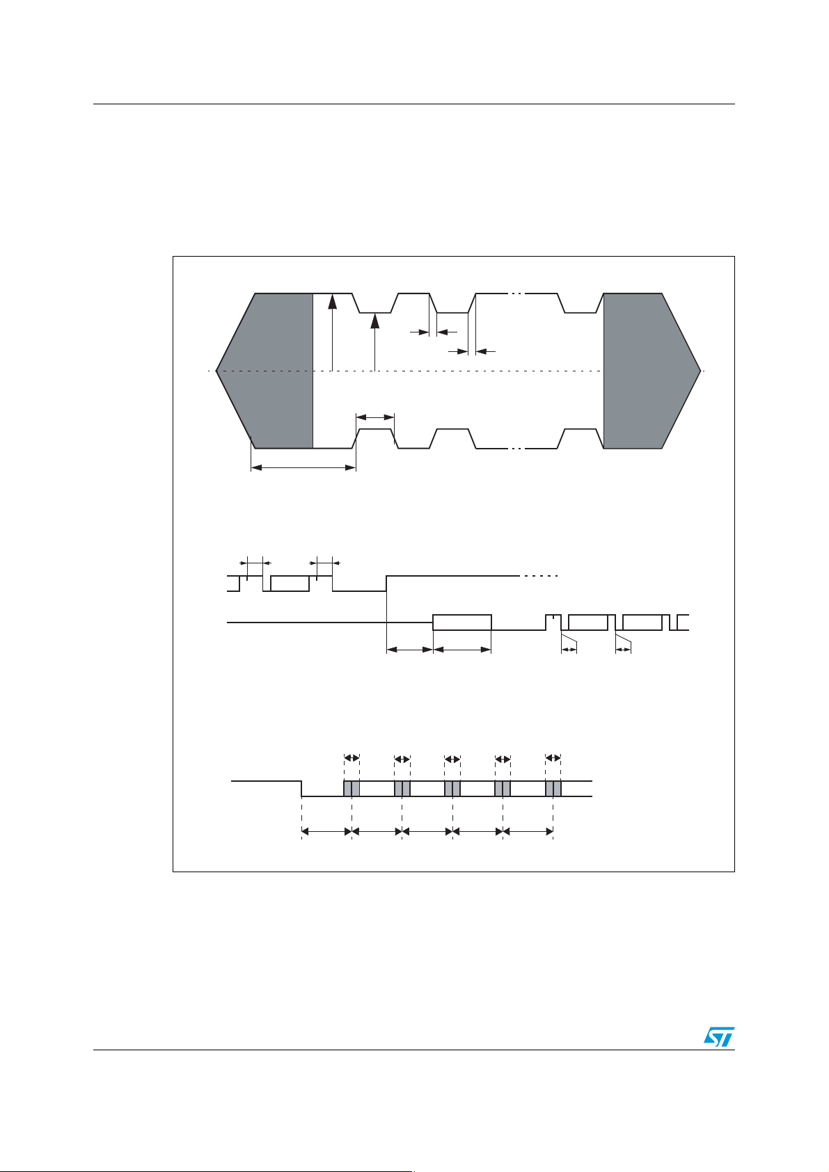
DC and ac parameters SRI4K
AB
t
RFF
t
RFR
t
RFSBL
t
MIN CD
ƒ
cc
ASK Modulated signal from the Reader to the Contactless device
DATA
0
EOF
847KHz
t
DR
t
0
t
1
FRAME Transmission between the reader and the contactless device
FRAME Transmitted by the reader in ASK
FRAME Transmitted by the SRI4K
11
t
DR
in BPSK
DATA
0
1
DATA
0
t
DA
t
DA
SOF
1
0
1 1
START
0
t
RFSBLtRFSBLtRFSBL
t
JIT
t
JIT
t
JIT
t
JIT
t
JIT
t
RFSBLtRFSBL
Data jitter on FRAME Transmitted by the reader in ASK
AI10893
1. All timing measurements were performed on a reference antenna with the following characteristics:
External size: 75 mm x 48 mm
Number of turns: 3
Width of conductor: 1 mm
Space between 2 conductors: 0.4 mm
Value of the coil: 1.4 µH
Tuning Frequency: 14.4 MHz.
Figure 51. SRI4K synchronous timing, transmit and receive
40/46 Doc 11605 Rev 5
Page 41

SRI4K Part numbering
11 Part numbering
Table 10. Ordering information scheme
Example: SRI4K – W4 /1GE
Device type
SRI4K
Package
W4 = 180 µm ± 15 µm unsawn wafer
SBN18 = 180 µm ± 15 µm bumped and sawn wafer on 8-inch frame
Customer code
1GE = generic product
xxx = customer code after personalization
Note: Devices are shipped from the factory with the memory content bits erased to 1.
For a list of available options (speed, package, etc.) or for further information on any aspect
of this device, please contact your nearest ST sales office.
Doc 11605 Rev 5 41/46
Page 42

ISO-14443 Type B CRC calculation SRI4K
Appendix A ISO-14443 Type B CRC calculation
#include <stdio.h>
#include <stdlib.h>
#include <string.h>
#include <ctype.h>
#define BYTE unsigned char
#define USHORT unsigned short
unsigned short UpdateCrc(BYTE ch, USHORT *lpwCrc)
{
ch = (ch^(BYTE)((*lpwCrc) & 0x00FF));
ch = (ch^(ch<<4));
*lpwCrc = (*lpwCrc >> 8)^((USHORT)ch <<
8)^((USHORT)ch<<3)^((USHORT)ch>>4);
return(*lpwCrc);
}
void ComputeCrc(char *Data, int Length, BYTE *TransmitFirst, BYTE
*TransmitSecond)
{
BYTE chBlock; USHORTt wCrc;
wCrc = 0xFFFF; // ISO 3309
do
{
chBlock = *Data++;
UpdateCrc(chBlock, &wCrc);
} while (--Length);
wCrc = ~wCrc; // ISO 3309
*TransmitFirst = (BYTE) (wCrc & 0xFF);
*TransmitSecond = (BYTE) ((wCrc >> 8) & 0xFF);
return;
}
int main(void)
{
BYTE BuffCRC_B[10] = {0x0A, 0x12, 0x34, 0x56}, First, Second, i;
printf("Crc-16 G(x) = x^16 + x^12 + x^5 + 1”);
printf("CRC_B of [ ");
for(i=0; i<4; i++)
printf("%02X ",BuffCRC_B[i]);
ComputeCrc(BuffCRC_B, 4, &First, &Second);
printf("] Transmitted: %02X then %02X.”, First, Second);
return(0);
42/46 Doc 11605 Rev 5
Page 43
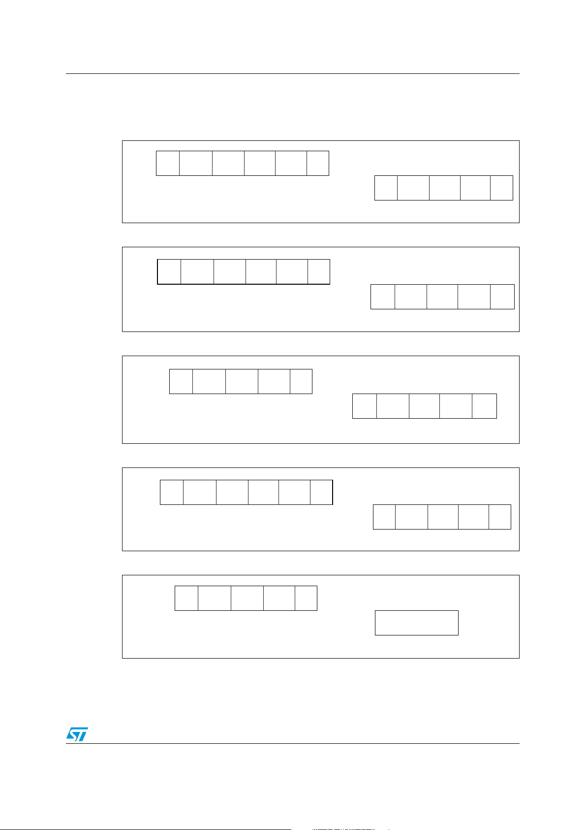
SRI4K SRI4K command summary
AI10884b
Reader
SRI4K
SOF Chip_ID CRC
L
CRCHEOF
<-t0-><-t1->
SOF 06h CRCLCRCHEOF00h
SOF 06h CRCLCRCHEOF
AI10885b
Reader
SRI4K
SOF Chip_ID CRCLCRCHEOF
<-t0-><-t1->
04h
SOF X6h CRCLCRCHEOF
AI10886
Reader
SRI4K
SOF Chip_ID CRCLCRCHEOF
<-t0-><-t1->
AI010887
Reader
SRI4K
SOF Chip_ID CRCLCRCHEOF
<-t0-><-t1->
SOF 0Eh CRCLCRCHEOFChip_ID
SOF 0Fh CRCLCRCHEOF
AI10888
Reader
SRI4K
No Response
Appendix B SRI4K command summary
Figure 52. Initiate frame exchange between reader and SRI4K
Figure 53. Pcall16 frame exchange between reader and SRI4K
Figure 54. Slot_marker frame exchange between reader and SRI4K
Figure 55. Select frame exchange between reader and SRI4K
Figure 56. Completion frame exchange between reader and SRI4K
Doc 11605 Rev 5 43/46
Page 44
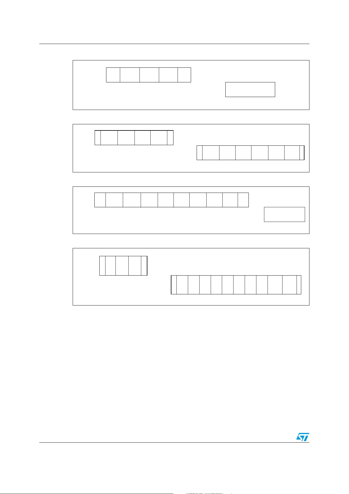
SRI4K command summary SRI4K
SOF 0Ch CRCLCRCHEOF
AI10889
Reader
SRI4K
No Response
S
O
F
Data 1
AI10890c
Data 2 Data 3 Data 4
Reader
SRI4K
CRCLCRC
H
E
O
F
<-t0-><-t1->
S
O
F
08h CRCLCRC
H
E
O
F
Address
Data 1
AI10891b
Data 2 Data 3 Data 4
Reader
SRI4K
CRCLCRCHEOF
SOF 09h
Address
No response
S
O
F
CRCLCRC
H
E
O
F
AI10892b
Reader
SRI4K
<-t0-><-t1->
S
O
F
CRCLCRC
H
E
O
F
0Bh
UID1UID2UID3UID
4
UID
0
UID5UID6UID
7
Figure 57. Reset_to_inventory frame exchange between reader and SRI4K
Figure 58. Read_block frame exchange between reader and SRI4K
Figure 59. Write_block frame exchange between reader and SRI4K
Figure 60. Get_UID frame exchange between reader and SRI4K
44/46 Doc 11605 Rev 5
Page 45

SRI4K Revision history
Revision history
Table 11. Document revision history
Date Version Changes
13-Jan-2005 1.0 First issue
01-Sep-2005 2.0 Updated initial counter values in 32-bit binary counters on page 16.
Document reformatted. Small text changes.
All antennas are ECOPACK® compliant.
min and max values
TUN
10-Apr-2007 3
28-Aug-2008 4
09-Sep-2011 5
Unique identifier (UID) on page 37 added. C
removed, typical value added in Table 8: DC characteristics.
Space removed between t0 and t1 in the “frame exchange between
Reader and SRI4K” Figures (see Appendix B: SRI4K command
summary on page 43.
SRI4K no longer delivered in A3, A4 and A5 antennas.
Table 6: Absolute maximum ratings and Table 10: Ordering information
scheme clarified. Small text changes.
Document converted to new template. Updated disclaimer on last
page.
Process technology removed from Section 1: Description.
Doc 11605 Rev 5 45/46
Page 46

SRI4K
Please Read Carefully:
Information in this document is provided solely in connection with ST products. STMicroelectronics NV and its subsidiaries (“ST”) reserve the
right to make changes, corrections, modifications or improvements, to this document, and the products and services described herein at any
time, without notice.
All ST products are sold pursuant to ST’s terms and conditions of sale.
Purchasers are solely responsible for the choice, selection and use of the ST products and services described herein, and ST assumes no
liability whatsoever relating to the choice, selection or use of the ST products and services described herein.
No license, express or implied, by estoppel or otherwise, to any intellectual property rights is granted under this document. If any part of this
document refers to any third party products or services it shall not be deemed a license grant by ST for the use of such third party products
or services, or any intellectual property contained therein or considered as a warranty covering the use in any manner whatsoever of such
third party products or services or any intellectual property contained therein.
UNLESS OTHERWISE SET FORTH IN ST’S TERMS AND CONDITIONS OF SALE ST DISCLAIMS ANY EXPRESS OR IMPLIED
WARRANTY WITH RESPECT TO THE USE AND/OR SALE OF ST PRODUCTS INCLUDING WITHOUT LIMITATION IMPLIED
WARRANTIES OF MERCHANTABILITY, FITNESS FOR A PARTICULAR PURPOSE (AND THEIR EQUIVALENTS UNDER THE LAWS
OF ANY JURISDICTION), OR INFRINGEMENT OF ANY PATENT, COPYRIGHT OR OTHER INTELLECTUAL PROPERTY RIGHT.
UNLESS EXPRESSLY APPROVED IN WRITING BY TWO AUTHORIZED ST REPRESENTATIVES, ST PRODUCTS ARE NOT
RECOMMENDED, AUTHORIZED OR WARRANTED FOR USE IN MILITARY, AIR CRAFT, SPACE, LIFE SAVING, OR LIFE SUSTAINING
APPLICATIONS, NOR IN PRODUCTS OR SYSTEMS WHERE FAILURE OR MALFUNCTION MAY RESULT IN PERSONAL INJURY,
DEATH, OR SEVERE PROPERTY OR ENVIRONMENTAL DAMAGE. ST PRODUCTS WHICH ARE NOT SPECIFIED AS "AUTOMOTIVE
GRADE" MAY ONLY BE USED IN AUTOMOTIVE APPLICATIONS AT USER’S OWN RISK.
Resale of ST products with provisions different from the statements and/or technical features set forth in this document shall immediately void
any warranty granted by ST for the ST product or service described herein and shall not create or extend in any manner whatsoever, any
liability of ST.
ST and the ST logo are trademarks or registered trademarks of ST in various countries.
Information in this document supersedes and replaces all information previously supplied.
The ST logo is a registered trademark of STMicroelectronics. All other names are the property of their respective owners.
© 2011 STMicroelectronics - All rights reserved
STMicroelectronics group of companies
Australia - Belgium - Brazil - Canada - China - Czech Republic - Finland - France - Germany - Hong Kong - India - Israel - Italy - Japan -
Malaysia - Malta - Morocco - Philippines - Singapore - Spain - Sweden - Switzerland - United Kingdom - United States of America
www.st.com
46/46 Doc 11605 Rev 5
 Loading...