

Page 1
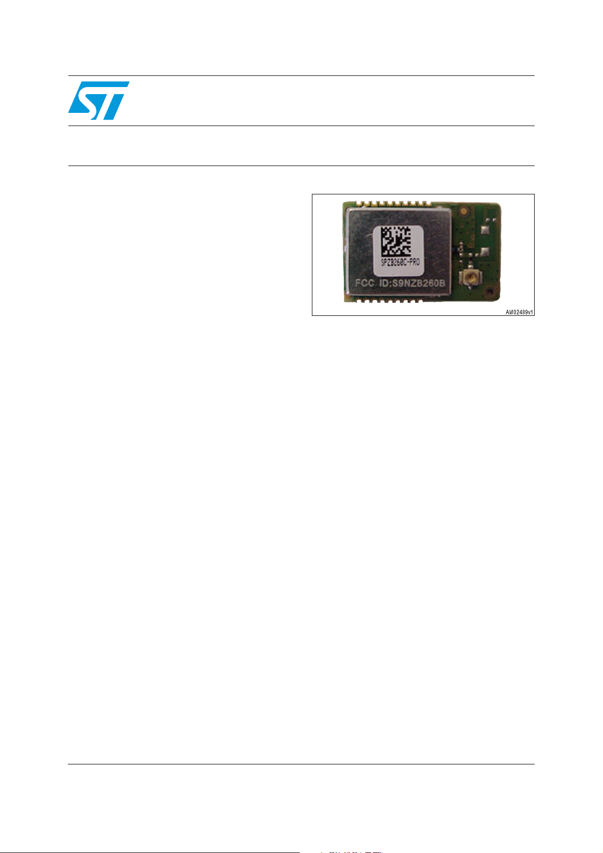
Low-power, compact ZigBee® module
Features
■ Integrated 2.4 GHz, IEEE 802.15.4 compliant
transceiver:
– + 3 dBm nominal TX output power (at UFL
connector level)
– + 5 dBm in boost mode
– -95 dBm (typ) RX sensitivity
– RX filtering for co-existence with IEEE
802.11g and Bluetooth
– Integrated VCP and loop filter
■ SPI or UART interface available for connection
with a host processor
■ On-board 24 MHz stable Xtal
■ Operates in the -40 °C to +85 °C industrial
temperature range
■ 1 µA power consumption in deep sleep mode
■ Pins available for non-intrusive debug interface
(SIF)
■ Single supply voltage (2.1 V to 3.6 V)
■ Integrated RF UFL connector for external
antenna
■ CE and RoHS compliant
■ FCC compliant (FCC ID: S9NZB260B)
®
devices
SPZB260C-PRO
Description
The SPZB260C-PRO is a low power, compact
ZigBee
applications. It enables OEMs to easily add
wireless capability to electronic devices.
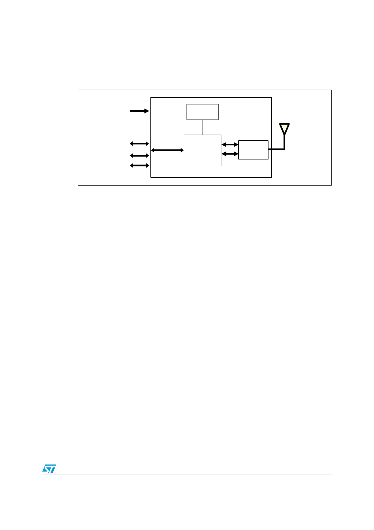
The module is based on the EM260 ZigBee
network processor, which integrates a 2.4 GHz
IEEE 802.15.4 compliant transceiver and IEEE
802.15.4 PHY and MAC.
A single supply voltage is required to power the
module. The voltage supply also determines the
I/O port level, allowing easy integration with the
target device. The module integrates an RF UFL
connector, allowing the use of an external
antenna.
®
module optimized for embedded
Applications
The EM260 provides an SPI-based serial
interface (EZSP - EmberZNet serial protocol) or
■ Industrial control
■ Sensor networking
■ Monitoring of remote systems
■ Home appliances
■ Security systems
■ Lighting control
■ Metering
September 2010 Doc ID 17301 Rev 1 1/15
UART interface to the EmberZNet APIs, both
accessible from the module.
The module is shipped with the EmberZnet PRO
version 3.3.1 loaded into the Flash memory for
use of the SPI-based serial interface.
For details or additional information, please refer
to the EM260 datasheet available on the Ember
Corporation website.
www.st.com
15
Page 2

Contents SPZB260C-PRO
Contents
1 Block diagram . . . . . . . . . . . . . . . . . . . . . . . . . . . . . . . . . . . . . . . . . . . . . . 3
2 Pin information . . . . . . . . . . . . . . . . . . . . . . . . . . . . . . . . . . . . . . . . . . . . . 4
2.1 Pin connections . . . . . . . . . . . . . . . . . . . . . . . . . . . . . . . . . . . . . . . . . . . . . 4
2.2 Pin description . . . . . . . . . . . . . . . . . . . . . . . . . . . . . . . . . . . . . . . . . . . . . . 5
3 Maximum ratings . . . . . . . . . . . . . . . . . . . . . . . . . . . . . . . . . . . . . . . . . . . . 6
3.1 Absolute maximum ratings . . . . . . . . . . . . . . . . . . . . . . . . . . . . . . . . . . . . . 6
3.2 Operating ranges . . . . . . . . . . . . . . . . . . . . . . . . . . . . . . . . . . . . . . . . . . . . 6
4 Electrical characteristics . . . . . . . . . . . . . . . . . . . . . . . . . . . . . . . . . . . . . 7
4.1 DC electrical characteristics . . . . . . . . . . . . . . . . . . . . . . . . . . . . . . . . . . . . 7
4.2 DC I/O specifications . . . . . . . . . . . . . . . . . . . . . . . . . . . . . . . . . . . . . . . . . 7
4.3 RF electrical characteristics . . . . . . . . . . . . . . . . . . . . . . . . . . . . . . . . . . . . 8
5 Package mechanical dimensions . . . . . . . . . . . . . . . . . . . . . . . . . . . . . . 9
6 Soldering . . . . . . . . . . . . . . . . . . . . . . . . . . . . . . . . . . . . . . . . . . . . . . . . . 11
Appendix A FCC statement . . . . . . . . . . . . . . . . . . . . . . . . . . . . . . . . . . . . . . . . . . 12
A.1 Instructions for FCC ID labeling . . . . . . . . . . . . . . . . . . . . . . . . . . . . . . . . 12
A.2 Special requirement for modular application. . . . . . . . . . . . . . . . . . . . . . . 13
Revision history . . . . . . . . . . . . . . . . . . . . . . . . . . . . . . . . . . . . . . . . . . . . . . . . . . . . 14
2/15 Doc ID 17301 Rev 1
Page 3
SPZB260C-PRO Block diagram
1 Block diagram
Figure 1. SPZB260C-PRO block diagram
6
$$
3)&
30)<5!24
#/.423)'.
-(Z
84!,
%-
4RANSCEIVER
2&
ANTENNA
"ALUN
&ILTER
!-V
Doc ID 17301 Rev 1 3/15
Page 4

Pin information SPZB260C-PRO
2 Pin information
2.1 Pin connections
Figure 2. Pin connection diagram
4/15 Doc ID 17301 Rev 1
Page 5
SPZB260C-PRO Pin information
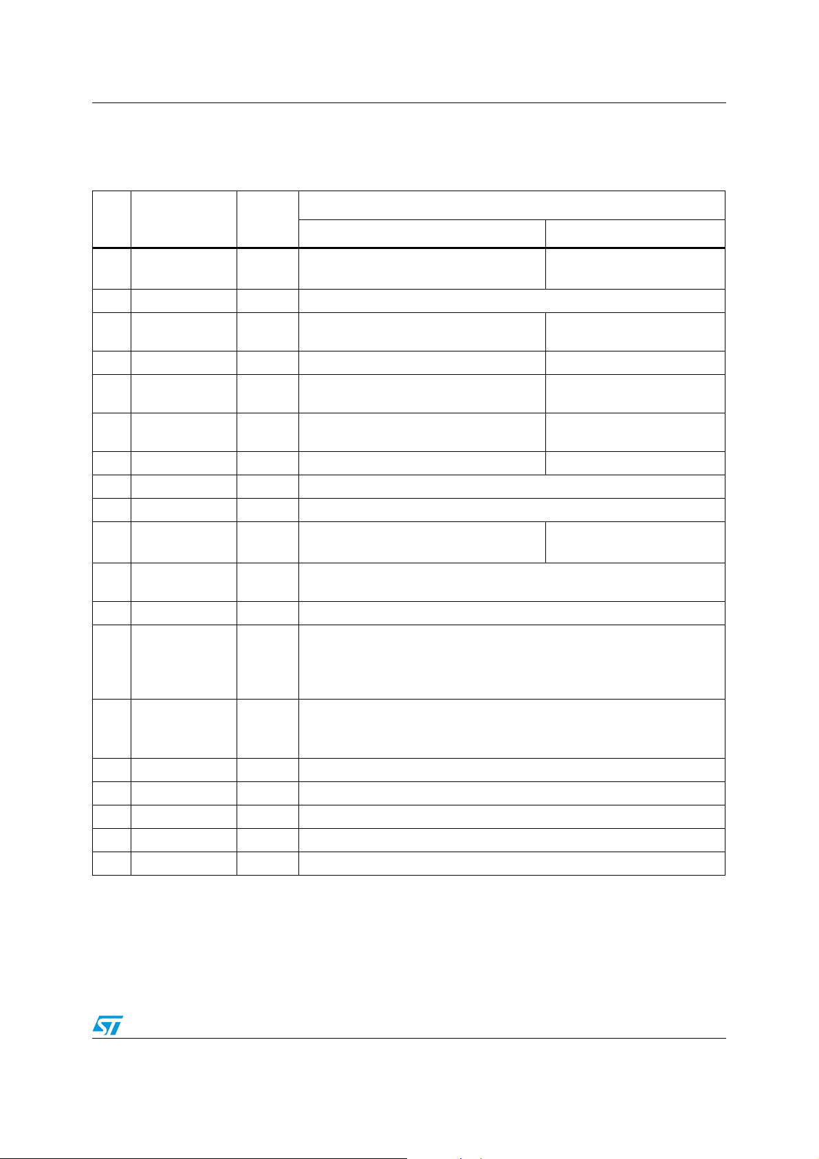
2.2 Pin description
Table 1. Pin description
Description
Pin n Pin name Direction
SPI mode UART mode
1 RTS O Not used
RTS signal
(10 kΩ pull-up to VDD)
2 RSTB I Active low reset (a pull-up of 10 kΩ typ is provided with 10 nF to GND)
3 HOST_INT / RXD O /I
Host interrupt signal (from ZB module to
host) - SPI mode
RXD signal
4 SPI_SSEL / CTS I SPI slave select (from host to ZB module) CTS signal
5 SPI MOSI I
6 SPI MISO O
SPI data, master out/slave in (from host to
ZB module)
SPI data, master in/slave out (from ZB
module to host)
Not used
Not used
7 SPI_CLK I SPI clock Not used
8 GND --- Ground
9
10 TXD O Not used
11 SIF_CLK I
VDD --- Input power supply
TXD signal
(10 kΩ pull-up to VDD)
Non-intrusive debug interface. Serial interface clock signal (internal pulldown)
12 SIF_MISO O Non-intrusive debug interface. Serial interface master in/slave out
Non-intrusive debug interface
13 SIF_MOSI I
Serial interface master out/slave in
To guarantee proper signal level when in deep sleep mode, a 10 kΩ resistor
to GND is included
Non-intrusive debug Interface
14 SIF_LOADB I/O
Serial interface load strobe (open collector with internal pull-up).
To improve noise immunity, a 10 kΩ resistor to Vdd is included
15 PTI_EN O Frame signal of packet trace interface (PTI)
16 PTI_DATA O Data signal of packet trace interface (PTI)
17 WAKE I Wake interrupt signal from host to ZB module
18 ACTIVITY O Activity signal for application debug /monitor
19 SDBG O Spare debug signal
Doc ID 17301 Rev 1 5/15
Page 6
Maximum ratings SPZB260C-PRO
3 Maximum ratings
3.1 Absolute maximum ratings
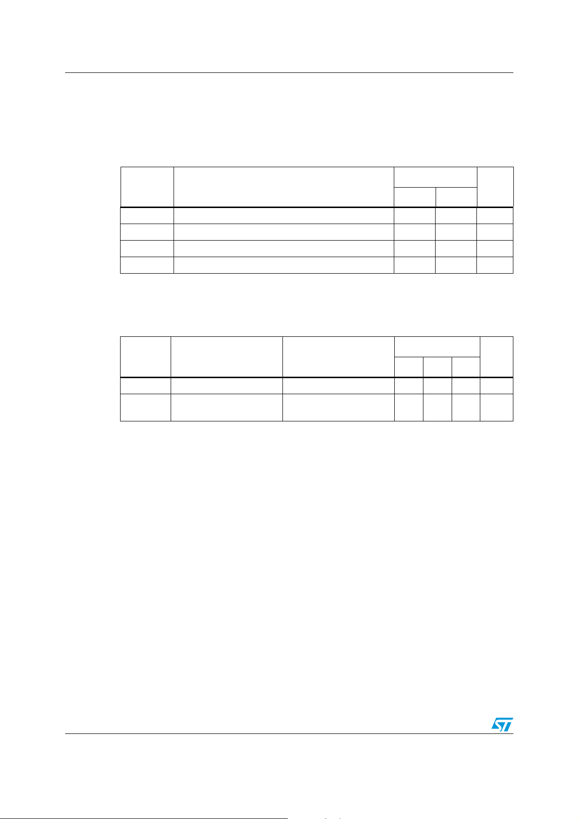
Table 2. Absolute maximum ratings
Values
Symbol Parameter
Min. Max.
Unit
V
DD
V
IN
T
stg
T
sold
Module supply voltage -0.3 3.6 V
Input voltage on any digital pin -0.3 Vdd+0.3 V
Storage temperature -40 +85 °C
Soldering temperature < 10 s 250 °C
3.2 Operating ranges
Table 3. Operating ranges
Symbol Parameter Conditions
V
DD
T
stg
Module supply voltage - 40 °C < T < 85 °C 2.1 3.3 3.6 V
Operating ambient
temperature
Val ues
Unit
Min. Typ. Max.
-40 +85 °C
6/15 Doc ID 17301 Rev 1
Page 7
SPZB260C-PRO Electrical characteristics
4 Electrical characteristics
4.1 DC electrical characteristics
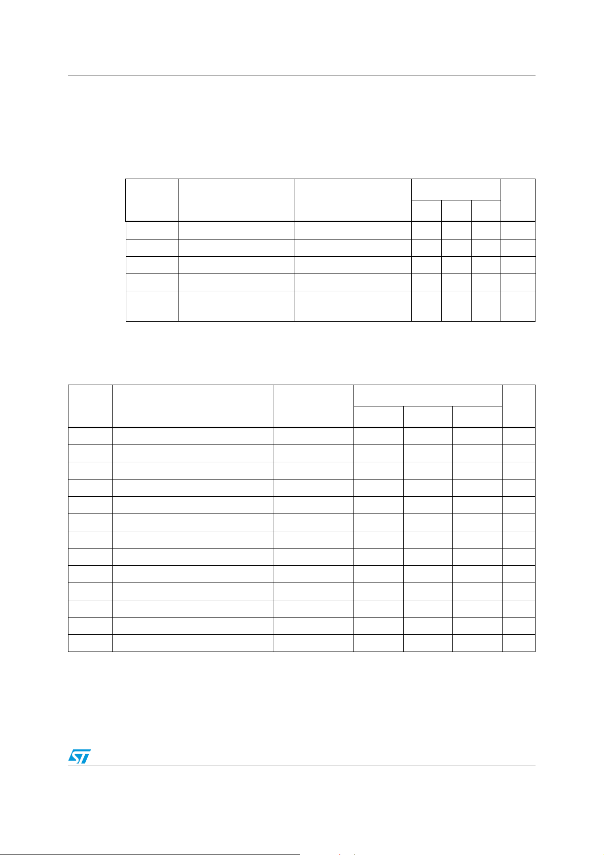
Table 4. DC electrical characteristics
Val ues
Symbol Parameter Conditions
IRX RX current (boost mode) Vdd = 3.0 V, T = 25 °C - 38 mA
IRX RX current (normal mode) Vdd = 3.0 V, T = 25 °C - 36 mA
ITX TX current (boost mode) Vdd = 3.0 V, T = 25 °C - 42 mA
ITX TX current (normal mode) Vdd = 3.0 V, T = 25 °C - 36 mA
IDS Deep sleep current
4.2 DC I/O specifications
2.1 < Vdd < 3.6 V
T = 25°C
Min. Typ. Max.
-1μA
Unit
Table 5. DC input/output specifications
Symbol Parameter Conditions
VIL Low level input voltage 2.1 < Vdd < 3.6 V 0 0.2 x Vdd V
VIH High level input voltage 2.1 < Vdd < 3.6 V 0.8 x Vdd Vdd V
Iil Input current for logic 0 2.1 < Vdd < 3.6 V -0.5 mA
Iih Input current for logic 1 2.1 < Vdd < 3.6 V 0.5 mA
Ripu Input pull-up resistor 30 kΩ
Ripd Input pull-down resistor 30 kΩ
VOL Low level output voltage 0 0.18 x Vdd V
VOH High level output voltage 0.82 x Vdd Vdd V
IOHS Output source current 4 mA
IOLS Output sink current 4 mA
IOHH Output source current (pin 15,16,17) 8 mA
IOLH Output sink current (pin 15,16,17) 8 mA
IOTot Total output current for I/O 40 mA
Val ues
Unit
Min. Typ. Max.
Doc ID 17301 Rev 1 7/15
Page 8

Electrical characteristics SPZB260C-PRO
4.3 RF electrical characteristics
Table 6. RF electrical characteristics
Val ues
Symbol Parameter Conditions
Min. Typ. Max.
Frequency range 2.1 < Vdd < 3.6 V 2405 2480 MHz
TX Output power Vdd = 3.0 V, F = 2450 MHz 3 dBm
RX Sensitivity Vdd = 3.0 V, 1% PER -95 dBm
CFE Carrier frequency error Vdd = 3.0 V -20 / + 70 °C -40 40 ppm
Unit
8/15 Doc ID 17301 Rev 1
Page 9
SPZB260C-PRO Package mechanical dimensions
5 Package mechanical dimensions
In order to meet environmental requirements, ST offers these devices in different grades of
ECOPACK
specifications, grade definitions and product status are available at: www.st.com.
ECOPACK
®
packages, depending on their level of environmental compliance. ECOPACK®
®
is an ST trademark.
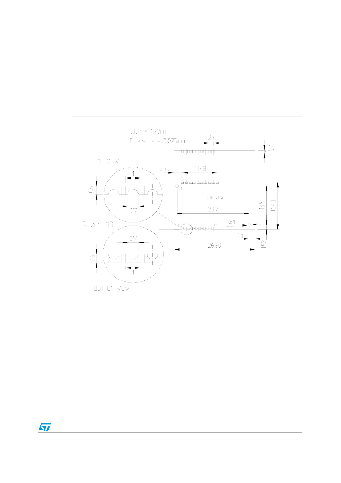
Figure 3. Mechanical dimensions
Doc ID 17301 Rev 1 9/15
Page 10
Package mechanical dimensions SPZB260C-PRO
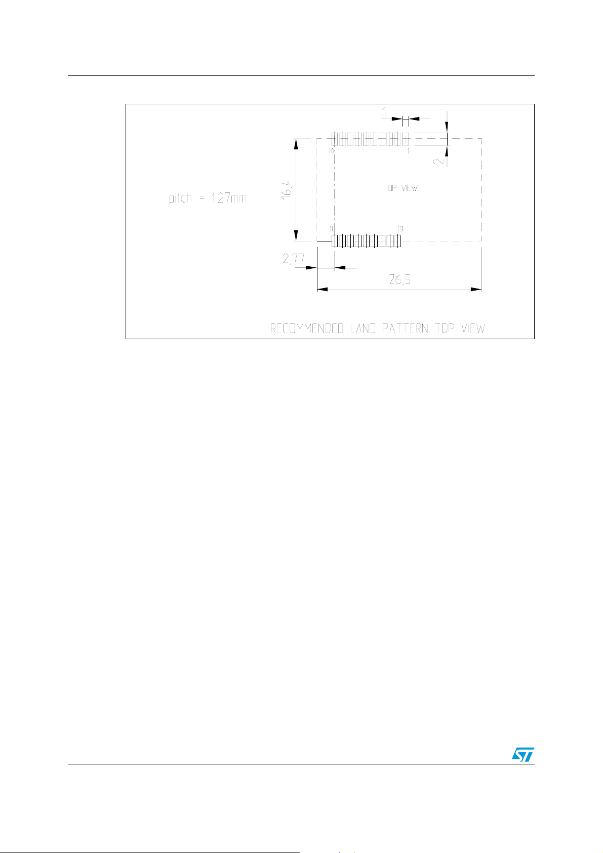
Figure 4. Solder pad layout
10/15 Doc ID 17301 Rev 1
Page 11
SPZB260C-PRO Soldering
6 Soldering
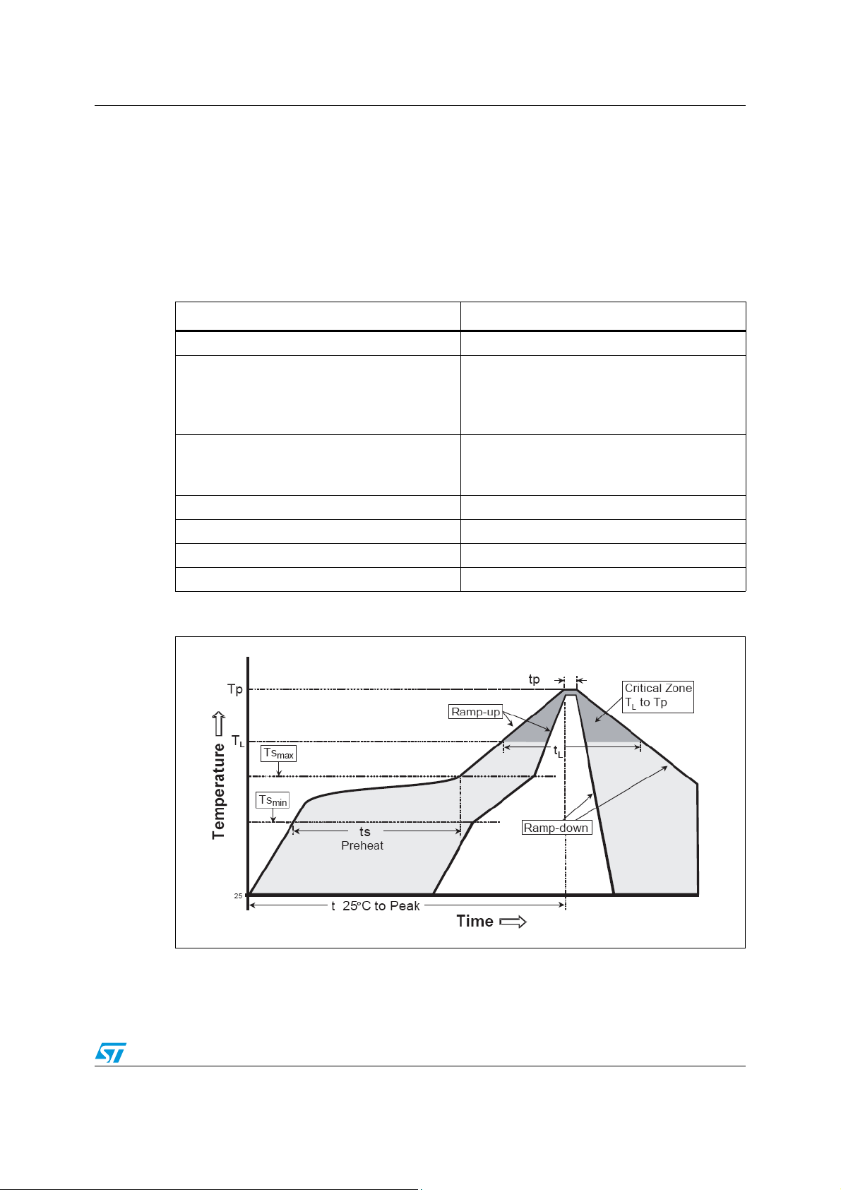
Care should be taken during the soldering phase to avoid undesired melting, with particular
attention on the peak temperature setting.
The following are some suggestions for the temperature profile based on IPC/JEDEC JSTD-020C, July 2004 recommendations.
Table 7. Soldering profile
Profile feature PB free assembly
Average ramp up rate (T
SMAX to TP) 3 °C / sec max
Preheating:
Temperature min. (T
S MIN)
Temperature max. (TS MAX)
Time (T
S MIN to TS MAX) (tS)
150 °C
200 °C
60 – 100 sec
Time maintained above:
Temperature T
Time tL
L
217 °C
40 – 70 sec
Peak temperature (Tp) 240+0 °C
Time within 5 °C of actual peak temperature (t
P) 10 – 20 sec
Ramp down rate 6 °C / sec
Time from 25 °C to peak temperature 8 minutes max
Figure 5. Soldering
Doc ID 17301 Rev 1 11/15
Page 12

FCC statement SPZB260C-PRO
Appendix A FCC statement
This device complies with part 15 of the FCC rules. Operation is subject to the following two
conditions: (1) this device may not cause harmful interference, and (2) this device must
accept any interference received, including interference that may cause undesired
operation.
Note: This equipment has been tested and found to comply with the limits for a class B digital
device, pursuant to part 15 of the FCC rules. These limits are designed to provide
reasonable protection against harmful interference in a residential installation. This
equipment generates, uses and can radiate radio frequency energy and, if not installed and
used in accordance with the instructions, may cause harmful interference to radio
communications. However, there is no guarantee that interference will not occur in a
particular installation. If this equipment does cause harmful interference to radio or
television reception, which can be determined by turning the equipment off and on, the user
is encouraged to try to correct the interference by one or more of the following measures:
● Reorient or relocate the receiving antenna
● Increase the separation between the equipment and receiver
● Connect the equipment to an outlet on a circuit different from which the receiver is
connected
Consult the dealer or an experienced radio/TV technician for assistance.
Antenna
Module type SPZB260 is for OEM integration only. The end-user product must be
professionally installed in such a manner that only the authorized antennas are used.
Caution: Changes or modifications not expressly approved by the party responsible for compliance
may cause the module to cease to comply with part 15 of the FCC rules, thus voiding the
user’s authorization to operate the equipment.
A.1 Instructions for FCC ID labeling
Module type: ZigBee® module SPZB260C-PRO
FCC-ID: S9NZB260B
This is intended as a guideline for specifying the FCC ID of the ZigBee
SPZB260C-PRO on the end product.
Based on the public notice from the FCC, the product into which this transmitter module is
installed must display a label referring to the module.
The label should consist of wording such as “contains transmitter module FCC ID:
S9NZB260B” or “contains FCC ID: S9NZB260B”, or any similar wording which conveys the
same meaning.
For example:
Contains FCC ID:
S9NZB260B
®
module
12/15 Doc ID 17301 Rev 1
Page 13

SPZB260C-PRO FCC statement
A.2 Special requirement for modular application
The following requirements are fulfilled:
1. The modular transmitter must have its own RF shielding:
The RF module used on the board fulfils the emission requirements of the relevant
FCC rules without additional shielding.
2. The modular transmitter must have buffered modulation/data inputs:
The module has a memory management unit integrated in the IC. The processor
interfaces with the external application by means of general purpose I/O (GPIO), UART
or SPI. The processor also interfaces with the RF part of the module, exchanging data
and commands with it. Inside the processor, Flash memory is available to download the
customer application and the ZigBee
3. The modular transmitter must have its own power supply regulation:
The IC contains a voltage regulation function. In case of changes in the supply voltage
V
(due to temperature changes, for example), the internal voltage is stabilized.
CC
4. The modular transmitter must comply with the antenna requirements of section 15.203
and 15.204:
The RF module is for OEM (original equipment manufacturer) integration only. The enduser product must be professionally installed in such a manner that only the authorized
antenna is used.
5. The modular transmitter must be tested in a stand-alone configuration:
The RF module was tested in a stand-alone configuration.
6. The modular transmitter must be labelled with its own FCC ID number:
The RF module must be labeled with its own FCC ID number. When the module is
installed in the end-product, this label is not visible. The OEM manufacturer is
instructed on how to apply an exterior label.
7. The modular transmitter must comply with any specific rules or operating requirements
applicable to the transmitter, and the manufacturer must provide adequate instructions
along with the module to explain any such requirements:
The EUT is compliant with all applicable FCC rules. Detailed instructions are provided
in the product’s user guide.
8. The modular transmitter must comply with any applicable RF exposure requirements.
– Maximum measured power output: 3.17 mW
– Maximum antenna gain: 2.2 dBi = numeric gain 1.66 (also see FCC test report)
®
profiles.
Maximum permissible exposure defined in 47 CFR 1.1310: 1 mW/cm².
The RF module operates at a low power level which does not exceed the commission’s RF
exposure guideline limits. Moreover, spread spectrum transmitters operating according to
section 15.247 are categorically excluded from routine environmental evaluation.
Doc ID 17301 Rev 1 13/15
Page 14

Revision history SPZB260C-PRO
Revision history
Table 8. Document revision history
Date Revision Changes
09-Sep-2010 1 First release.
14/15 Doc ID 17301 Rev 1
Page 15

SPZB260C-PRO
Please Read Carefully:
Information in this document is provided solely in connection with ST products. STMicroelectronics NV and its subsidiaries (“ST”) reserve the
right to make changes, corrections, modifications or improvements, to this document, and the products and services described herein at any
time, without notice.
All ST products are sold pursuant to ST’s terms and conditions of sale.
Purchasers are solely responsible for the choice, selection and use of the ST products and services described herein, and ST assumes no
liability whatsoever relating to the choice, selection or use of the ST products and services described herein.
No license, express or implied, by estoppel or otherwise, to any intellectual property rights is granted under this document. If any part of this
document refers to any third party products or services it shall not be deemed a license grant by ST for the use of such third party products
or services, or any intellectual property contained therein or considered as a warranty covering the use in any manner whatsoever of such
third party products or services or any intellectual property contained therein.
UNLESS OTHERWISE SET FORTH IN ST’S TERMS AND CONDITIONS OF SALE ST DISCLAIMS ANY EXPRESS OR IMPLIED
WARRANTY WITH RESPECT TO THE USE AND/OR SALE OF ST PRODUCTS INCLUDING WITHOUT LIMITATION IMPLIED
WARRANTIES OF MERCHANTABILITY, FITNESS FOR A PARTICULAR PURPOSE (AND THEIR EQUIVALENTS UNDER THE LAWS
OF ANY JURISDICTION), OR INFRINGEMENT OF ANY PATENT, COPYRIGHT OR OTHER INTELLECTUAL PROPERTY RIGHT.
UNLESS EXPRESSLY APPROVED IN WRITING BY AN AUTHORIZED ST REPRESENTATIVE, ST PRODUCTS ARE NOT
RECOMMENDED, AUTHORIZED OR WARRANTED FOR USE IN MILITARY, AIR CRAFT, SPACE, LIFE SAVING, OR LIFE SUSTAINING
APPLICATIONS, NOR IN PRODUCTS OR SYSTEMS WHERE FAILURE OR MALFUNCTION MAY RESULT IN PERSONAL INJURY,
DEATH, OR SEVERE PROPERTY OR ENVIRONMENTAL DAMAGE. ST PRODUCTS WHICH ARE NOT SPECIFIED AS "AUTOMOTIVE
GRADE" MAY ONLY BE USED IN AUTOMOTIVE APPLICATIONS AT USER’S OWN RISK.
Resale of ST products with provisions different from the statements and/or technical features set forth in this document shall immediately void
any warranty granted by ST for the ST product or service described herein and shall not create or extend in any manner whatsoever, any
liability of ST.
ST and the ST logo are trademarks or registered trademarks of ST in various countries.
Information in this document supersedes and replaces all information previously supplied.
The ST logo is a registered trademark of STMicroelectronics. All other names are the property of their respective owners.
© 2010 STMicroelectronics - All rights reserved
Australia - Belgium - Brazil - Canada - China - Czech Republic - Finland - France - Germany - Hong Kong - India - Israel - Italy - Japan -
STMicroelectronics group of companies
Malaysia - Malta - Morocco - Philippines - Singapore - Spain - Sweden - Switzerland - United Kingdom - United States of America
www.st.com
Doc ID 17301 Rev 1 15/15
 Loading...