

Page 1
FEATURES
SPT9689
DUAL ULTRAFAST VOLT AGE COMPARATOR
TECHNICAL DATA
FEBRUARY 20, 2001
APPLICATIONS
• 650 ps propagation delay
• 100 ps propagation delay variation
• 70 dB CMRR
• Low feedthrough and crosstalk
• Differential latch control
• ECL compatible
GENERAL DESCRIPTION
The SPT9689 is a
parator. The propagation delay variation is less than
100 ps from 5 to 50 mV input overdrive v oltage. The input
slew rate is 10 V/ns. The device utilizes a high precision
differential input stage with a common-mode range of
–2.5 V to +4.0 V.
Sub
nanosecond monolithic dual com-
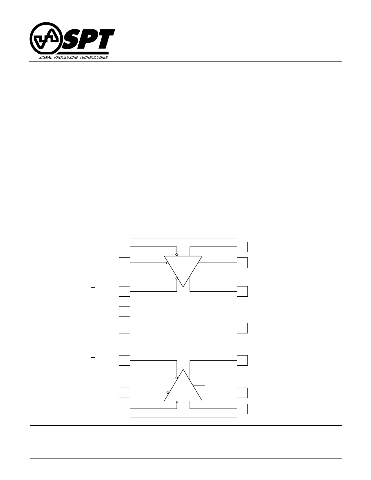
BLOCK DIAGRAM
INVERTING
INPUT
LATCH ENABLE
+
• Automated test equipment
• High-speed instrumentation
• Window comparators
• High-speed timing
• Line receivers
• High-speed triggers
• Threshold detection
• Peak detection
ECL-compatible complementary digital outputs are capable of driving 50 Ω terminated transmission lines and
providing 30 mA output drive. The SPT9689 is pin compatible with the SPT9687. It is a v ailable in 20-lead PLCC and
20-contact LCC packages over the industrial temperature
range. The SPT9689 is also available in die form.
NONINVERTING
INPUT
A
LATCH ENABLE
Q OUTPUT
V
V
GND
Q OUTPUT
LATCH ENABLE
INVERTING
INPUT
CC
EE
A
B
+
Q OUTPUT
GND
B
Q OUTPUT
LATCH ENABLE
NONINVERTING
INPUT
Signal Processing Technologies, Inc.
4755 Forge Road, Colorado Springs, Colorado 80907, USA
Phone: 719-528-2300 Fax: 719-528-2370 Web Site: http://www .spt.com e-mail: sales@spt.com
Page 2
ABSOLUTE MAXIMUM RATINGS (Beyond which damage may occur)1 25 °C
Supply Voltages
Positive Supply Voltage (VCC to GND).... –0.5 to +6.0 V
Negative Supply Voltage (VEE to GND) ..–6.0 to +0.5 V
Ground V oltage Differential ....................–0.5 to +0.5 V
Input Voltages
Input Common Mode Voltage .................–4.0 to +5.0 V
Differential Input Voltage ........................ –3.0 to +3.0 V
Input Voltage, Latch Controls ....................V
to 0.5 V
EE
Output
Output Current ................................................... 30 mA
Temperature
Operating Temperature, ambient............ –40 to +85 °C
junction ..................... +150 °C
Lead Temperature, (soldering 60 seconds) ..... +300 °C
Storage Temperature............................ –65 to +150 °C
Note: 1. Operation at any Absolute Maximum Rating is not implied. See
Electrical Specifications for proper nominal applied conditions
in typical applications.
ELECTRICAL SPECIFICATIONS
T A = +25 °C, VCC = +5.0 V, VEE =–5.20 V , RL = 50 Ohm to –2 V, unless otherwise specified.
PARAMETERS CONDITIONS LEVEL MIN TYP MAX MIN TYP MAX UNITS
DC CHARACTERISTICS
Input Offset Voltage V
Input Offset Voltage V
Offset Voltage Tempco V 10 40 µV/°C
Input Bias Current I ±8 ±25 ±8 ±25 µA
Input Bias Current T
Input Offset Current I ±1.0 ±3.0 ±2.0 ±5.0 µA
Input Offset Current T
Positive Supply Current Dual I 18 30 18 35 mA
Negative Supply Current Dual I 40 55 40 60 mA
Positiv e Supply Voltage, V
Negative Supply Voltage, V
Input Common Mode Range V –2.5 +4.0 –2.5 +4.0 V
Latch Enable
Common Mode Range IV –2.0 0 –2.0 0 V
Open Loop Gain V 66 66 dB
Differential Input Resistance V 500 500 kΩ
Input Capacitance V 0.6 0.6 pF
Power Supply Sensitivity V 70 70 dB
Common Mode Rejection Ratio VCM=–2.5 to +4.0 V 70 70 dB
Power Dissipation Dual, Without Load I 350 425 350 4 75 mW
Power Dissipation Dual, With Load I 400 550 400 550 mW
Output High Level ECL 50 Ohms to –2 V I –1.00 –.81 –1.00 –.81 V
Output Low Level ECL 50 Ohms to –2 V I –1.95 –1.54 –1.95 –1.54 V
CC
TEST TEST SPT9689A SPT9689B
1
1
I –10 ±3.0 10 –25 ±12 25 mV
IV –15 ±4.5 15 –30 ±15 30 mV
IV ±12 ±38 ±12 ±38 µA
IV ±2.0 ±5.0 ±4.0 ±7.0 µA
IV 4.75 5.0 5.25 4.75 5.0 5.25 V
IV –4.95 –5.2 –5.45 –4.95 –5.2 –5.45 V
EE
=0, RS=0 Ohms
IN, CM
=0, RS=0 Ohms
IN, CM
T
MIN<TA<TMAX
MIN<TA<TMAX
MIN<TA<TMAX
AC CHARACTERISTICS
Propagation Delay 20 mV O.D. IV 650 850 750 950 ps
Latch Set-up Time V 150 300 150 300 ps
Latch to Output Delay 250 mV O.D. V 500 600 500 600 ps
Latch Pulse Width V 500 500 ps
Latch Hold Time V 0 0 ps
Rise Time 20% to 80% V 180 180 ps
Fall Time 20% to 80% V 80 80 ps
Slew Rate V 10 10 V/ns
Bandwidth –3 dB V 900 900 M Hz
1
RS = Source impedance
SPT9689
SPT
2 2/20/01
Page 3
TEST LEVEL CODES
All electrical characteristics are subject to the
following conditions:
All parameters having min/max specifications
are guaranteed. The Test Level column indicates the specific device testing actually performed during production and Quality Assurance inspection. Any blank section in the data
column indicates that the specification is not
tested at the specified condition.
LEVEL TEST PROCEDURE
I 100% production tested at the specified temperature.
II 100% production tested at T
specified temperatures.
III QA sample tested only at the specified temperatures.
IV Parameter is guaranteed (but not tested) by design and characteri-
zation data.
V Parameter is a typical value for information purposes only.
VI 100% production tested at TA = +25 °C. Parameter is guaranteed
over specified temperature range.
= +25 °C, and sample tested at the
A
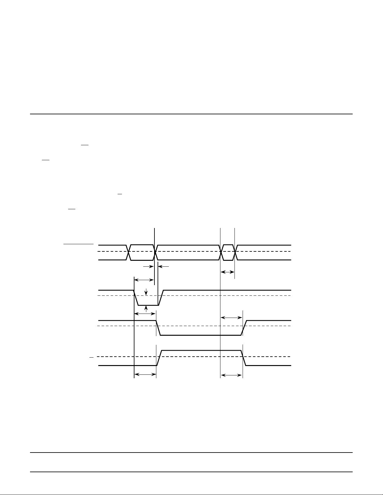
TIMING INFORMATION
The timing diagram for the comparator is shown in figure
1. If LE is high and LE low in the SPT9689, the compar ator
tracks the input difference voltage. When LE is driven low
and LE high, the comparator outputs are latched into their
existing logic states.
The leading edge of the input signal (which consists of a
20 mV overdrive voltage) changes the comparator output
after a time of t
be maintained for a time tS (set-up time) before the LE falling edge and LE rising edge and held for time tH after the
Figure 1 – Timing Diagram
or t
pdL
Latch Enable
Latch Enable
Differential
Input Voltage
Output Q
(Q or Q). The input signal must
pdH
t
H
t
S
V
OD
t
pdL
falling edge for the compar ator to accept data. After tH, the
output ignores the input status until the latch is strobed
again. A minimum latch pulse width of tpL is needed for
strobe operation, and the output transitions occur after a
time of t
pLOH
or t
pLOL
.
The set-up and hold times are a measure of the time
required for an input signal to propagate through the first
stage of the comparator to reach the latching circuitry.
Input signals occurring before tS will be detected and held;
those occurring after tH will not be detected. Changes
between tS and tH may not be detected.
50%
t
pL
V
± V
REF
OS
t
pLOH
50%
SPT
Output Q
t
pdH
VIN+=100 mV (p-p), VOD=20 mV
3 2/20/01
t
pLOL
50%
SPT9689
Page 4

SWITCHING TERMS (Refer to figure 1)
CC
INPUT TO OUTPUT HIGH DELAY – the propaga-
t
pdH
tion delay measured from the time the input signal
crosses the reference (± the input offset voltage) to
the 50% point of an output LOW to HIGH transition
t
INPUT T O OUTPUT LO W DELAY – the propagation
pdL
delay measured from the time the input signal
crosses the reference (± the input offset voltage) to
the 50% point of an output HIGH to LOW transition
t
LATCH ENABLE TO OUTPUT HIGH DELAY – the
pLOH
propagation delay measured from the 50% point of
the Latch Enable signal LOW to HIGH transition to
the 50% point of an output LOW to HIGH transition
VODVOLTAGE OVERDRIVE – the difference between
the differential input and reference input voltages
GENERAL INFORMATION
LATCH ENABLE TO OUTPUT LOW DELAY – the
t
pLOL
propagation delay measured from the 50% point of
the Latch Enable signal LOW to HIGH transition to
the 50% point of an output HIGH to LOW transition
t
MINIMUM HOLD TIME – the minimum time after the
H
negative transition of the Latch Enable signal that
the input signal must remain unchanged in order to
be acquired and held at the outputs
t
MINIMUM LATCH ENABLE PULSE WIDTH – the
pL
minimum time that the Latch Enable signal must be
HIGH in order to acquire an input signal change
t
MINIMUM SET-UP TIME – the minimum time before
S
the negative transition of the Latch Enable signal
that an input signal change must be present in order
to be acquired and held at the outputs
The SPT9689 is an ultrahigh-speed dual voltage comparator. It offers tight absolute characteristics. The device
has differential analog inputs and complementary logic
outputs compatible with ECL systems. The output stage is
adequate for driving terminated 50 ohm transmission
lines.
The SPT9689 has a complementary latch enable control
for each comparator. Both should be dr iven by standard
ECL logic levels.
Figure 2 – Internal Function Diagram
V
IN
V
IN
REF
1
+
PRE
AMP
REF
2
LATCH
CLK
BUF
The negative common mode voltage is –2.5 V. The positive common mode voltage is +4.0 V.
The dual comparators share the same VCC and VEE connections but have separate grounds for each comparator
to achieve high crosstalk rejection.
Q
ECL
OUT
Q
SPT
V
EE
V
GND
LE LE
SPT9689
4 2/20/01
Page 5

TYPICAL PERFORMANCE CHARACTERISTICS
PROPAGATION DELAY VS OVERDRIVE VOLTAGE
800
RISE AND FALL OF OUTPUTS VS TIME CROSSOVER
.90
750
700
650
600
PROPAGATION DELAY TIME (ps)
550
500
020406080 100
OVERDRIVE (mV)
RISE TIME VS TEMPERATURE
280
240
200
RISE TIME (ps)
160
1.10
1.30
1.50
OUTPUT RISE AND FALL (V)
1.70
1.90
400 500 600 700 800
TIME (ps)
FALL TIME VS TEMPERATURE
260
220
180
FALL TME (ps)
140
900
120
80
11
9
7
5
HYSTERESIS (mV)
3
1
0
-50 0 +50 +100
TEMPERATURE (°C)
+150
HYSTERESIS VS DLATCH
10 20 30 40 50
DLATCH = VLE VLE (mV)
100
60
50 0 +50 +100 +150
TEMPERATURE (°C)
INPUT BIAS CURRENT VS COMMON MODE VOLTAGE
20
16
12
8
INPUT BIAS CURRENT (µA)
4
0
2.0 1.0 0.0 +2.0 +3.0 +4.0 +5.0+1.0
3.0
COMMON MODE VOLTAGE (V)
T=-55 °C
T=+25 °C
T=+125 °C
SPT
SPT9689
5 2/20/01
Page 6

TYPICAL INTERFACE CIRCUIT
The typical interface circuit using the comparator is shown
in figure 3. Although it needs few external components
and is easy to apply, there are several conditions that
should be noted to achieve optimal perf ormance. The v ery
high operating speeds of the comparator require careful
layout, decoupling of supplies , and proper design of transmission lines.
Since the SPT9689 comparator is a very high-frequency
and high-gain device, certain layout rules must be followed to avoid oscillations. The comparator should be
soldered to the board with component lead lengths kept
as short as possible. A g round plane should be used while
the input impedance to the part is kept as low as possible
to decrease parasitic feedback. If the output board traces
are longer than approximately half an inch, microstripline
techniques must be employed to prevent ringing on the
output waveform. Also, the microstriplines must be terminated at the far end with the characteristic impedance of
the line to prevent reflections. Both supply voltage pins
should be decoupled with high-frequency capacitors as
close to the device as possible. All ground pins and no
connects should be soldered to a common ground plane
to further improve noise immunity. If using the SPT9689
as a single comparator, the outputs of the inactive comparator can be grounded, left open, or terminated with
50 ohms to –2 V. All outputs on the active comparator,
whether used or unused, should have identical terminations to minimize ground current switching transients.
Figure 3 – SPT9689 Typical Interface Circuit
+5.0 V
+
+V
V
5.2 V
ECL
CC
LE
LE
GND
EE
R
L
100 pF
10 µF
0.1 µF
50
W
2 V
10 µF
0.1 µF
100 pF
V
IN
V
REF
100 pF
0.1 µF
10 µF
NOTES:
Denotes ground plane.
Ferrite bead. Fair Rite Part # 2643001501.
All resistors are chip type 1%.
0.1 µF and 100 pF capacitors are chip type mounted as close
to the pins as possible.
10 µF tant capacitors have lead lengths <0.25" long.
Represents line termination.
50
R
L
Q Output
Q Output
W
10 F
Figure 4 – SPT9689 Typical Interface Circuit
with Hysteresis
+5.0 V
10 µF
0.1 µF
100 pF
+V
V
IN
V
REF
100 pF
0.1 µF
10 µF
NOTES:
Denotes ground plane.
Ferrite bead. Fair Rite Part # 2643001501.
All resistors are chip type 1%.
0.1 µF and 100 pF capacitors are chip type mounted
as close to the pins as possible.
10 µF tant capacitors have lead lengths <0.25" long.
Represents line termination.
+
CC
V
EE
5.2 V
10 µF
LE
1.3 V
GND
0.1 µF
LE
100 pF
2 V
0 to 200 W
100 W
R
50 W
L
2 V
R
50 W
Q Output
Q Output
L
10 µF
SPT
SPT9689
6 2/20/01
Page 7

PACKAGE OUTLINES
20-Contact Leadless Chip Carrier (LCC)
A
H
INCHES MILLIMETERS
SYMBOL MIN MAX M IN MAX
A .040 typ 1.02 typ
G
B .050 typ 1.27 typ
C 0.045 0.055 1.14 1.40
B
View
Bottom
Pin 1
D 0.345 0.360 8.76 9.14
E 0.054 0.066 1.37 1.68
F .020 typ 0.51 typ
C
D
F
E
G 0.022 0.028 0.56 0.71
H 0.075 1.91
20-Lead Plastic Leadless Chip Carrier (PLCC)
A
G
INCHES MILLIMETERS
B
Pin 1
TOP
VIEW
E
F
N
M
L
SYMBOL MIN MAX M IN MAX
A .045 typ 1.14 typ
B .045 typ 1.14 typ
C 0.350 0.356 8.89 9.04
O
D 0.385 0.395 9.78 10.03
E 0.350 0.356 8.89 9.04
F 0.385 0.395 9.78 10.03
G 0.042 0.056 1.07 1.42
H 0.165 0.180 4.19 4.57
C
D
H
K
J
I
I 0.085 0.110 2.16 2.79
J 0.025 0.040 0.64 1.02
K 0.015 0.025 0.38 0.64
L 0.026 0.032 0.66 0.81
M 0.013 0.021 0.33 0.53
Pin 1
BOTTOM
VIEW
N 0.050 1.27
O 0.290 0.330 7.37 8.38
SPT
SPT9689
7 2/20/01
Page 8

PIN ASSIGNMENTS PIN FUNCTIONS
Q
Q
A
A
N/C
Q
Q
B
B
3 2 1 20 19
GND
4
A
LE
5
A
6
N/C N/C
LE
7
A
V
8
EE
TOP VIEW
18
17
16
15
14
9 10111213
INA+IN
N/C
A
+IN
IN
B
B
LCC/PLCC
GND
LE
B
LE
B
V
CC
B
NAME FUNCTION
Q
A
Q
A
GND
LE
A
LE
A
V
EE
–IN
+IN
+IN
–IN
V
CC
LE
B
LE
B
GND
Q
B
Q
B
A
A
B
B
Output A
Inverted Output A
Ground A
A
Latch Enable A
Inverted Latch Enable A
Negative Supply Voltage
Inverting Input A
Noninverting Input A
Noninverting Input B
Inverting Input B
Positive Supply Voltage
Latch Enabled B
Inverted Latch Enable B
Ground B
B
Output B
Inverted Output B
ORDERING INFORMATION
PART INPUT TEMPERATURE PACKAGE
NUMBER OFFSET RANGE TYPE
SPT9689AIC 10 mV –40 to +85 °C 20C LCC
SPT9689BIC 25 mV –40 to +85 °C 20C LCC
SPT9689AIP 10 mV –40 to +85 °C 20L PLCC
SPT9689BIP 25 mV –40 to +85 °C 20L PLCC
SPT9689ACU +25 °CDie*
SPT9689BCU +25 °CDie*
*Please see the die specification for guaranteed electrical performance.
Signal Processing Technologies, Inc. reserves the right to change products and specifications without notice. Permission is hereby
expressly granted to copy this literature for informational purposes only. Copying this material for any other use is strictly prohibited.
WARNING – LIFE SUPPORT APPLICATIONS POLICY – SPT products should not be used within Life Support Systems without
the specific written consent of SPT. A Life Support System is a product or system intended to support or sustain life which, if it fails,
can be reasonably expected to result in significant personal injury or death.
Signal Processing Technologies believes that ultrasonic cleaning of its products may damage the wire bonding, leading to device
failure. It is therefore not recommended, and exposure of a device to such a process will void the product warranty.
SPT9689
SPT
8 2/20/01
 Loading...