

Page 1
SMALL SIGNAL PNP TRANSISTORS
Type Marking
SO540 1 P33
■ SILICONEPITAXIALPLANAR PNP
TRANSISTORS
■ MINIATUREPLASTIC PACKAGEFOR
APPLICATIONIN SURFACE MOUNTING
CIRCUITS
■ GENERALPURPOSEAND HIGH VOLTAGE
AMPLIFIER
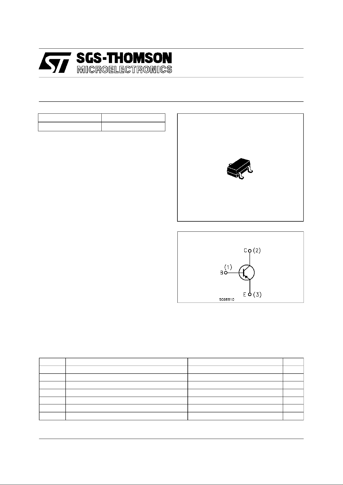
SO5401
2
3
1
SOT-23
INTERNAL SCHEMATIC DIAGRAM
ABSOLUTE MAXIMUM RATINGS
Symb o l Parameter Val u e Uni t
V
V
V
I
P
T
Collect or- B as e V o lt age (IE= 0) -160 V
CBO
Collector-Emitter Voltage (IB= 0) -150 V
CEO
Emitter-Base Voltage (IC=0) -5 V
EBO
Collect or P ea k C ur rent -0. 6 A
CM
Tot al Dis sipation at Tc=25oC 200 mW
tot
Storage Tem perature -65 to 150
stg
Max. Operat ing Junction Temperatu re 150
T
j
o
C
o
C
October 1997
1/4
Page 2
SO5401
THERMAL DATA
R
thj-amb
R
thj-SR
• Mounted on a ceramic substrate area = 7 x 5 x 0.5 mm
Thermal Resistance Junction-Ambient Max
•
•
Ther mal Resistance Junct ion-Subst rate Max
620
400
o
C/W
o
C/W
ELECTRICAL CHARACTERISTICS (T
=25oC unlessotherwise specified)
case
Symbol Parameter Test C ondition s Min. Typ. Max. Unit
I
I
V
(BR) CBO
CBO
EBO
Collector C ut -off
Current (I
E
=0)
Collector C ut -off
Current (I
C
=0)
∗ Collector- E mitter
=-120V -50 nA
V
CB
V
=-3V -50 nA
EB
I
=-100µA-160V
C
Break dow n Voltage
=0)
(I
E
V
∗ Collector- E mitter
(BR) CEO
I
=-1mA -150 V
C
Break dow n Voltage
=0)
(I
B
V
(BR)EBO
Emitt er-Base
I
=-10nA -5 V
C
Break dow n Voltage
=0)
(I
C
V
∗ Collector-Em it t er
CE(sat)
Saturation Voltage
V
∗ Collector-Bas e
BE(sat)
Saturation Voltage
h
∗ DC Curr ent Gain IC=-1mA VCE=-5V
FE
f
C
Tr ansition F requency IC=-10mA VCE= -10V f = 1 MHz 100 400 M Hz
T
Collector Base
CB
IC=-10mA IB=-1mA
=-50mA IB=-5mA
I
C
IC=-10mA IB=-1mA
=-50mA IB=-5mA
I
C
=-10mA VCE=-5V
I
C
=-50mA VCE=-5V
I
C
IE=0 VCE= -10 V f = 1 M H z 6 pF
50
60
50
240
-0.2
-0.5
-1
-1
Capacit a nc e
NF Nois e Fig ure V
∗ Small Signal Curr ent
h
fe
=-5V IC= -0.25 mA f = 1KHz
CE
∆f = 200 Hz R
=1KΩ
G
VCE=-5V IC=-1mA f=1KHz 40 200
5dB
Gain
∗
Pulsed: Pulse duration = 300 µs,duty cycle≤ 2%
V
V
V
V
2/4
Page 3

SOT-23 MECHANICALDATA
S05401
DIM.
MIN. TYP. MAX. MIN. TYP. MAX.
A 0.85 1.1 33.4 43.3
B 0.65 0.95 25.6 37.4
C 1.20 1.4 47.2 55.1
D 2.80 3 110.2 118
E 0.95 1.05 37.4 41.3
F 1.9 2.05 74.8 80.7
G 2.1 2.5 82.6 98.4
H 0.38 0.48 14.9 18.8
L 0.3 0.6 11.8 23.6
M 0 0.1 0 3.9
N 0.3 0.65 11.8 25.6
O 0.09 0.17 3.5 6.7
mm mils
0044616/B
3/4
Page 4

SO5401
Information furnished is believedto be accurate and reliable. However, SGS-THOMSON Microelectronicsassumes no responsability for the
consequencesof use ofsuch information nor for anyinfringement of patentsor other rights of third parties which may resultsfrom its use. No
licenseis grantedby implicationor otherwise underany patent or patentrights of SGS-THOMSON Microelectronics.Specificationsmentioned
in this publication are subject to change without notice.This publication supersedes andreplaces all information previously supplied.
SGS-THOMSONMicroelectronics productsare notauthorized for useascriticalcomponents in lifesupportdevicesor systems withoutexpress
writtenapproval of SGS-THOMSON Microelectonics.
1997 SGS-THOMSONMicroelectronics- Printedin Italy- All Rights Reserved
Australia- Brazil - Canada- China- France- Germany- Hong Kong- Italy- Japan- Korea - Malaysia- Malta- Morocco- TheNetherlands -
Singapore- Spain- Sweden- Switzerland- Taiwan - Thailand - United Kingdom - U.S.A
SGS-THOMSONMicroelectronicsGROUP OF COMPANIES
.
4/4
 Loading...