

Page 1

SNR008
8M-bit Mask ROM
======== Contents ========
1. INTRODUCTION............................................................................................................... 3
2. FEATURES ....................................................................................................................... 3
3. PIN ASSIGNMENTS ......................................................................................................... 3
4. Memory mapping for AD Bus Interface......................................................................... 4
5. ABSOLUTE MAXIMUM RATINGS................................................................................... 5
6. ELECTRICAL CHARACTERISTICS ................................................................................ 5
7. Application circuit ........................................................................................................... 6
7.1 AD Bus Interface (with SNC710) ..................................................................................6
7.2 Standard ROM interface (with SNL310) ....................................................................... 7
8. BONDING PAD................................................................................................................. 8
Ver. 1.3
August 29, 2003
1
Page 2

SNR008
8M-bit Mask ROM
AMENDENT HISTORY
Version Date Description
Ver 1.0 March 11, 2003 V1.0 first issue
Ver 1.1 April 18, 2003 Modify the pin assignment table
Add bonding pad information & application circuit
Ver 1.2 April 21, 2003 Modify application circuit & bonding pad information
Ver 1.3 August 29, 2003 Modify operation current from typ.4mA -> MAX. 4mA
Modify access time Max = 200ns in
Electrical Characteristic
Ver. 1.3
August 29, 2003
2
Page 3
SNR008
8M-bit Mask ROM
1. INTRODUCTION
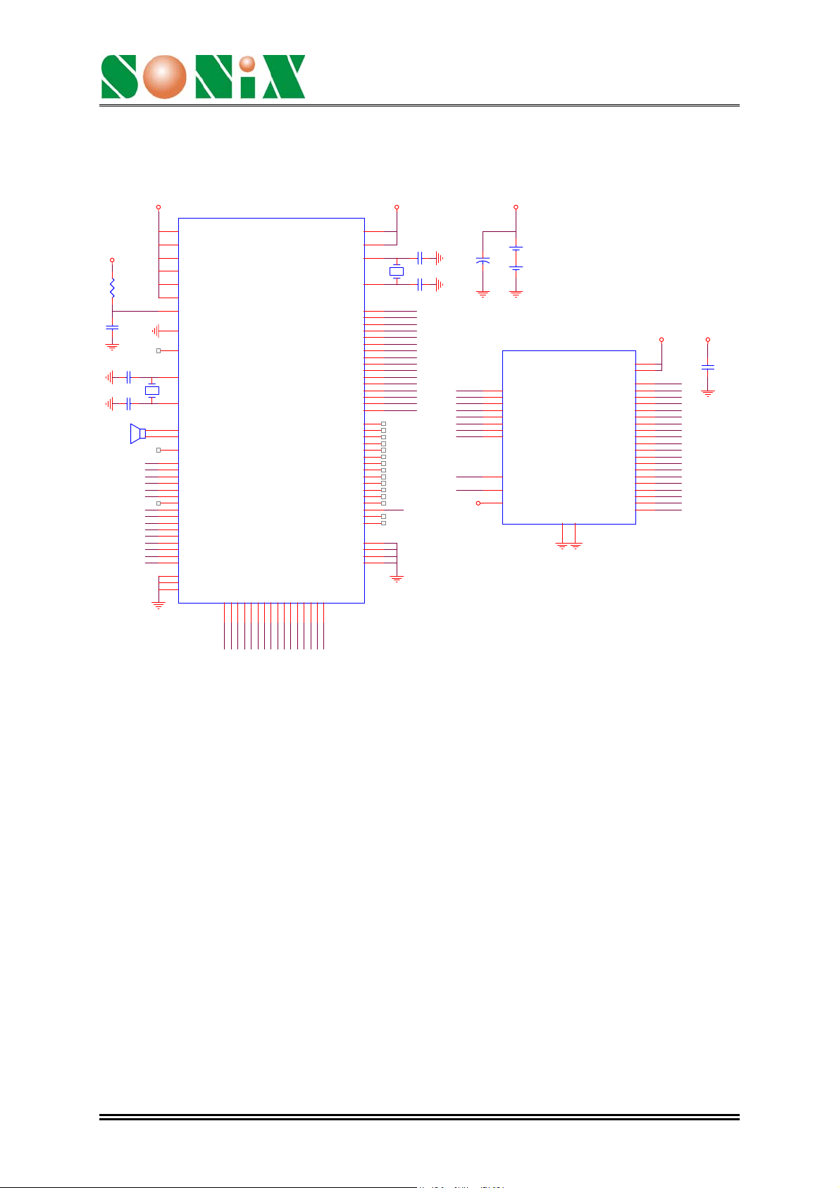
The SNR008 is a signal power, 8M-bit, read only memory. It is organized as 1M bytes,
operates for single 3V power supply, support static standby mode. The SNR008
embedded two different interfaces, one is a standard 8-bit interface bus which
compatible with SNL310, another one is a special 8-bit AD (address/data) bus which
compatible with SNC710.
SNR008 offers automatic power-down, with power-down controlled by the chip enable
“CE\”. When chip enable goes to high, SNR008 will entry power-down mode in order to
save the power consumption.
2. FEATURES
Power supply: 2.4V ~ 3.6V ♦
♦
Memory Size: 8M-bit
♦
Totally static operation
♦
Embedded a standard 8-bit bus interface compatible with SNL310 or a 8-bit AD
(address/data) bus interface compatible with SNC710
♦
Access time: 200ns @3V
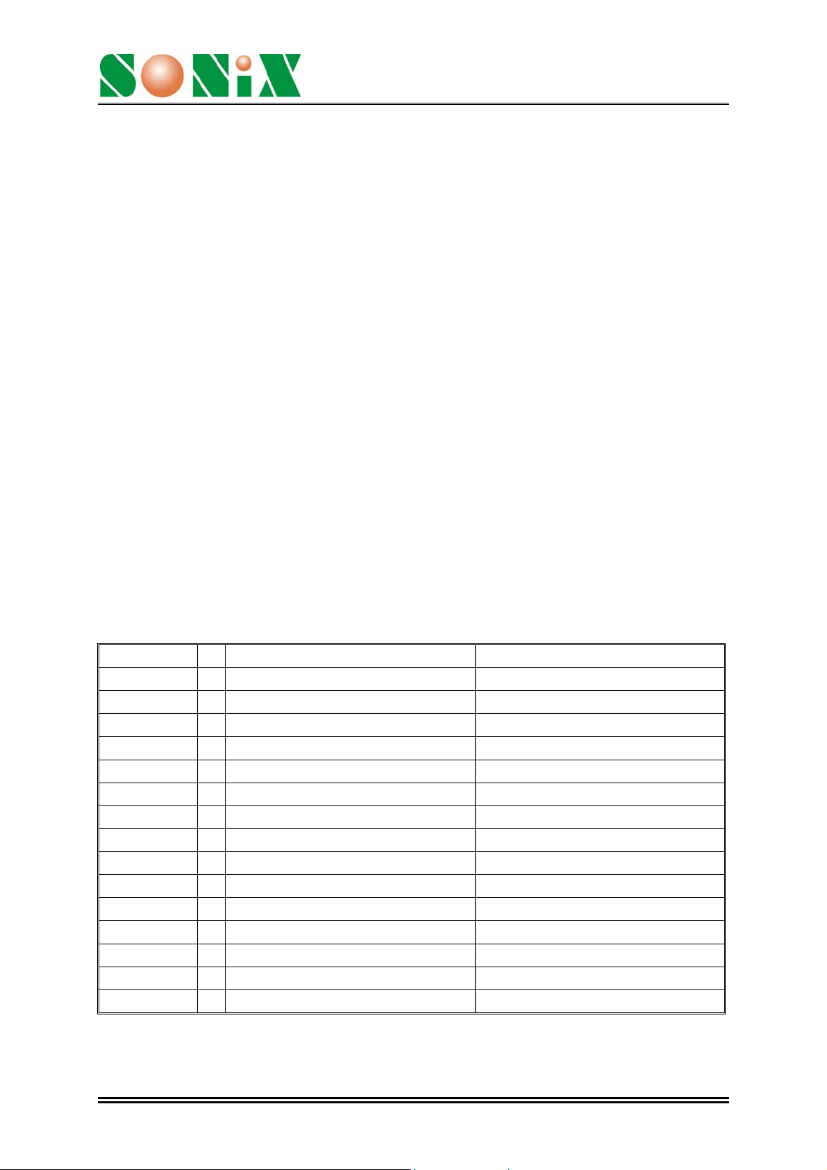
3. PIN ASSIGNMENTS
Symbol I/O Standard ROM interface AD Bus interface
TYPE I 1: Standard ROM type 0: AD Bus interface
A[8..19] I Standard ROM Address [8..19] NC
A[7] I Standard ROM Address A7 TESTM
A[6] I Standard ROM Address A6 Bank Select 4
A[5] I Standard ROM Address A5 Bank Select 3
A[4] I Standard ROM Address A4 Bank Select 2
A[3] I Standard ROM Address A3 Bank Select 1
A[2] I Standard ROM Address A2 Bank Select 0
A[1] I Standard ROM Address A1 ALECLK
A[0] I Standard ROM Address A0 READY
D[0..7] I/O Standard ROM Data [0..7] Address/Data bus [0..7]
CEB I Standard ROM Chip Enable Chip Enable
OEB I Standard ROM Output Enable NC
VDD P 3.3volt Positive Power supply 3.3volt Positive Power supply
GND P Ground Ground
Ver. 1.3
August 29, 2003
3
Page 4
SNR008
8M-bit Mask ROM
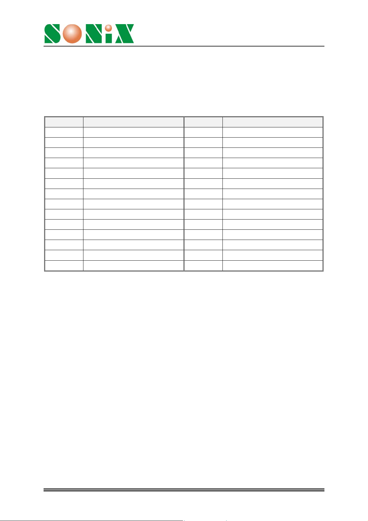
4. Memory mapping for AD Bus Interface
For 8-bit AD (address/data) bus interface, all the address and data communication
between SNC710 and SNR008 are through data bus D[0..7]. SNC710 allows user to
connect maximum 2 external mask ROM, and SNR008 has 5 bank select pins
(BS0~BS4) to specify the memory region of each mask ROM.
BS4~BS0 Address Region BS4~BS0 Address Region
00100 0x0200000 ~ 0x027FFFF 10010 0x0900000 ~ 0x097FFFF
00101 0x0280000 ~ 0x02FFFFF 10011 0x0980000 ~ 0x09FFFFF
00110 0x0300000 ~ 0x037FFFF 10100 0x0A00000 ~ 0x0A7FFFF
00111 0x0380000 ~ 0x03FFFFF 10101 0x0A80000 ~ 0x0AFFFFF
01000 0x0400000 ~ 0x047FFFF 10110 0x0B00000 ~ 0x0B7FFFF
01001 0x0480000 ~ 0x04FFFFF 10111 0x0B80000 ~ 0x0BFFFFF
01010 0x0500000 ~ 0x057FFFF 11000 0x0C00000 ~ 0x0C7FFFF
01011 0x0580000 ~ 0x05FFFFF 11001 0x0C80000 ~ 0x0CFFFFF
01100 0x0600000 ~ 0x067FFFF 11010 0x0D00000 ~ 0x0D7FFFF
01101 0x0680000 ~ 0x06FFFFF 11011 0x0D80000 ~ 0x0DFFFFF
01110 0x0700000 ~ 0x077FFFF 11100 0x0E00000 ~ 0x0E7FFFF
01111 0x0780000 ~ 0x07FFFFF 11101 0x0E80000 ~ 0x0EFFFFF
10000 0x0800000 ~ 0x087FFFF 11110 0x0F00000 ~ 0x0F7FFFF
10001 0x0880000 ~ 0x08FFFFF 11111 0x0F80000 ~ 0x0FFFFFF
Table-1
Note: For the address region 0x00000~0x01FFFFF are reserved, and the setting
of bank select pins BS4~BS0 CAN’T be the range 0000~0x0011.
Ver. 1.3
August 29, 2003
4
Page 5
SNR008
8M-bit Mask ROM
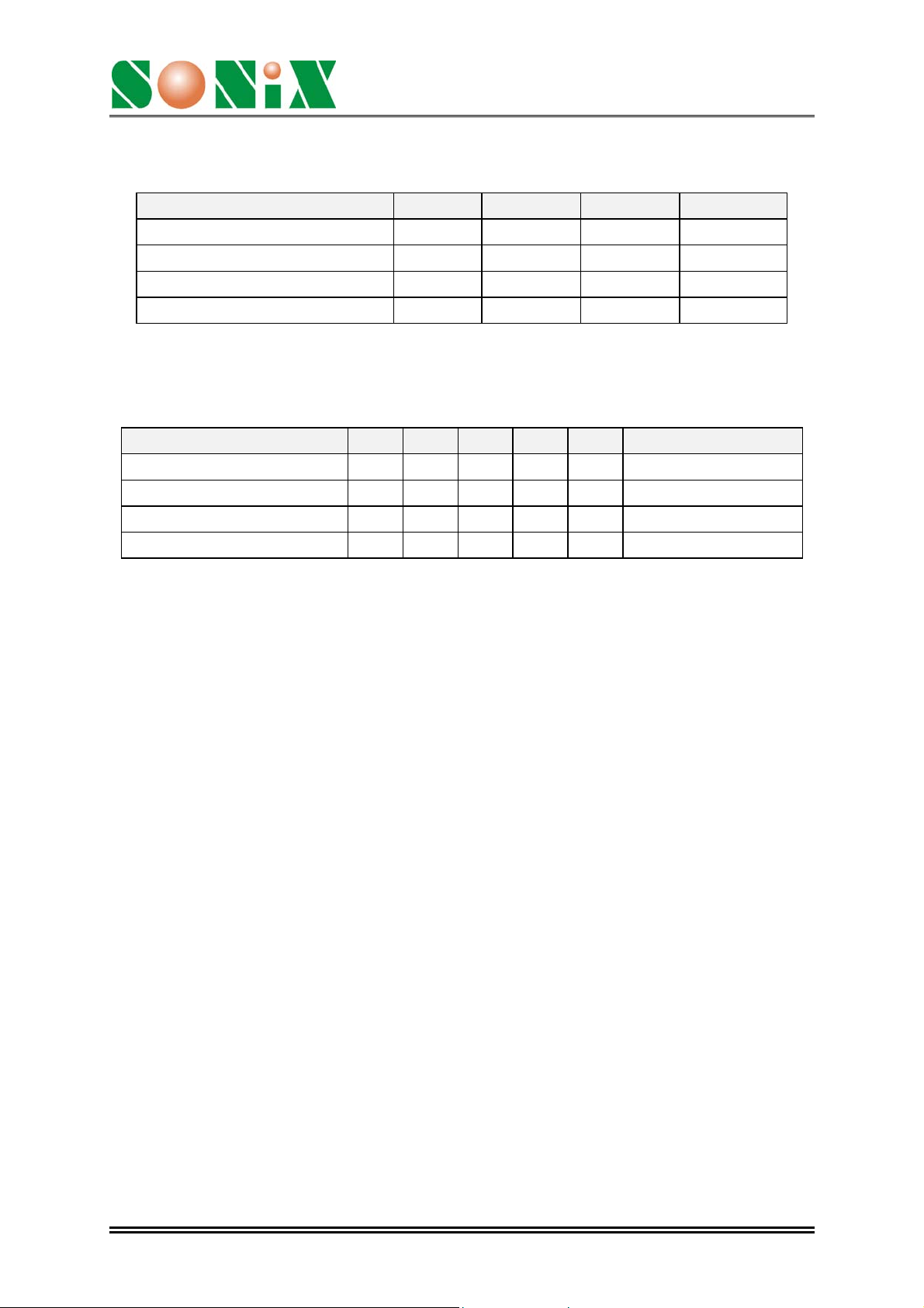
5. ABSOLUTE MAXIMUM RATINGS
Items Symbol Min Max Unit.
Supply Voltage VDD-V -0.3 6.0 V
Input Voltage VIN GND-0.3 VDD+0.3 V
Operating Temperature TOP 0 55 oC
Storage Temperature T
-55.0 125.0 oC
STG
6. ELECTRICAL CHARACTERISTICS
Item Sym. Min. Typ. Max. Unit Condition
Operating Voltage VDD 2.4 - 3.6 V
Standby current I
Operating Current I
Address access time tAA - - 200 ns Vdd=3V
- 1.5 2.0 uA VDD=3V, no load
SBY
- 4 - mA VDD=3V, no load
OPR
Ver. 1.3
August 29, 2003
5
Page 6
SNR008
8M-bit Mask ROM
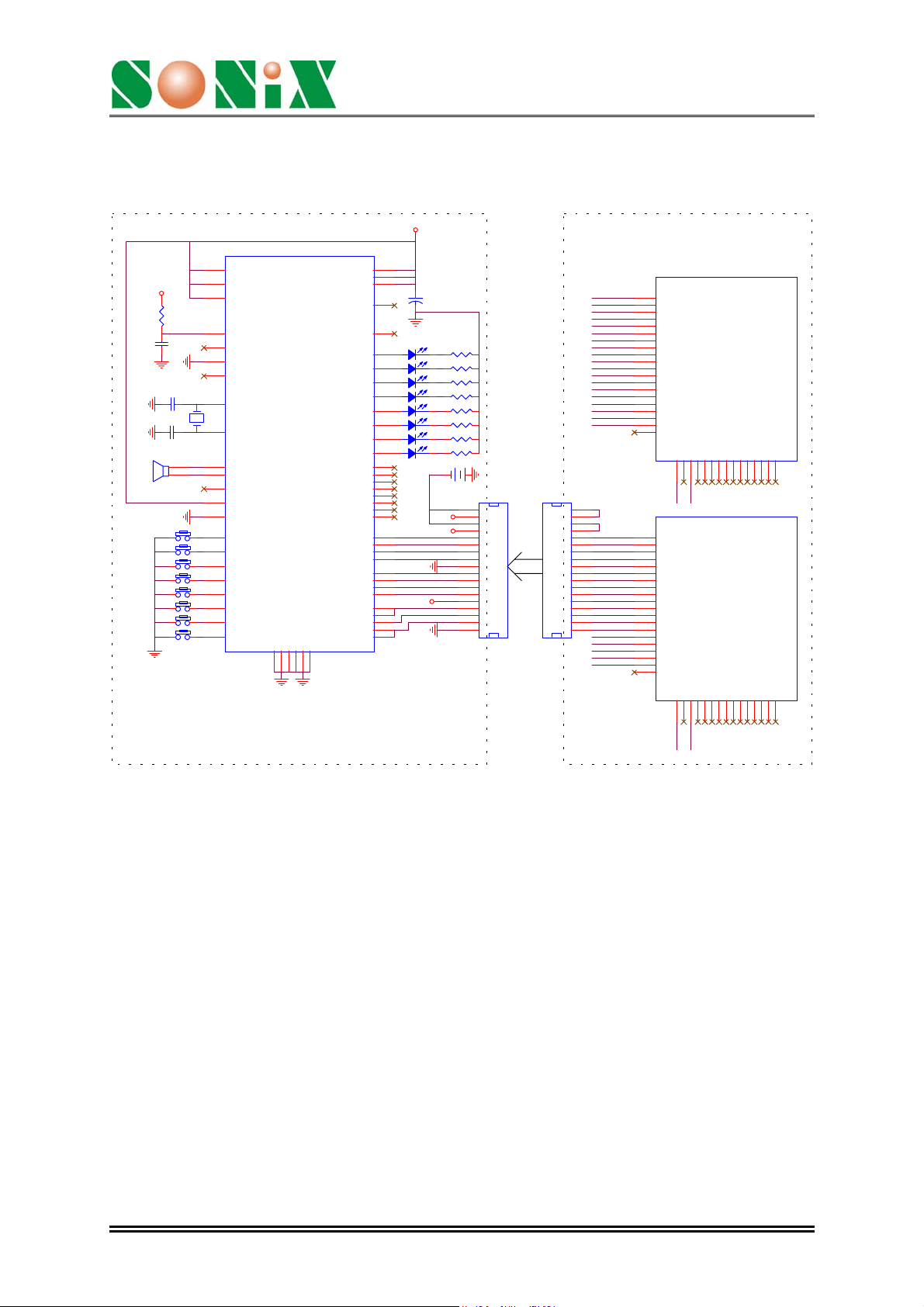
7. Application circuit
7.1 AD Bus Interface (with SNC710)
VDD3V
U1 SNC710
220K
0.1uF
SPEAKER
VDD3V
TR1
TR2
TR3
TR4
TR5
TR6
TR7
TR8
9
VDD
45
VDD
58
VDD
51
RST
49
TEST
48
CKSEL
20
15pF
15pF
EXTM
26
XIN
16MHZ
27
XOUT
44
BP0
46
BN0
24
VO
23
VDD
25
GND
10
P1.0
11
P1.1
14
P1.2
15
P1.3
16
P1.4
17
P1.5
18
P1.6
19
P1.7
GND13GND38GND43GND47GND52GND
59
CVDD
CVDD
CVDD
LXIN
LXOUT
P0.0
P0.1
P0.2
P0.3
P0.4
P0.5
P0.6
P0.7
P0.8
P0.9
P0.10
P0.11
P0.12
P0.13
P0.14
P0.15
CEB
CEIN
READY
ALECLK
CLKIN
12
33
53
22
47uF
21
50
54
55
56
57
60
61
62
1
2
3
4
5
6
7
8
42
AD0
41
AD1
40
AD2
39
AD3
37
AD4
36
AD5
35
AD6
34
AD7
32
31
30
29
28
VDD3V
330
330
330
330
330
330
330
330
VDD3V
VDD3V
3V
1
2
3
4
5
6
7
8
9
10
11
12
13
14
15
16
17
18
CONN 18
ROM Interface
CONN 18
AD0
AD1
AD2
AD3
GND
AD4
AD5
AD6
AD7
VDD3V
CE_
READY
ALECLK
GND
GND
GND
VDD3V
GND
GND
1
2
3
4
AD0
5
AD1
6
AD2
7
AD3
8
GND
9
AD4
10
AD5
11
AD6
12
AD7
13
VDD3V
14
CE_
15
READY
16
ALECLK
17
Extension ROM card
GND
18
VDD3V
GND
VDD3V
GND
GND
U1
ROM#1
1
AD0
2
0x200000-0x27FFFF
AD1
3
AD2
4
AD3
5
GND
6
AD4
7
AD5
8
AD6
9
AD7
10
VDD
11
CEB
12
READY
13
ALECLK
14
GND
15
BS0
16
BS1
17
BS2
18
BS3
19
BS4
20
TESTM
TYPE21NC22VDD23NC24NC25NC26NC27NC28NC29NC30NC31NC32NC33NC34NC
SNR008
VDD3V
VDD3V
U2
ROM#2
1
AD0
2
0x280000-0x2FFFFF
AD1
3
AD2
4
AD3
5
GND
6
AD4
7
AD5
8
AD6
9
AD7
10
VDD
11
CEB
12
READY
13
ALECLK
14
GND
15
BS0
16
BS1
17
BS2
18
BS3
19
BS4
20
TESTM
TYPE21NC22VDD23NC24NC25NC26NC27NC28NC29NC30NC31NC32NC33NC34NC
SNR008
35
35
VDD3V
VDD3V
Ver. 1.3
August 29, 2003
6
Page 7
SNR008
8M-bit Mask ROM
7.2 Standard ROM interface (with SNL310)
VDD
1.5V
C6
47uF
1.5V
VDD
VDD
BS1A3
A10
A11
A12
A13
A14
A15
A16
A17
A18
A19
A8
A9
SNR008
VDD
10
23
12
13
15
16
17
18
19
20
24
25
26
27
28
29
30
31
32
33
34
35
U2
1
AD0/D0
2
AD1/D1
3
AD2/D2
4
AD3/D3
6
AD4/D4
7
AD5/D5
8
AD6/D6
9
AD7/D7
11
CEB
22
OEB
21
TYPE
READYB/A0
ALECLK/A1
BS0/A2
BS2/A4
BS3/A5
BS4/A6
TESTM/A7
GND
GND
5
14
VDD
C7
A0
A1
A2
A3
A4
A5
A6
A7
A8
A9
A10
A11
A12
A13
A14
A15
A16
A17
A18
A19
0.1uF
VDD
R1
220K
RST
C1
0.1uF
15pF
15pF
SPEAKER
VDD
U1
SNL310
3
VDD
19
VDD
37
VDD
48
VDD
60
VDD
79
VDD
83
RST
52
CKSEL
53
A16
A17
A18
A19
A20
A21
RDB
D0
D1
D2
D3
D4
D5
D6
D7
TESTM
6
XIN
Y1
7
XOUT
47
BP0
49
BN0
4
VO
25
P5.0
24
P5.1
23
P5.2
22
P5.3
21
P5.4
20
P5.5
18
P5.6
16
P5.7
15
P5.8
14
P5.9
13
P5.10
12
P5.11
11
P5.12
10
P5.13
9
P5.14
8
P5.15
5
GND
17
GND
28
GND
P4.1527P4.1429P4.1330P4.1231P4.1132P4.1033P4.934P4.8
35
36
C2
16MHZ
C3
CVDD
CVDD
LXIN
LXOUT
P2.0
P2.1
P2.2
P2.3
P2.4
P2.5
P2.6
P2.7
P2.8
P2.9
P2.10
P2.11
P2.12
P2.13
P2.14
P2.15
P3.0
P3.1
P3.2
P3.3
P3.4
P3.5
P3.6
P3.7
P3.8
P3.9
P3.10
P3.11
P3.12
P3.13
P3.14
P3.15
GND
GND
GND
GND
P4.045P4.144P4.243P4.342P4.440P4.539P4.638P4.7
VDD
26
85
2
1
90
89
88
87
86
82
81
80
78
77
76
75
74
73
72
71
70
69
68
67
66
65
64
63
61
59
58
57
56
55
54
51
41
46
84
50
Y2
P2_0
P2_1
P2_2
P2_3
P2_4
P2_5
P2_6
P2_7
P2_8
P2_9
P2_10
P2_11
P2_12
P2_13
P2_14
P2_15
CEB
C4
32768HZ
C5
15pF
15pF
D0
D1
D2
D3
D4
D5
D6
D7
CEB
RDB
VDD
A0A2A1A6A4
A3
A5
A7A8A9
A10
A11
A12
A13
A14
A15
Ver. 1.3
August 29, 2003
7
Page 8
SNR008
8M-bit Mask ROM
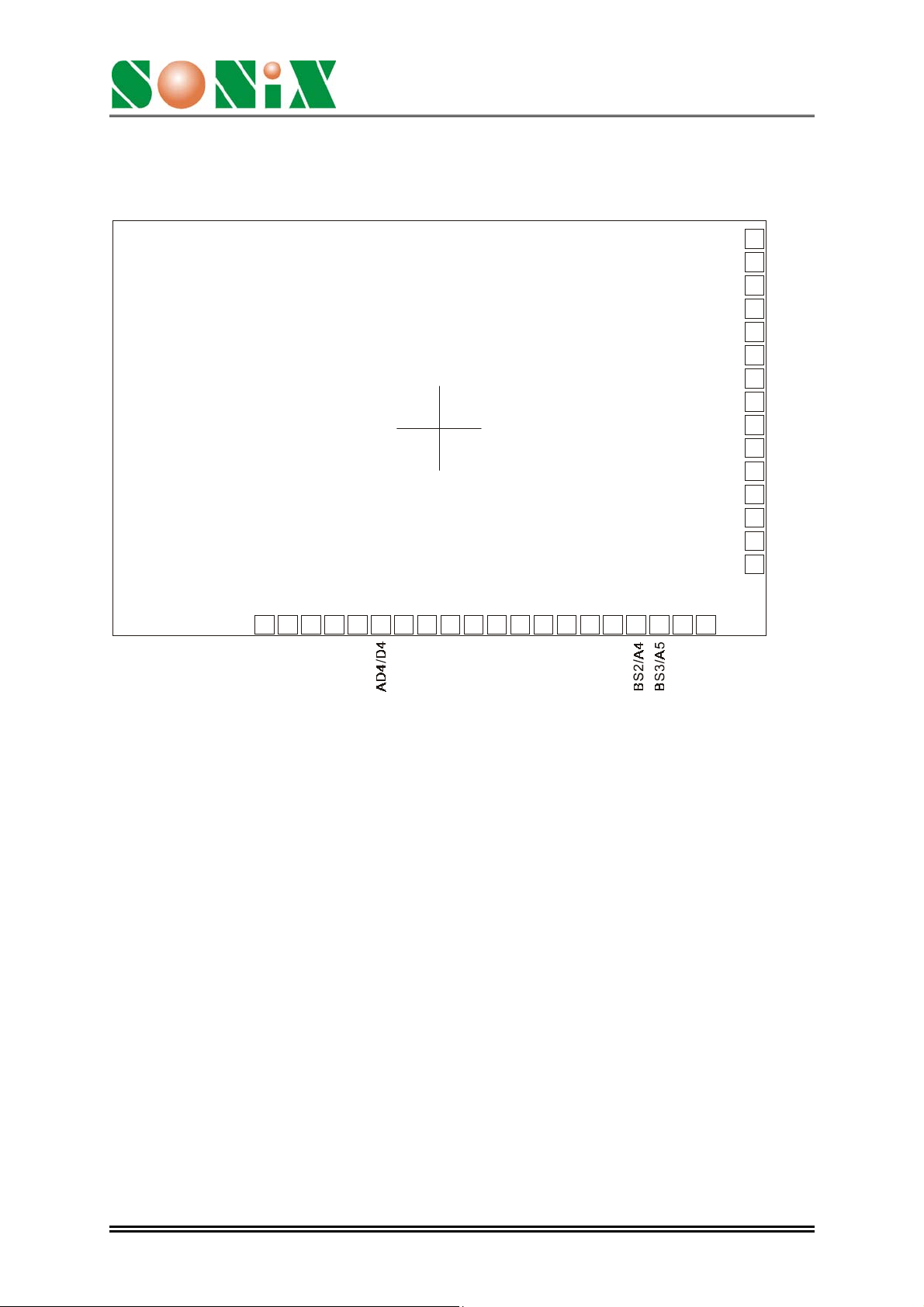
8. BONDING PAD
35
A19
34
A18
33
A17
A16
32
31
A15
30
A14
A13
29
A12
28
(0.00,0.00)
27
26
25
24
23
22
21
A11
A10
A9
A8
VDD
OEB
TYPE
123456 7 8910111213141516171819
CEB
AD0/D0
GND
AD1/D1
AD2/D2
AD3/D3
AD6/D6
AD5/D5
VDD
AD7/D7
READY/A0
GND
BS0/A2
BS1/A3
ALECLK/A1
Note: The substrate MUST be connected to Vss in PCB layout.
20
BS4/A6
TESTM/A7
Ver. 1.3
August 29, 2003
8
Page 9

SNR008
8M-bit Mask ROM
DISCLAIMER
The information appearing in SONiX web pages (“this publication”) is believed to be
accurate.
However, this publication could contain technical inaccuracies or typographical errors.
The reader should not assume that this publication is error-free or that it will be
suitable for any particular purpose. SONiX makes no warranty, express, statutory
implied or by description in this publication or other documents which are referenced
by or linked to this publication. In no event shall SONiX be liable for any special,
incidental, indirect or consequential damages of any kind, or any damages whatsoever,
including, without limitation, those resulting from loss of use, data or profits, whether or
not advised of the possibility of damage, and on any theory of liability, arising out of or
in connection with the use or performance of this publication or other documents which
are referenced by or linked to this publication.
This publication was developed for products offered in Taiwan. SONiX may not offer
the products discussed in this document in other countries. Information is subject to
change without notice. Please contact SONiX or its local representative for
information on offerings available. Integrated circuits sold by SONiX are covered by
the warranty and patent indemnification provisions stipulated in the terms of sale only.
The application circuits illustrated in this document are for reference purposes only.
SONIX DISCLAIMS ALL WARRANTIES, INCLUDING THE WARRANTY OF
MERCHANTABILITY OR FITNESS FOR ANY PURPOSE. SONIX reserves the right
to halt production or alter the specifications and prices, and discontinue marketing the
Products listed at any time without notice. Accordingly, the reader is cautioned to
verify that the data sheets and other information in this publication are current before
placing orders.
Products described herein are intended for use in normal commercial applications.
Applications involving unusual environmental or reliability requirements, e.g. military
equipment or medical life support equipment, are specifically not recommended
without additional processing by SONIX for such application.
Ver. 1.3
August 29, 2003
9
 Loading...