

Page 1
SN6B000
Hi-Density LCD Driver with 8-bit Controller
GENERAL DESCRIPTIONS
SN6B000 is a 8-bit micro controller series with hi-density LCD driver. Combined
with one or more SN6BS00 (64-segment drivers), SN6B000 can form one 1024/
2048/ 4096/ 6144/ 8192 dots LCD system. A dual-tone melody and a voice
synthesizer are included in SN6B000. Also, a 7-bit current-type DAC and the
PWM circuit are built in SN6B000, so that makes users easily choose a speaker
(DA), or a buzzer (PWM) for their applications. SN6B000 only contains 32 COM
signals of LCD. All segment signals are provided by SN6BS00. Several
different types of LCD applications can be implemented by suitably combining
SN6B000 and SN6BS00. SN6B000 not only contains internal mask ROM itself
(128K words, MC mode), but also possesses the interface to access external
ROM (maximum 512K words, MP mode). A memory chip, SN6B400 consists of
256K-word mask ROM and is available to work with SN6B000 to accomplish the
whole micro-processor system.
Dots Configuration COM SEG
1024
2048
4096
6144
8192
1 SN6B000 + l SN6BS00
1 SN6B000 + l SN6BS00
1 SN6B000 + 2 SN6BS00
1 SN6B000 + 3 SN6BS00
1 SN6B000 + 4 SN6BS00
16 64
32 64
32 128
32 192
32 256
1
December 20, 2000
Page 2
Hi-Density LCD Driver with 8-bit Controller
FEATURES
ROM space: 512K words (=219*16=220*8); Program Space: 256K*16
MC mode:128K words in SN6B000
−
MP mode: along with SN6B400 to 256K words
−
RAM Size:
256 bytes in SN6B000
−
4*256 bytes in SN6BS00 (2*256 bytes LCD RAM, 2*256 bytes normal
−
RAM)
I/O Port : There are Port0 and Port1 (total 16 pins I/O)
All ports are I/O-type and P0.7 can be modulated with a carry signal
−
Each port can be set as “H”, ”L”,
−
(150K@5V
Every port can wake up chip when chip is in power-down mode
−
60 instructions
8 levels stack buffer supports interrupt and call subroutine
System Clock:
2MHz RC oscillator
−
2M/ 4M(3.58M) crystal
−
Low speed clock: Register option, 32768 crystal or RC
Three different operation modes can be selected:
Normal mode (both High/Low osc. On).
−
Slow mode (High osc. Off, Low osc. On).
−
Stop mode (both High and Low osc. Off).
−
LCD: 1/16 duty (for 1024) or 1/32 duty, frame rate=64 or 128 Hz.
A voltage regulator and double voltage circuit is included in SN6BS000
8 interrupt sources :
5 internal interrupts: T0, TC0, TC1, TW, SPEECH (non-maskable).
−
3 external interrupts: INTP0.0 ~ INTP0.2
−
ISR entry location: Reset: 0000, SPEECH: 0018h, and the others: 0008h
−
Voice:
Built-in voice synthesizer
−
Sampling rate from 4K to 40Khz
−
Dual tone melody with 4 octaves
−
7-bit DA converter (maximum 3mA)
−
PWM output for Buzzer
−
)
floating
, and
high-resistance “H”
SN6B000
2
December 20, 2000
Page 3
Hi-Density LCD Driver with 8-bit Controller
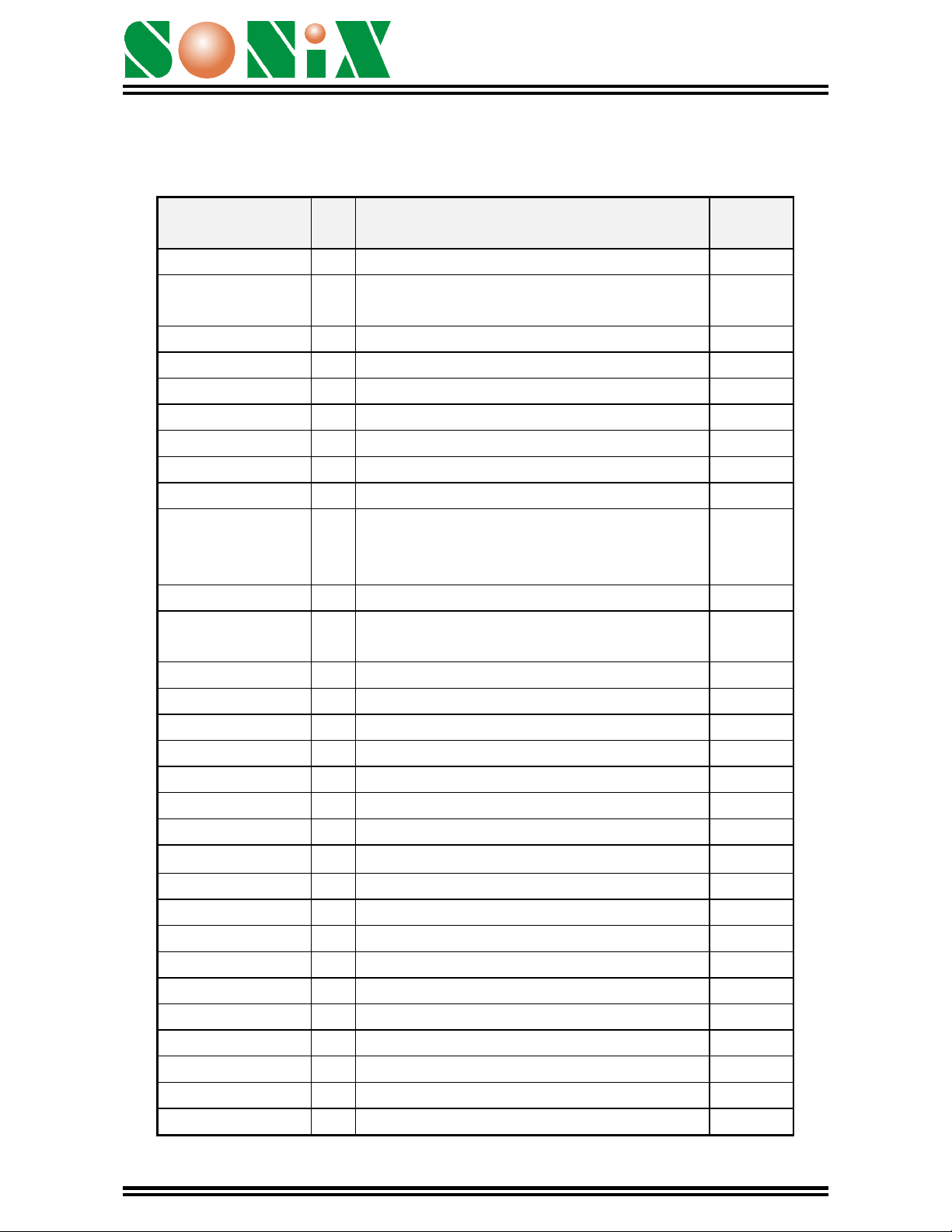
PIN ASSIGNMENT
SN6B000
Pin Name I/O Descriptions Internal
C0~C31 O Common 0 ~ 31
VLC1, VLC4,
VLC5
VLCDR I LCD Bias
P/C I Micro-processor/Micro-controller
A0~A19 O Address Bus for ROM
D0~D7 I/O Data Bus for ROM
CE1B O Chip Enable of External ROM.
VO/ BUZ1 O Voice out, 7-bit DA / PWM output
BUZ2 O PWM output
OSC/XIN High speed Clock input:
XOUT O High Speed clock output
CKSEL I High speed clock selection
LXIN I Low speed clock input
LXOUT O Low speed clock output
P0, P1 I/O I/O Ports
XCE_0 O Chip Enable of SN6BS00 0
XCE_1 O Chip Enable of SN6BS00 1
XCE_2 O Chip Enable of SN6BS00 2
XCE_3 O Chip Enable of SN6BS00 3
XD7~XD0 I/O Data Bus to Slave Driver
I LCD Bias
CKSEL=L, RC oscillator
CKSEL=H, Crystal
( 0:2M RC oscillator, 1: Crystal)
SN6B000
Pull-low
√
√
XA9~XA0 O Address Bus to Slave Driver
WR O Read Write signal
FRAME O Frame Synchronous Signal
CL O Display Synchronous Signal
M O Alternating signal for LCD
SYNC O Phase 1 synchronous pin.
TEST I Test Pin
RESETB I Reset Pin
VDD I Positive power supply
GND I Negative power supply
3
√
December 20, 2000
Page 4
Hi-Density LCD Driver with 8-bit Controller
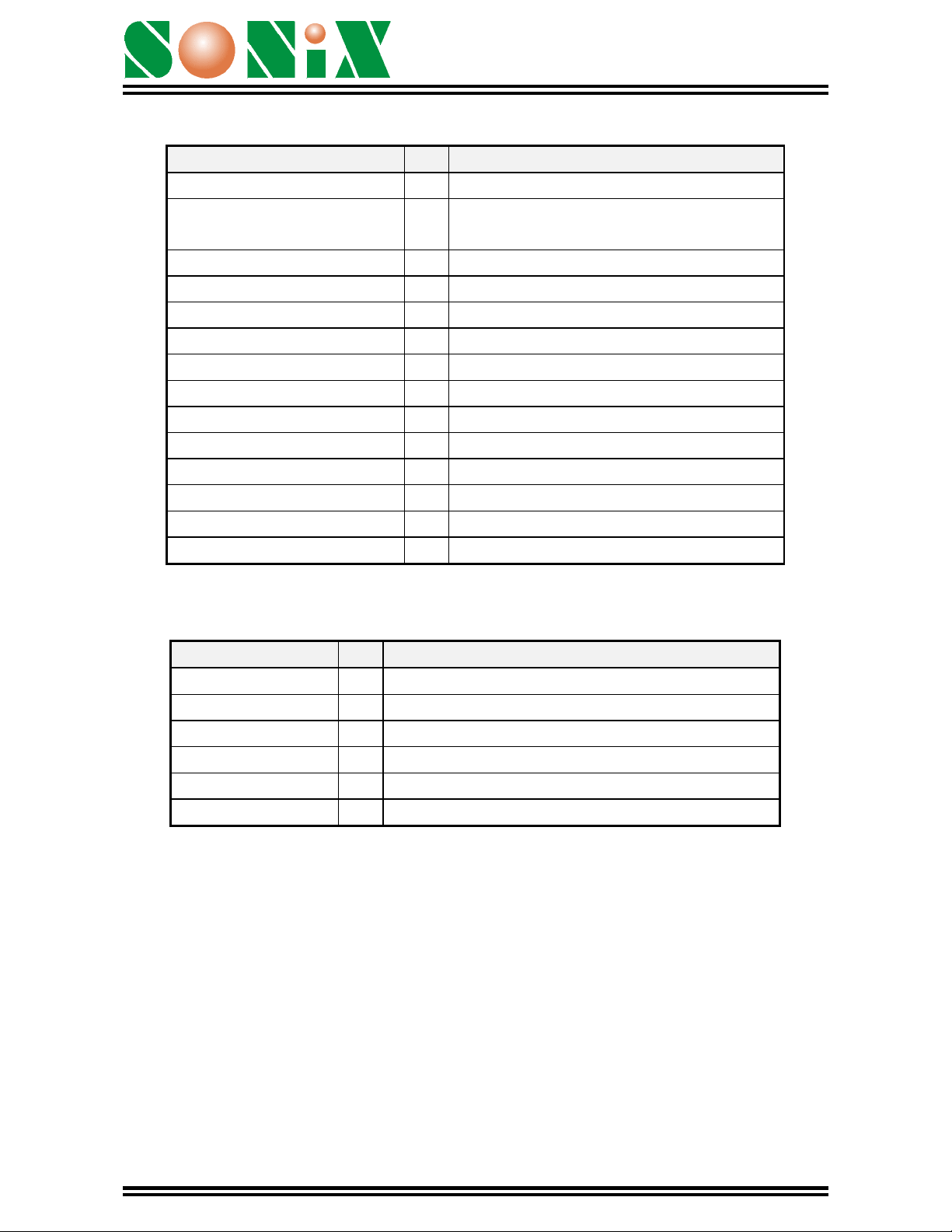
SN6BS00:
Pin Name I/O Descriptions
S0~S63 O Segment 0 ~ 63
VLCDR, VLC2, VLC3,
I LCD Bias
VLC5
VREG O Voltage Pumper
VPS I Voltage Pumper
VO1, VO2 I Voltage Pumper
XA0~XA9 I Address Bus
XD0~XD7 I/O Data Bus
XCE I Chip Enable
WR I Read Write signal
FRAME I Frame Synchronous Signal
CL I Display Synchronous Signal
M I Alternating signal for LCD
VDD I Positive power supply
GND I Negative power supply
SN6B000
SN6B400:
Pin Name I/O Function Description
V
DD
I Positive power supply
CEB I Chip Enable. (Active Low)
SYNC I Clock Pin
D7~D0 O Data Output
A18~A0 I Address Input
VSS I Negative power supply.
4
December 20, 2000
Page 5

SN6B000
Hi-Density LCD Driver with 8-bit Controller
ABSOLUTE MAXIMUM RATINGS
(All of the voltages referenced to Vss)
Supply voltage (Vdd) - 0.3V ~ 6.0V
Input in voltage (Vin) Vss - 0.2V ~ Vdd + 0.2V
Operating ambient temperature (Topr) 0°C ~ + 70°C
Storage ambient temperature (Tstor) -30°C ~ + 125°C
Power consumption (Pc) 500 mW
ELECTRICAL CHARACTERISTICS
SN6B000
PARAMETER SYM. DESCRIPTION MIN. TYP. MAX. UNIT
Operating v oltage Vdd 3.9 - 5.1 V
Operating current IddH Vdd = 5.0V, I/O pin unload, normal
mode
Idds Vdd = 5.0V,I/O pin unload, slow
mode
Istby Vdd = 5.0V,I/O pin unload, stop
mode
Reset, TEST pin ViH 0.7Vdd - - V
input voltage ViL - - 0.3Vss
Reset, TEST leakage
current
I/P port input voltage ViH 0.8Vdd - - V
I/P port pull-up resistor Rup Vin = Vss - 150 - K
I/P port input leakage
current
Port0,1 output source
Current
Port0,1 output sink
Current
LCD supply voltage Vlcd - - 6.5 V
LCD frame frequency Flcd - 64/128 - Hz
Vo output Current Ivo DA output current - 3 4 mA
BU1,BU2 Driving
Current
BU1,BU2 Sinking
Current
INTP0 trigger pulse
width
Oscillator frequency fHxosc Rosc=300K
ILekg Vin = Vdd - - 1 uA
ViL - - 0.2Vss
Ilekg Pull-up resistor disable, Vin = Vdd - - 1 uA
IoH Vop = Vdd - 0.5V 1 2 - mA
IoL Vop = Vss + 0.5V 2 4 - mA
IdBU PWM driving current ability.
V
IsBU PWM sinking current ability.
V
Tint01 P0.0 ~ P0.2 Interrupt request pulse
width
BU1/BU2
BU1/BU2
=2.5V
=2.5V
Ω
-1-mA
-15-uA
--1uA
-60-mA
-60-mA
1/fcpu - - S
-2-MHz
Ω
5
December 20, 2000
Page 6

SN6B000
Hi-Density LCD Driver with 8-bit Controller
SN6BS00
(All of voltages referenced to Vss, Vdd = 5.0V, SN6B000@3.58MHz, ambient temperature is 25°C unless
otherwise note.)
PARAMETER SYM. DESCRIPTION MIN. TYP. MAX. UNIT
Operating v oltage Vdd 3.9 - 5.1 V
Operating current IddH LCD pin unload, Voltage-doubler ON - 3 - mA
Standby Current Istby LCD pin unload, Voltage-doubler
OFF,
No Data Access from SN6B000.
Output Voltage of VREG V
VDD=3.9V - 5.4 - V
OREG
VDD=4.5V - 5.9 - V
VDD=5.1V - 6.2 - V
SN6B400
--1uA
(All of voltages referenced to Vss, Vdd = 5.0V, SN6B000@3.58MHz, ambient temperature is 25°C unless
otherwise note.)
PARAMETER SYM. DESCRIPTION MIN. TYP. MAX. UNIT
Operating v oltage Vdd 3.6 - 5.1 V
Operating current IddH - 400 - uA
Standby Current Istby CEB=5V - - 1 uA
Access time Tac Loading=10pf, VDD = 3.6V~5V - - 300 nS
6
December 20, 2000
Page 7

APPLICATION CIRCUIT
MC mode with 2048-dot (64 seg X 32 com, 1/7 bias) LCD
Clock: RC type (CPU frequency: 2MHZ)
−
No low speed clock
−
Speaker voice output
−
SN6B000
Hi-Density LCD Driver with 8-bit Controller
7
December 20, 2000
Page 8

Hi-Density LCD Driver with 8-bit Controller
MP mode with SN6B400 and 2048-dot (64seg X 32com, 1/7 bias)
LCD
Clock: 3.58MHZ crystal (CPU frequency: 3.58MHZ)
−
32768 low speed clock
−
Buzzer voice output
−
SN6B000
8
December 20, 2000
Page 9

SN6B000
Hi-Density LCD Driver with 8-bit Controller
MP mode with SN6B400 and 4096-dot (128seg X 32com, 1/7 bias)
LCD
−
Clock: 3.58MHZ (CPU frequency: 3.58MHZ)
−
32768 low speed clock
−
Speaker voice output
9
December 20, 2000
Page 10

BONDING PAD
Note : The substrate MUST be connected to Vss in PCB layout.
SN6B000
Hi-Density LCD Driver with 8-bit Controller
SN6B000
10
December 20, 2000
Page 11

Note : The substrate MUST be connected to Vss in PCB layout.
SN6B000
Hi-Density LCD Driver with 8-bit Controller
SN6BS00
11
December 20, 2000
Page 12

SN6B000
Hi-Density LCD Driver with 8-bit Controller
SN6B400
Note : The substrate MUST be connected to Vss in PCB layout.
12
December 20, 2000
Page 13

SN6B000
Hi-Density LCD Driver with 8-bit Controller
DISCLAIMER
The information appearing in SONiX web pages (“this publication”) is believed to be
accurate.
However, this publication could contain technical inaccuracies or typographical
errors.
The reader should not assume that this publication is error-free or that it will be
suitable for any particular purpose. SONiX makes no warranty, express, statutory
implied or by description in this publication or other documents which are referenced
by or linked to this publication. In no event shall SONiX be liable for any special,
incidental, indirect or consequential damages of any kind, or any damages
whatsoever, including, without limitation, those resulting from loss of use, data or
profits, whether or not advised of the possibility of damage, and on any theory of
liability, arising out of or in connection with the use or performance of this
publication or other documents which are referenced by or linked to this publication.
This publication was developed for products offered in Taiwan. SONiX may not
offer the products discussed in this document in other countries. Information is
subject to change without notice. Please contact SONiX or its local representative
for information on offerings available. Integrated circuits sold by SONiX are covered
by the warranty and patent indemnification provisions stipulated in the terms of sale
only.
The application circuits illustrated in this document are for reference purposes only.
SONIX DISCLAIMS ALL WARRANTIES, INCLUDING THE WARRANTY OF
MERCHANTABILITY OR FITNESS FOR ANY PURPOSE. SONIX reserves the right
to halt production or alter the specifications and prices, and discontinue marketing
the Products listed at any time without notice. Accordingly, the reader is cautioned
to verify that the data sheets and other information in this publication are current
before placing orders.
Products described herein are intended for use in normal commercial applications.
Applications involving unusual environmental or reliability requirements, e.g. military
equipment or medical life support equipment, are specifically not recommended
without additional processing by SONIX for such application.
13
December 20, 2000
 Loading...