

Page 1

SN6A296
LCD Controller with Voice/Dual Tone Melody
INTRODUCTION
SN6A296 is a series of single chip voice/dual tone melody synthesizer IC with
16*33/8*40/4*40 direct drive capability which contains two 4-bit I/O ports and a tiny
controller. By programming through the tiny controller, user’s application including
LCD display, section combination, trigger modes, output status, voice/melody
playing and other logic functions and then be easily implemented.
FEATURES
Single power supply 2.4V – 5.1V
Built in a tiny controller
Two 4-bit I/O ports are provided, two optional 4-bit output ports are provided
256*4 bits RAM for programming usage are provided
160*4 bits RAM for LCD display usage are provided
Maximum 108k*10 program ROM is provided
Readable ROM code data
Built in direct 16*33/8*40/4*40 LCD driver
LCD 1/4 bias, 1/5 bias; 1/8 duty, 1/16 duty
Built in a high quality speech synthesizer
Adaptive playing speed from 2.5k-40kHz is provided
Built in a dual tone melody generator
Speech/Dual tone melody mixer is provided which SN6A296 can play speech
and dual tone melody simultaneously
Fixed current D/A output is provided to drive external connected transistor for
sound output
PWM output is provided to drive external connected piezo buzzer
Version: 1.01 September 26, 2002
1
Page 2
LCD Controller with Voice/Dual Tone Melody
PIN ASSIGNMENT
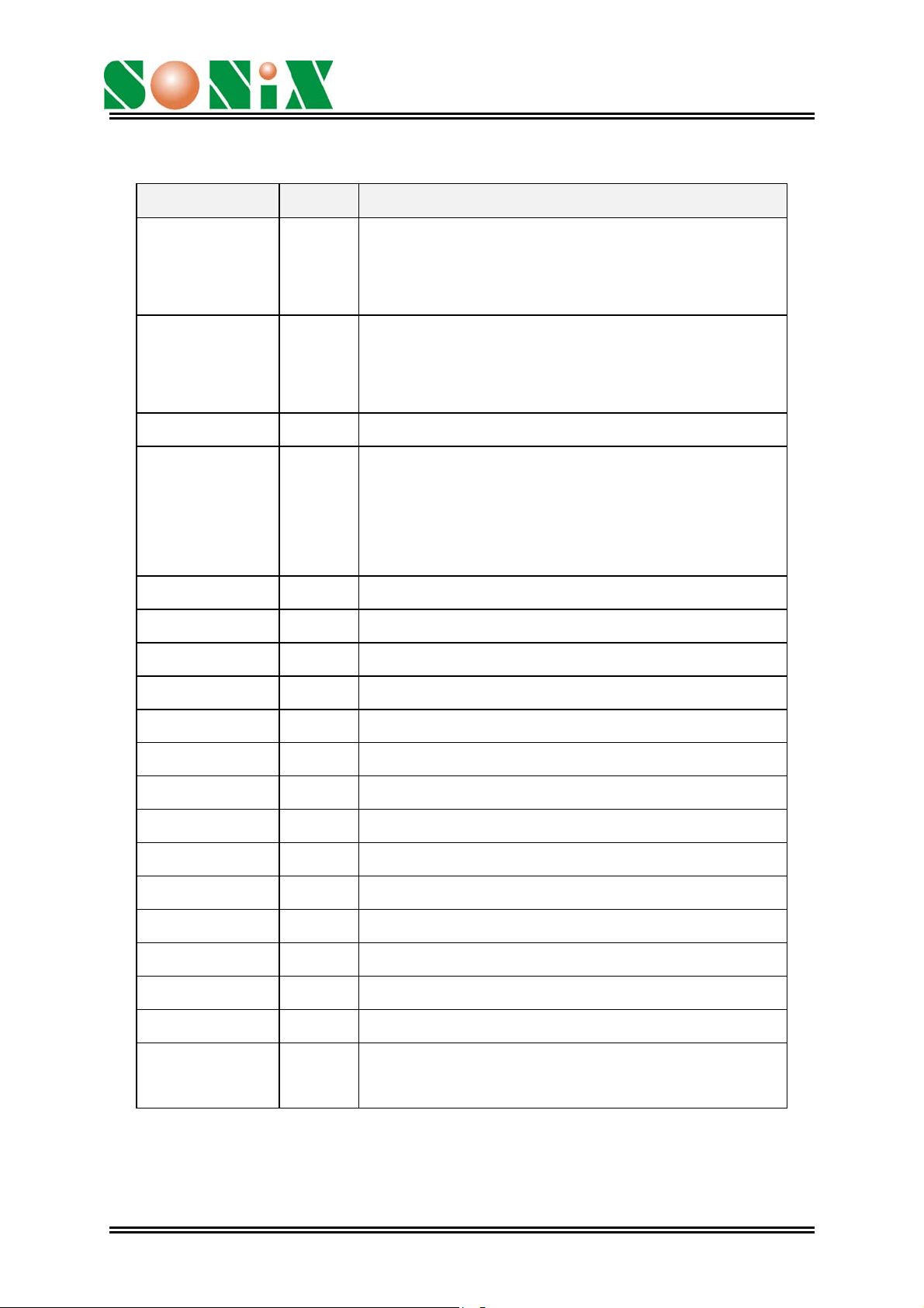
Symbol I/O Function Description
SEG1-SEG4 O Optional to be segment1~4 or P40~P43
SEG1~4: segment1~4 for LCD driver.
P40~P43: bit0-bit3 for output port 4.
SEG5-SEG8 O Optional to be segment5~8 or P50~P53
SEG5~8: segment5~8 for LCD driver.
P50~P53: bit0-bit3 for output port 5.
SEG9-SEG33 O Segment 9 ~ segment 33 for LCD driver
SN6A296
SEG34/COM16-
SEG40/COM10
COM9 O Com9 for 16*33 LCD driver.
COM8-COM1 O Com8-Com1 for 16*33/8*40/4*40 LCD driver.
GND I Negative power supply.
P33-P30 I/O Bit 3 to bit 0 of IO port 3.
P23-P20 I/O Bit 3 to bit 0 of IO port 2.
BU1,BU2 O Buzzer driver outputs.
VO O D/A current output.
RESET I Reset pin with internal pull low.
OSC I Oscillation component connection pin.
TEST I For testing only.
O Optional to be SEG34~40 or COM16~10
SEG34~40: segment34~40 for 8*40/4*40 LCD
driver.
COM16-10: com16~com10 for 16*33 LCD driver.
XIN,XOUT 32768 Hz Crystal connection pins.
VDD I Positive power supply.
VLCDR LCD voltage adjusting pin.
VLC1-VLC5 LCD voltage bias connection pins.
WSUB I Well substrate of chip. Connected to the highest
voltage of chip (VDD or VLCDR).
Version: 1.01 September 26, 2002
2
Page 3
LCD Controller with Voice/Dual Tone Melody
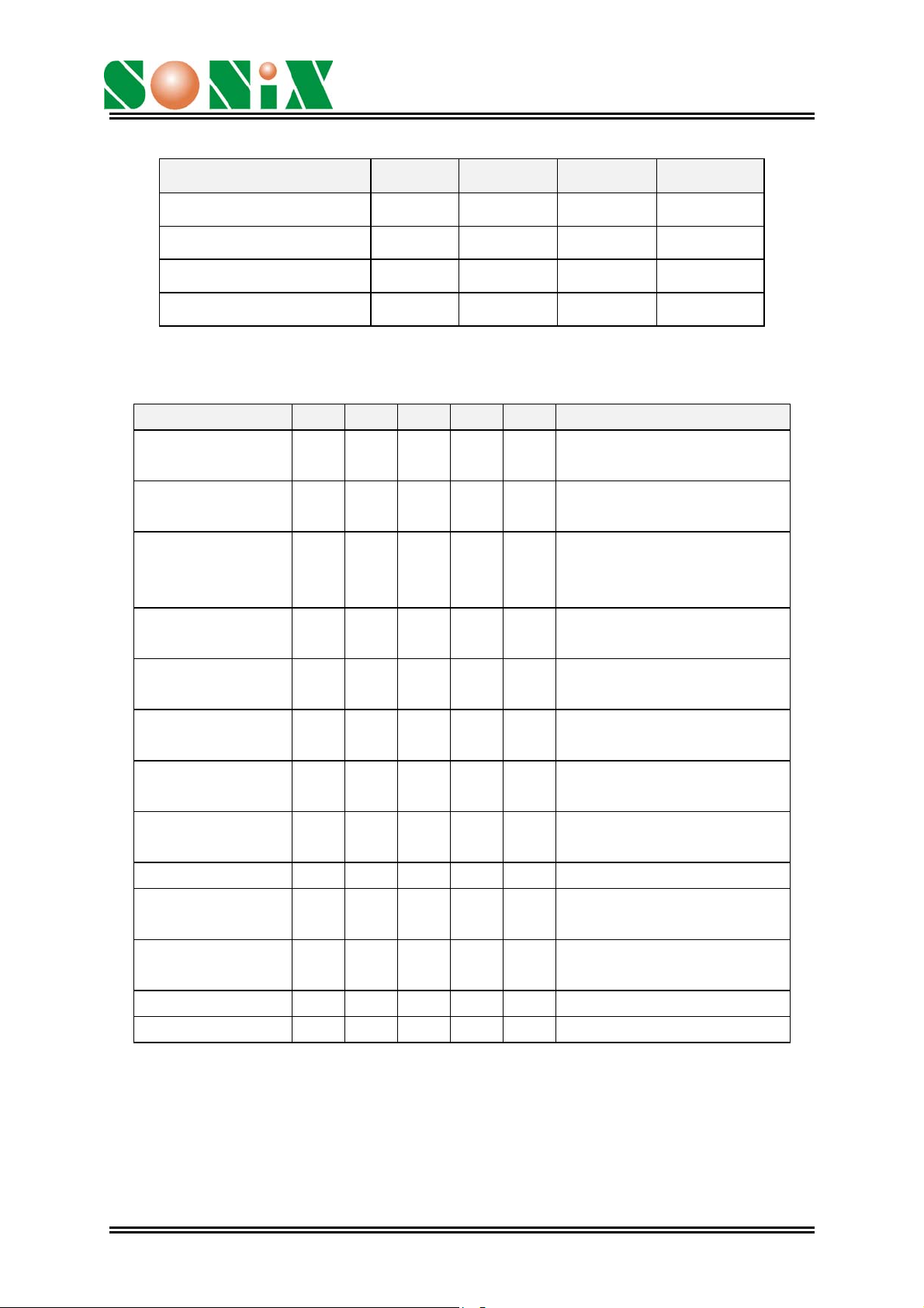
ABSOLUTELY MAXIMUM RATING
Items Symbol Min Max Unit.
Supply Voltage VDD-V -0.3 6.0 V
Input Voltage VIN VSS-0.3 VDD+0.3 V
Operating Temperature TOP -20.0 70.0 oC
SN6A296
Storage Temperature T
STG
ELECTRICAL CHARACTERISTIC
Item Sym. Min. Typ. Max. Unit Condition
Operating
Voltage
Standby current 1 I
Standby current 2 I
Operating
current
Input current
of ,P2,P3
Drive current
of P2,P3,P4,P5
large Sink current
of P2,P3,P4,P5
Small Sink current
of P2,P3,P4,P5
D/A output current IVO 2.0 3.0 4.0 mA VDD=3V,VO=0.7V
Buzzer drive
current
Buzzer sink
current
Oscillation resistor R - 1.0 - MHZ VDD=3V
Oscillation Freq. F
VDD 2.4 3.0 5.1 V
- - 1.0 uA VDD=3V,both system clk
SBY1
- 20 50 uA VDD=3V, system clk is off,
SBY2
I
- 350 500 uA VDD=3V, no load
OPR
IIH - 3.0 10.0 uA VDD=3V,VIN=3V
IOD -1.5 -2 - mA VDD=3V,VO=2.6V
I
2.0 3 - mA VDD=3V,VO=0.4V
OS1
I
- 0.4 - uA VDD=3V,VO=0.4V
OS2
I
-15 mA VDD=3V,VO=1.5V
BZD
I
15 mA VDD=3V,VO=1.5V
BZS
- 1.0 - MHZ VDD=3V
OSC
-55.0 125.0 oC
and 32768 Hz clk are off
32768 Hz clk is on for LCD
display and timer.
Version: 1.01 September 26, 2002
3
Page 4
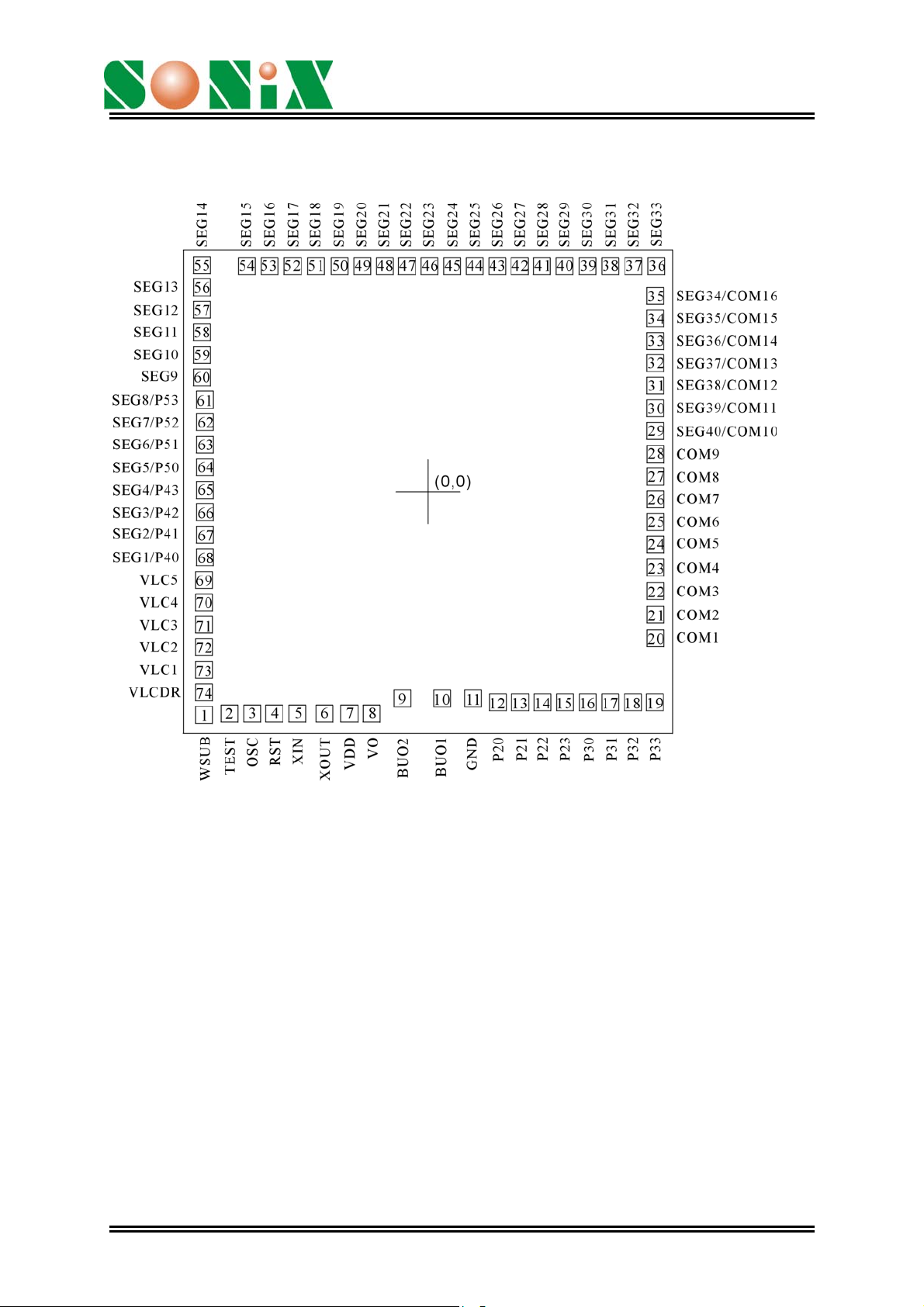
BONDING PAD
SN6A296
LCD Controller with Voice/Dual Tone Melody
SN6A296
Note: The substrate MUST be connected to Vss in PCB layout.
Version: 1.01 September 26, 2002
4
Page 5

SN6A296
LCD Controller with Voice/Dual Tone Melody
DISCLAIMER
The information appearing in SONiX web pages (“this publication”) is believed to be
accurate.
However, this publication could contain technical inaccuracies or typographical errors.
The reader should not assume that this publication is error-free or that it will be
suitable for any particular purpose. SONiXmakes no warranty, express, statutory
implied or by description in this publication or other documents which are referenced
by or linked to this publication. In no event shall SONiX be liable for any special,
incidental, indirect or consequential damages of any kind, or any damages whatsoever,
including, without limitation, those resulting from loss of use, data or profits, whether or
not advised of the possibility of damage, and on any theory of liability, arising out of or
in connection with the use or performance of this publication or other documents which
are referenced by or linked to this publication.
This publication was developed for products offered in Taiwan. SONiX may not offer
the products discussed in this document in other countries. Information is subject to
change without notice. Please contact SONiX or its local representative for
information on offerings available. Integrated circuits sold by SONiX are covered by
the warranty and patent indemnification provisions stipulated in the terms of sale only.
The application circuits illustrated in this document are for reference purposes only.
SONIX DISCLAIMS ALL WARRANTIES, INCLUDING THE WARRANTY OF
MERCHANTABILITY OR FITNESS FOR ANY PURPOSE. SONIX reserves the right
to halt production or alter the specifications and prices, and discontinue marketing the
Products listed at any time without notice. Accordingly, the reader is cautioned to
verify that the data sheets and other information in this publication are current before
placing orders.
Products described herein are intended for use in normal commercial applications.
Applications involving unusual environmental or reliability requirements, e.g. military
equipment or medical life support equipment, are specifically not recommended
without additional processing by SONIX for such application.
Version: 1.01 September 26, 2002
5
 Loading...