

Page 1
SMJ320C31, SMJ320LC31, SMQ320LC31
DIGITAL SIGNAL PROCESSORS
SGUS026B– APRIL 1998 – REVISED APRIL 1999
1
POST OFFICE BOX 1443 • HOUSTON, TEXAS 77251–1443
D
–55°C to 125°C Operating Temperature
Range, QML Processing
D
Processed to MIL-PRF-38535 (QML)
D
SMD Approval for 40- and 50-MHz Versions
D
High-Performance Floating-Point Digital
Signal Processor (DSP):
– SMJ320C31-50 (5 V)
40-ns Instruction Cycle Time
275 Million Operations Per Second
(MOPS), 50 Million Floating-Point
Operations Per Second (MFLOPS),
25 Million Instructions Per Second
(MIPS)
– SMJ320C31-40 (5 V)
50-ns Instruction Cycle Time
220 MOPS, 40 MFLOPS, 20 MIPS
– SMJ320LC31-40 (3.3 V)
50-ns Instruction Cycle Time
220 MOPS, 40 MFLOPS, 20 MIPS
– SMQ320LC31-40 (3.3 V)
50-ns Instruction Cycle Time
220 MOPS, 40 MFLOPS, 20 MIPS
D
32-Bit High-Performance CPU
D
16-/32-Bit Integer and 32-/40-Bit
Floating-Point Operations
D
32-Bit Instruction and Data Words, 24-Bit
Addresses
D
Two 1K Word × 32-Bit Single-Cycle
Dual-Access On-Chip RAM Blocks
D
Boot-Program Loader
D
64-Word × 32-Bit Instruction Cache
D
Eight Extended-Precision Registers
D
T wo Address Generators With Eight
Auxiliary Registers and Two Auxiliary
Register Arithmetic Units (ARAUs)
D
Two Low-Power Modes
D
On-Chip Memory-Mapped Peripherals:
– One Serial Port Supporting
8-/16-/24-/32-Bit Transfers
– Two 32-Bit Timers
– One-Channel Direct Memory Access
(DMA) Coprocessor for Concurrent I/O
and CPU Operation
D
Fabricated Using 0.7 µm Enhanced
Performance Implanted CMOS (EPIC)
Technology by Texas Instruments (TI)
D
Two- and Three-Operand Instructions
D
40 / 32-Bit Floating-Point /Integer Multiplier
and Arithmetic Logic Unit (ALU)
D
Parallel ALU and Multiplier Execution in a
Single Cycle
D
Block-Repeat Capability
D
Zero-Overhead Loops With Single-Cycle
Branches
D
Conditional Calls and Returns
D
Interlocked Instructions for
Multiprocessing Support
D
Bus-Control Registers Configure
Strobe-Control Wait-State Generation
D
Validated Ada Compiler
D
Integer, Floating-Point, and Logical
Operations
D
32-Bit Barrel Shifter
D
One 32-Bit Data Bus (24-Bit Address)
D
Packaging
– 132-Lead Ceramic Quad Flatpack With
Nonconductive Tie-Bar (HFG Suffix)
– 141-Pin Ceramic Staggered Pin
Grid- Array Package (GFA Suffix)
– 132-Lead TAB Frame
– 132-Lead Plastic Quad Flatpack
(PQ Suffix)
description
The SMJ320C31, SMJ320LC31, and SMQ320LC31 digital signal processors (DSPs) are 32-bit, floating-point
processors manufactured in 0.72-µm triple-level-metal CMOS technology. The devices are part of the
SMJ320C3x generation of DSPs from Texas Instruments.
Please be aware that an important notice concerning availability, standard warranty, and use in critical applications of
Texas Instruments semiconductor products and disclaimers thereto appears at the end of this data sheet.
PRODUCTION DATA information is current as of publication date.
Products conform to specifications per the terms of Texas Instruments
standard warranty. Production processing does not necessarily include
testing of all parameters.
EPIC and TI are trademarks of Texas Instruments Incorporated.
Copyright 1999, Texas Instruments Incorporated
On products compliant to MIL-PRF-38535, all parameters are tested
unless otherwise noted. On all other products, production
processing does not necessarily include testing of all parameters.
Page 2

SMJ320C31, SMJ320LC31, SMQ320LC31
DIGITAL SIGNAL PROCESSORS
SGUS026B– APRIL 1998 – REVISED APRIL 1999
2
POST OFFICE BOX 1443 • HOUSTON, TEXAS 77251–1443
description (continued)
The SMJ320C3x internal busing and special digital-signal-processing instruction set have the speed and
flexibility to execute up to 50 MFLOPS. The SMJ320C3x optimizes speed by implementing functions in
hardware that other processors implement through software or microcode. This hardware-intensive approach
provides performance previously unavailable on a single chip.
The SMJ320C3x can perform parallel multiply and ALU operations on integer or floating-point data in a single
cycle. Each processor also possesses a general-purpose register file, a program cache, dedicated ARAUs,
internal dual-access memories, one DMA channel supporting concurrent I/O, and a short machine-cycle time.
High performance and ease of use are results of these features.
General-purpose applications are greatly enhanced by the large address space, multiprocessor interface,
internally and externally generated wait states, one external interface port, two timers, one serial port, and
multiple-interrupt structure. The SMJ320C3x supports a wide variety of system applications from host processor
to dedicated coprocessor.
High-level-language support is easily implemented through a register-based architecture, large address space,
powerful addressing modes, flexible instruction set, and well-supported floating-point arithmetic.
Page 3
SMJ320C31, SMJ320LC31, SMQ320LC31
DIGITAL SIGNAL PROCESSORS
SGUS026B– APRIL 1998 – REVISED APRIL 1999
3
POST OFFICE BOX 1443 • HOUSTON, TEXAS 77251–1443
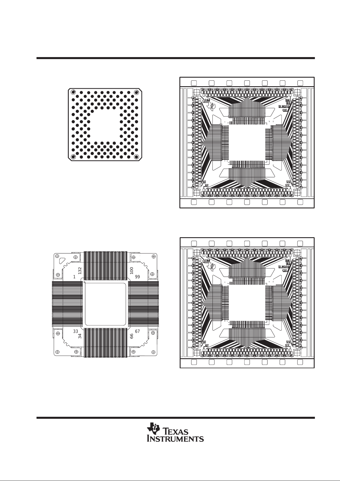
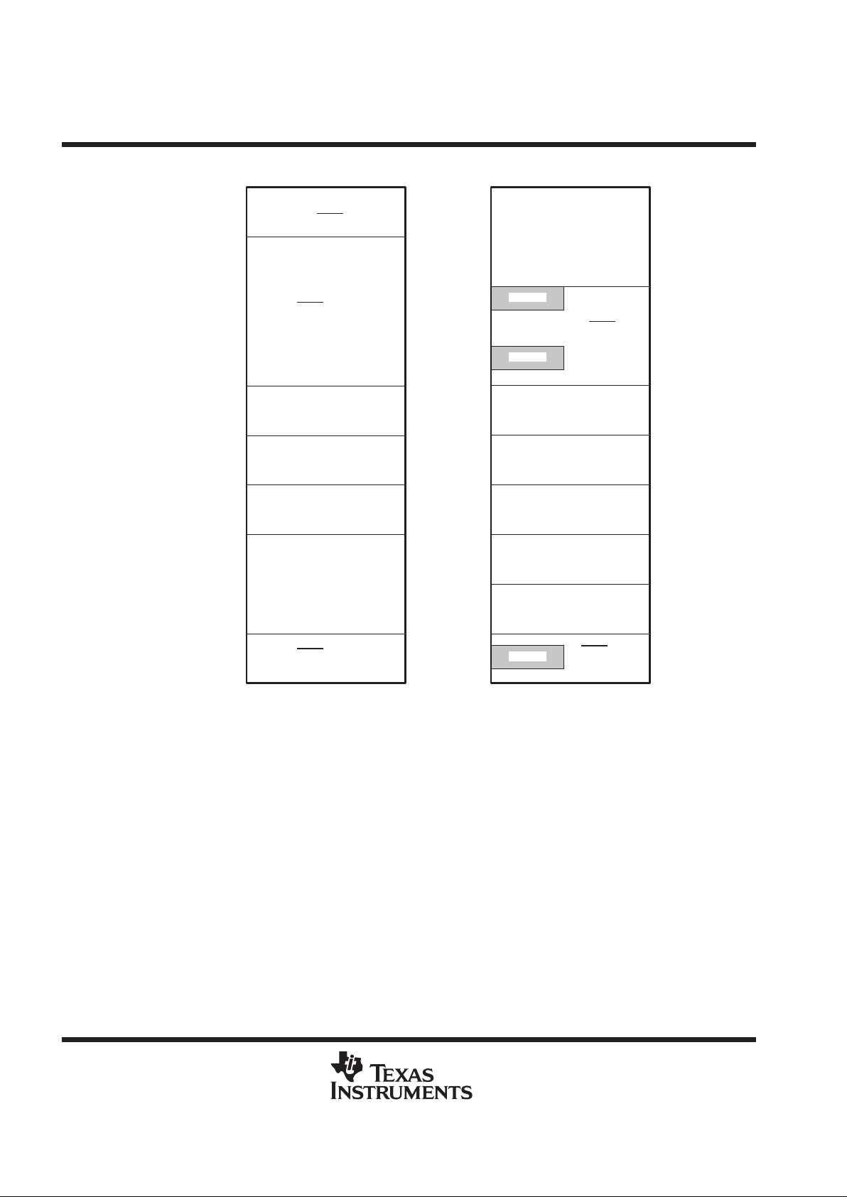
TA PACKAGE
(TOP VIEW)
TB PACKAGE
(TOP VIEW)
Die Face Up
Tab Leads Up
132
1
100
99
66
67
33
34
Die Face Up
Tab Leads Up
100
99
66
67
132
1
33
34
B
18
16
14
12
10
8
6
4
2
19
17
15
13
11
9
7
5
3
1
DFHKMPTV
141-PIN GFA STAGGERED GRID ARRAY
PACKAGE
(BOTTOM VIEW)
ACEGJLNRUW
132-PIN HFG QUAD FLATPACK
(TOP VIEW)
100
991
132
66
34
6733
Page 4
SMJ320C31, SMJ320LC31, SMQ320LC31
DIGITAL SIGNAL PROCESSORS
SGUS026B– APRIL 1998 – REVISED APRIL 1999
4
POST OFFICE BOX 1443 • HOUSTON, TEXAS 77251–1443
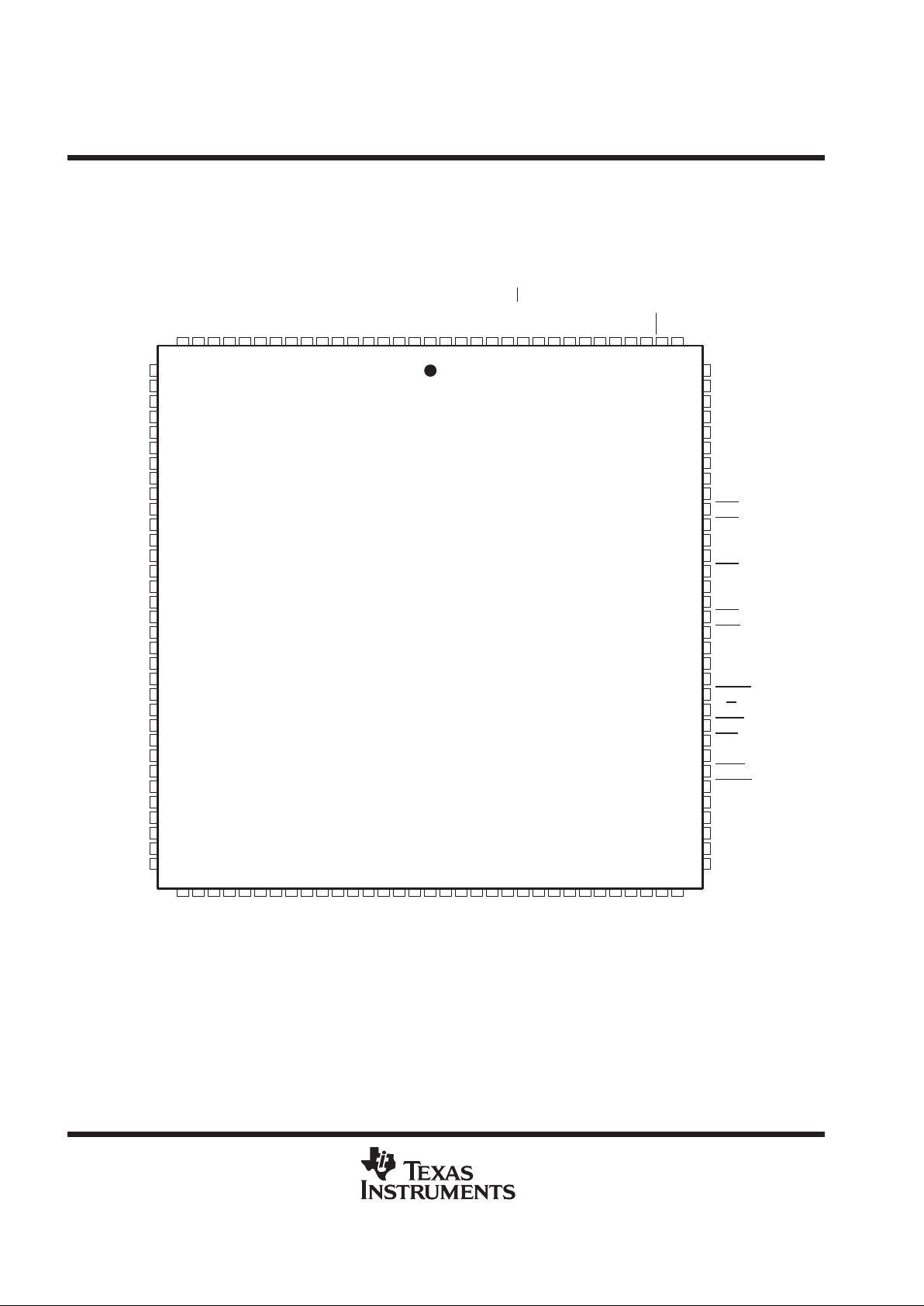
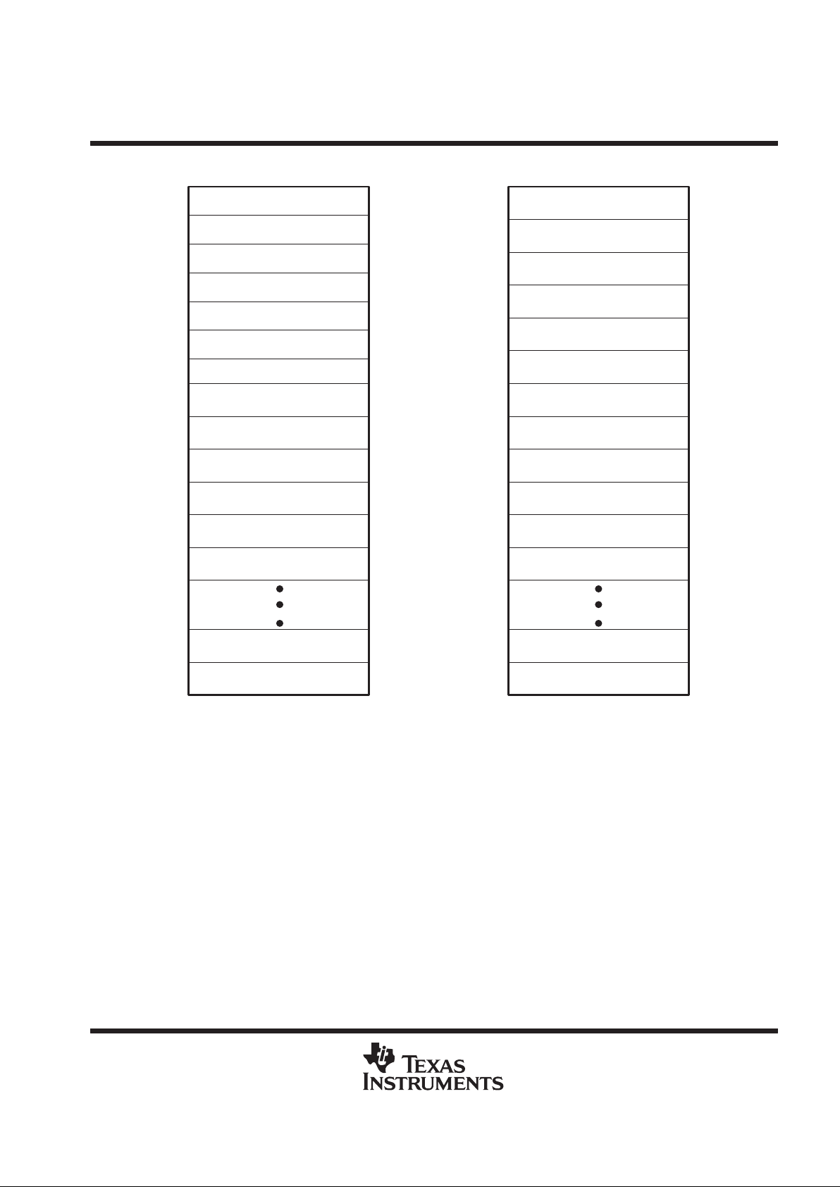
SMQ320LC31 pinout (top view)
The SMQ320LC31 device is also packaged in a132-pin plastic quad flatpack (PQ Suffix). The full part numbers
are SMQ320LC31PQM40 and 5962-9760601NXB.
D0
H1
A7
A5
V
DD
A4
A2
A1
A0
V
SS
D31
V
DD
V
DD
D30
V
SS
V
SS
D29
D28
V
DD
D27
V
SS
D26
D25
D24
D23
D22
D21 V
SS
X2/CLKIN
HOLDA
HOLD
V
DD
RDY
STRB
R/W
RESET
XF0
V
DD
XF1
IACK
INT0
V
SS
V
SS
V
DD
V
DD
INT2
INT3
DR0
V
SS
FSR0
CLKR0
CLKX0
V
SS
FSX0
17 16 15 14 13 12 11 10 9 8 7 6 5 4 3 2 1 132 131 130 129 128 127 126 125 124 123 122 121 120 119 118 117
116
115
114
113
112
111
110
109
108
107
106
105
104
103
102
101
100
99
98
97
96
95
94
93
92
91
90
89
88
87
86
85
84
36
50
49
48
47
46
45
44
43
42
41
40
39
38
37
35
34
33
32
31
30
29
28
27
26
25
24
23
22
21
20
19
18
DD
V
A12
A13
A14
A15
A16
A17
A18
A19
A20
A21
SSVSS
V
51 52 53 54 55 56 57 58 59 60 61 62 63 64 65 66 67 68 69 70 71 72 73 74 75 76 77 78 80 81 82 83
DDVDD
V
A22
A23
MCBL/MP
EMU2
EMU1
EMU0
EMU3
TCLK1
SHZ
DD
V
D18
D16
D15
D14
D13
D12
D11
D9
D10
D7
D6
D5D4D3
DDVDD
V
D8
SS
V
H3
79
A9
V
SS
A6
V
SS
V
DD
D20
A10D19
D2
D1
V
DD
DX0
INT1
X1
SS
V
A11
DD
V
SS
V
TCLK0SSVSSV
V
SS
V
SS
SS
V
D17
SS
V
DD
V
SS
V
SSVSS
V
DD
V
DD
V
PQ PACKAGE
(TOP VIEW)
A8
A3
Page 5
SMJ320C31, SMJ320LC31, SMQ320LC31
DIGITAL SIGNAL PROCESSORS
SGUS026B– APRIL 1998 – REVISED APRIL 1999
5
POST OFFICE BOX 1443 • HOUSTON, TEXAS 77251–1443
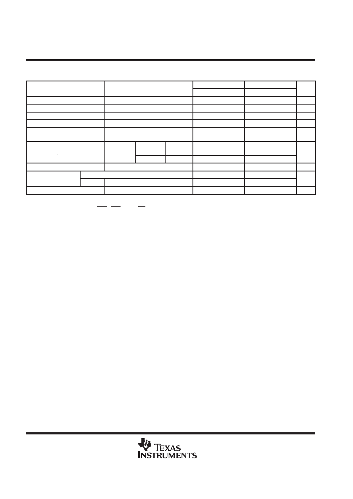
Terminal Assignments
PIN PIN
NUMBER NUMBER
PQ
PKG
HFG
PKG
GFA
PKG
NAME
PQ
PKG
HFG
PKG
GFA
PKG
NAME
29 12 L1 A0 64 47 W9 D10
28 11 K2 A1 63 46 U9 D11
27 10 J1 A2 62 45 V8 D12
26 9 J3 A3 60 43 W7 D13
25 8 G1 A4 58 41 U7 D14
23 6 F2 A5 56 39 V6 D15
22 5 E1 A6 55 38 W5 D16
21 4 E3 A7 54 37 U5 D17
20 3 D2 A8 53 36 V4 D18
18 1 C1 A9 52 35 W3 D19
16 131 C3 A10 50 33 U3 D20
14 129 B2 A11 48 31 V2 D21
13 128 A1 A12 47 30 W1 D22
12 127 C5 A13 46 29 R3 D23
11 126 B4 A14 45 28 T2 D24
10 125 A3 A15 44 27 U1 D25
9 124 C7 A16 43 26 N3 D26
8 123 B6 A17 41 24 P2 D27
7 122 C9 A18 39 22 R1 D28
5 120 B8 A19 38 21 L3 D29
2 117 A7 A20 34 17 M2 D30
1 116 A9 A21 31 14 N1 D31
130 113 B10 A22 108 91 C19 DR0
129 112 A11 A23 116 99 C17 DX0
111 94 E17 CLKR0 124 107 B14 EMU0
112 95 A19 CLKX0 125 108 A13 EMU1
80 63 W19 D0 126 109 B12 EMU2
79 62 V16 D1 123 106 A15 EMU3
78 61 W17 D2 110 93 D18 FSR0
77 60 U13 D3 114 97 B18 FSX0
76 59 V14 D4 81 73 P18 HOLD
75 58 W15 D5 82 72 R19 HOLDA
73 56 U1 1 D6 90 64 V18 H1
72 55 V12 D7 89 65 U17 H3
68 51 W11 D8 99 82 H18 IACK
67 50 V10 D9 100 83 J17 INT0
†
CVSS, V
SSL
, and IVSS are on the same plane.
‡
AVDD, DVDD, CVDD, and PVDD are on the same plane.
§
V
SUBS
connects to die metallization. Tie this pin to clean ground.
Page 6
SMJ320C31, SMJ320LC31, SMQ320LC31
DIGITAL SIGNAL PROCESSORS
SGUS026B– APRIL 1998 – REVISED APRIL 1999
6
POST OFFICE BOX 1443 • HOUSTON, TEXAS 77251–1443
Terminal Assignments (Continued)
PIN PIN
NUMBER NUMBER
PQ
PKG
HFG
PKG
GFA
PKG
NAME
PQ
PKG
HFG
PKG
GFA
PKG
NAME
103 86 E19 INT1 30 18 P4 V
SSL
†
106 89 F18 INT2 35 19 T10 V
SSL
†
107 90 G17 INT3 36 20 K4 DV
SS
127 110 C11 MCBL/MP 37 25 T4 IV
SS
†
92 77 L19 R/W 42 34 G3 DV
SS
95 75 N17 RDY 51 40 K16 CV
SS
†
94 78 K18 RESET 57 44 T8 IV
SS
†
118 101 A17 SHZ 61 52 T12 DV
SS
93 76 M19 STRB 69 53 R11 V
SSL
†
120 103 B16 TCLK0 70 54 J15 V
SSL
†
105 C15 TCLK1 71 67 W13 DV
SS
121 G5 AV
DD
‡
84 68 D10 CV
SS
†
6 130 E7 AV
DD
‡
85 69 D16 IV
SS
†
15 7 E5 AV
DD
‡
86 84 T16 DV
SS
24 15 N5 V
DDL
101 85 D12 V
SSL
†
32 16 R5 V
DDL
102 92 F16 CV
SS
†
33 23 H4 DV
DD
‡
109 96 H16 IV
SS
†
40 32 J5 DV
DD
‡
113 100 D14 V
SUBS
§
49 42 T14 DV
DD
‡
117 102 U15 DV
SS
59 48 R7 V
DDL
119 111 C13 CV
SS
†
65 49 R9 V
DDL
128 71 T18 X1
66 57 R13 DV
DD
‡
88 70 U19 X2/CLKIN
74 66 R15 DV
DD
‡
87 79 J19 XF0
83 74 P16 CV
DD
‡
96 81 G19 XF1
91 80 N15 CV
DD
‡
98 F6 No Connect
97 87 G15 V
DDL
D4 DV
SS
104 88 E15 V
DDL
N19 DV
SS
105 98 L15 PV
DD
‡
R17 DV
SS
115 104 E9 PV
DD
‡
L17 DV
SS
121 114 E13 V
DDL
M16 DV
SS
131 115 E11 V
DDL
D6 DV
SS
132 118 L5 V
SSL
†
A5 DV
SS
3 119 H2 DV
SS
D8 DV
SS
4 132 M4 CV
SS
†
17 2 F4 DV
SS
19 13 T6 CV
SS
†
†
CVSS, V
SSL
, and IVSS are on the same plane.
‡
AVDD, DVDD, CVDD, and PVDD are on the same plane.
§
V
SUBS
connects to die metallization. Tie this pin to clean ground.
Page 7
SMJ320C31, SMJ320LC31, SMQ320LC31
DIGITAL SIGNAL PROCESSORS
SGUS026B– APRIL 1998 – REVISED APRIL 1999
7
POST OFFICE BOX 1443 • HOUSTON, TEXAS 77251–1443
Terminal Functions
TERMINAL
CONDITIONS
NAME QTY
TYPE
†
DESCRIPTION
WHEN
SIGNAL IS Z TYPE
‡
PRIMARY-BUS INTERFACE
D31–D0 32 I/O/Z 32-bit data port S H R
A23–A0 24 O/Z 24-bit address port S H R
R/W 1 O/Z
Read/write. R/W is high when a read is performed and low when a write is performed
over the parallel interface.
S H R
STRB 1 O/Z External-access strobe S H
RDY 1 I
Ready. RDY indicates that the external device is prepared for a transaction
completion.
HOLD 1 I
Hold. When HOLD is a logic low, any ongoing transaction is completed. A23 –A0,
D31–D0, STRB
, and R/W are placed in the high-impedance state and all transac-
tions over the primary-bus interface are held until HOLD
becomes a logic high or until
the NOHOLD bit of the primary-bus-control register is set.
HOLDA 1 O/Z
Hold acknowledge. HOLDA is generated in response to a logic low on HOLD. HOLDA
indicates that A23–A0, D31–D0, STRB, and R/W are in the high-impedance state
and that all transactions over the bus are held. HOLDA
is high in response to a logic
high of HOLD
or the NOHOLD bit of the primary-bus-control register is set.
S
CONTROL SIGNALS
RESET 1 I
Reset. When RESET is a logic low, the device is in the reset condition. When RESET
becomes a logic high, execution begins from the location specified by the reset vector.
INT3–INT0 4 I External interrupts
IACK 1 O/Z
Interrupt acknowledge. IACK is generated by the IACK instruction. IACK can be used
to indicate the beginning or the end of an interrupt-service routine.
S
MCBL/MP 1 I Microcomputer boot-loader/microprocessor mode-select
SHZ 1 I
Shutdown high impedance. When active, SHZ shuts down the device and places all
pins in the high-impedance state. SHZ
is used for board-level testing to ensure that
no dual-drive conditions occur. CAUTION: A low on SHZ
corrupts the device memory
and register contents. Reset the device with SHZ
high to restore it to a known
operating condition.
XF1, XF0 2 I/O/Z
External flags. XF1 and XF0 are used as general-purpose I/Os or to support
interlocked processor instruction.
S R
SERIAL PORT 0 SIGNALS
CLKR0 1 I/O/Z Serial port 0 receive clock. CLKR0 is the serial shift clock for the serial port 0 receiver. S R
CLKX0 1 I/O/Z
Serial port 0 transmit clock. CLKX0 is the serial shift clock for the serial port 0
transmitter.
S R
DR0 1 I/O/Z Data-receive. Serial port 0 receives serial data on DR0. S R
DX0 1 I/O/Z Data-transmit output. Serial port 0 transmits serial data on DX0. S R
FSR0 1 I/O/Z
Frame-synchronization pulse for receive. The FSR0 pulse initiates the data-receive
process using DR0.
S R
FSX0 1 I/O/Z
Frame-synchronization pulse for transmit. The FSX0 pulse initiates the data-transmit
process using DX0.
S R
TIMER SIGNALS
TCLK0 1 I/O/Z
Timer clock 0. As an input, TCLK0 is used by timer 0 to count external pulses. As an
output, TCLK0 outputs pulses generated by timer 0.
S
TCLK1 1 I/O/Z
Timer clock 1. As an input, TCLK0 is used by timer 1 to count external pulses. As an
output, TCLK1 outputs pulses generated by timer 1.
S
†
I = input, O = output, Z = high-impedance state
‡
S = SHZ
active, H = HOLD active, R = RESET active
Page 8
SMJ320C31, SMJ320LC31, SMQ320LC31
DIGITAL SIGNAL PROCESSORS
SGUS026B– APRIL 1998 – REVISED APRIL 1999
8
POST OFFICE BOX 1443 • HOUSTON, TEXAS 77251–1443
Terminal Functions (Continued)
TERMINAL
CONDITIONS
NAME QTY
TYPE
†
DESCRIPTION
WHEN
SIGNAL IS Z TYPE
‡
SUPPLY AND OSCILLATOR SIGNALS
H1 1 O/Z External H1 clock. H1 has a period equal to twice CLKIN. S
H3 1 O/Z External H3 clock. H3 has a period equal to twice CLKIN. S
V
DD
20 I
5-V supply for ’C31 devices and 3.3-V supply for ’LC31 devices. All must be
connected to a common supply plane.
§
V
SS
25 I Ground. All grounds must be connected to a common ground plane.
X1 1 O
Output from the internal-crystal oscillator . If a crystal is not used, X1 should be left
unconnected.
X2/CLKIN 1 I Internal-oscillator input from a crystal or a clock
RESERVED
¶
EMU2–EMU0 3 I Reserved for emulation. Use pullup resistors to V
DD
EMU3 1 O/Z Reserved for emulation S
†
I = input, O = output, Z = high-impedance state
‡
S = SHZ
active, H = HOLD active, R = RESET active
§
Recommended decoupling capacitor value is 0.1 µF.
¶
Follow the connections specified for the reserved pins. Use 18-kΩ–22-kΩ pullup resistors for best results. All VDD supply pins must be connected
to a common supply plane, and all ground pins must be connected to a common ground plane.
Page 9
SMJ320C31, SMJ320LC31, SMQ320LC31
DIGITAL SIGNAL PROCESSORS
SGUS026B– APRIL 1998 – REVISED APRIL 1999
9
POST OFFICE BOX 1443 • HOUSTON, TEXAS 77251–1443
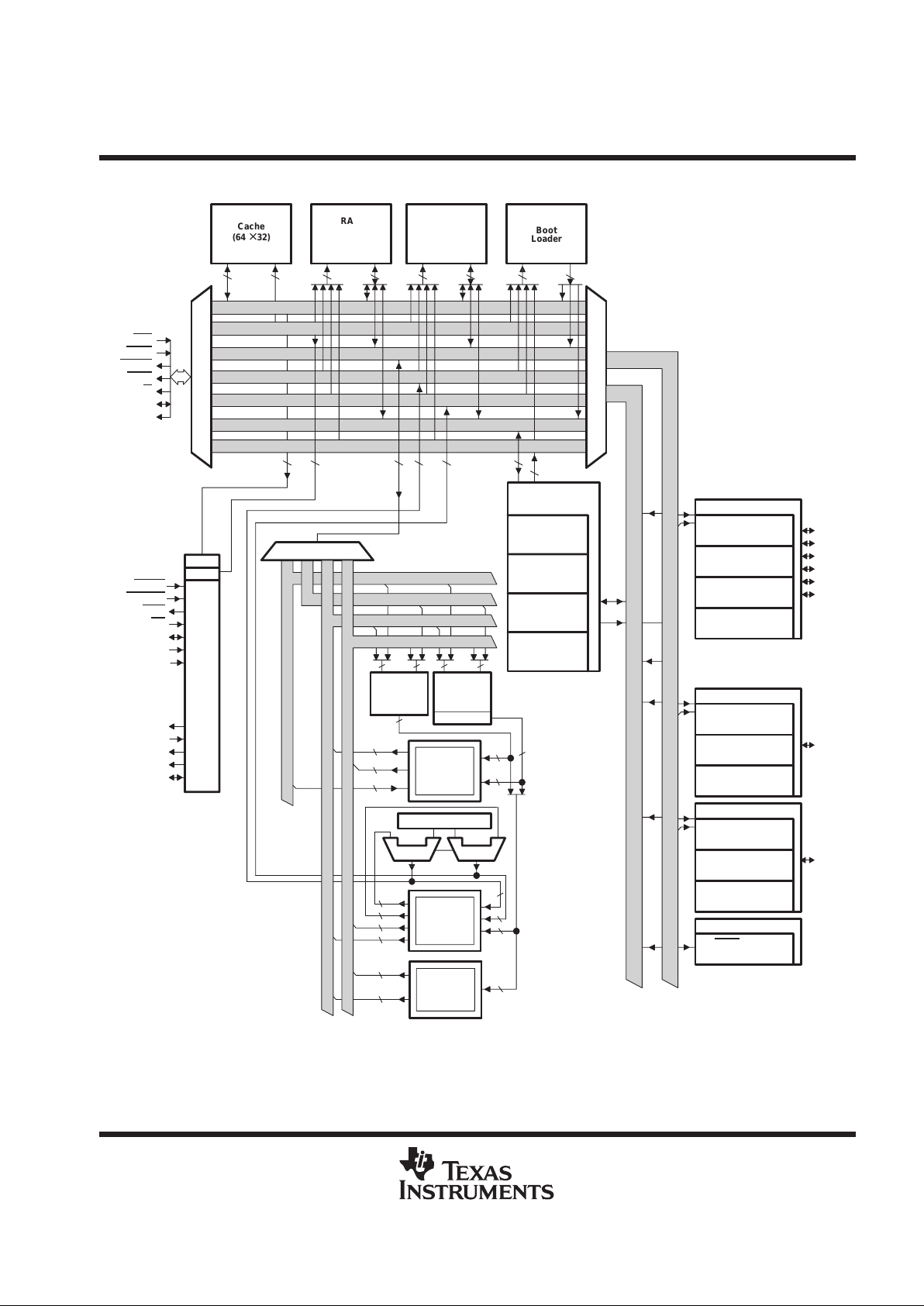
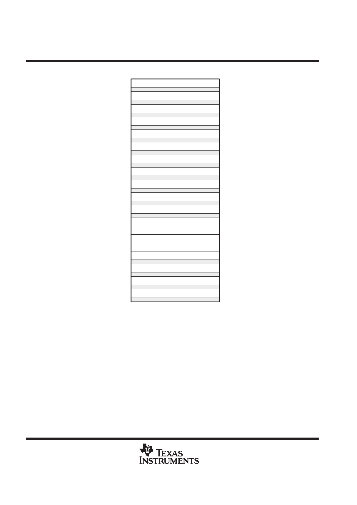
functional block diagram
24
Boot
Loader
Cache
(64
× 32)
RAM
Block 0
(1K
× 32)
RAM
Block 1
(1K × 32)
RDY
HOLD
HOLDA
STRB
R/W
D31–D0
A23–A0
RESET
IR
PC
CPU1
REG1
REG2
MUX
40
32
32
32
32
32
32
32
24
24
24
24
BK
ARAU0 ARAU1
DISP0, IR0, IR1
Extended-
Precision
Registers
(R7–R0)
Auxiliary
Registers
(AR0–AR7)
Other
Registers
(12)
40
40
40
40
Multiplier
32-Bit
Barrel
Shifter
ALU
DMA Controller
Global-Control
Register
Source-Address
Register
Destination-
Address
Register
Serial Port 0
Serial-Port-Control
Register
Receive/Transmit
(R/X) Timer Register
Data-Transmit
Register
Data-Receive
Register
FSX0
DX0
CLKX0
FSR0
DR0
CLKR0
Timer 0
Global-Control
Register
Timer-Period
Register
Timer-Counter
Register
TCLK0
Timer 1
Global-Control
Register
Timer-Period
Register
Timer-Counter
Register
TCLK1
Port Control
STRB
-Control
Register
Transfer-
Counter
Register
PDATA Bus
PADDR Bus
DDATA Bus
DADDR1 Bus
DADDR2 Bus
DMADATA Bus
DMAADDR Bus
24
40
32
32
24
24
32
INT(3–0)
IACK
MCBL/MP
XF(1,0)
VDD(19–0)
VSS(24–0)
X1
X2/CLKIN
H1
H3
EMU(3–0)
32 24 24
24 2432 32 32
CPU2
32 32 40 40
MUX
Controller
Peripheral Data Bus
Peripheral Address Bus
CPU1
REG1
REG2
MUX
Page 10
SMJ320C31, SMJ320LC31, SMQ320LC31
DIGITAL SIGNAL PROCESSORS
SGUS026B– APRIL 1998 – REVISED APRIL 1999
10
POST OFFICE BOX 1443 • HOUSTON, TEXAS 77251–1443
memory map
†
Peripheral Bus
Memory-Mapped Registers
(6K Words Internal)
Reset, Interrupt, Trap V ector, and
Reserved Locations (64)
(External STRB
Active)
0h
03Fh
040h
External
STRB
Active
(8M Words – 64 Words)
7FFFFFh
Reserved
(32K Words)
800000h
807FFFh
808000h
8097FFh
RAM Block 0
(1K Words Internal)
809800h
809BFFh
809C00h
809FFFh
80A000h
External
STRB
Active
(8M Words – 40K Words)
FFFFFFh
0h
FFFh
1000h
7FFFFFh
Reserved
(32K Words)
800000h
807FFFh
Peripheral Bus
Memory-Mapped Registers
(6K Words Internal)
808000h
8097FFh
RAM Block 0
(1K Words Internal)
809800h
809BFFh
809C00h
809FFFh
80A000h
External
STRB
Active
(8M Words –
40K Words)
FFFFFFh
Boot 1
Boot 2
400000h
RAM Block 1
(1K Words – 63 Words Internal)
809FC0h
809FC1h
User-Program Interrupt
and Trap Branches
(63 Words Internal)
Boot 3
FFF000h
External
STRB
Active
(8M Words –
4K Words)
Reserved for Boot-Loader
Operations
(a) Microprocessor Mode
(b) Microcomputer/Boot-Loader Mode
RAM Block 1
(1K Words Internal)
†
Figure 1 depicts the memory map for the SMJ320C31. See the
TMS320C3x Users Guide
(literature number SPRU031) for a detailed description
of this memory mapping.
Figure 1. SMJ320C31 Memory Map
Page 11
SMJ320C31, SMJ320LC31, SMQ320LC31
DIGITAL SIGNAL PROCESSORS
SGUS026B– APRIL 1998 – REVISED APRIL 1999
11
POST OFFICE BOX 1443 • HOUSTON, TEXAS 77251–1443
memory map (continued)
TINT0
Reserved
TINT0
TINT1
DINT
Reserved
TRAP 0
TRAP 27
Reserved
Reset
00h
INT0
809FC1h
INT1
01h
INT1
809FC2h
INT2
02h
INT2
809FC3h
INT3
03h
INT3
809FC4h
XINT0
04h
XINT0
809FC5h
RINT0
06h
RINT0
809FC6h
07h
Reserved
809FC7h
809FC8h
08h
09h
809FC9h
0Ah
TINT1
809FCAh
0Bh
DINT
809FCBh
0Ch
Reserved
809FDFh
1Fh
809FCCh
20h TRAP 0
809FE0h
3Bh TRAP 27809FFBh
3Ch
Reserved
809FFFh
3Fh
809FFCh
(a) Microprocessor Mode (b) Microcomputer/Boot-Loader Mode
INT0
05h
Figure 2. Reset, Interrupt, and Trap Vector/Branches Memory-Map Locations
Page 12
SMJ320C31, SMJ320LC31, SMQ320LC31
DIGITAL SIGNAL PROCESSORS
SGUS026B– APRIL 1998 – REVISED APRIL 1999
12
POST OFFICE BOX 1443 • HOUSTON, TEXAS 77251–1443
memory map (continued)
FSX/DX/CLKX Serial Port Control
FSR/DR/CLKR Serial Port Control
Serial R/X Timer Control
Serial R/X Timer Counter
Serial R/X Timer Period Register
Data-Transmit
Data-Receive
Primary-Bus Control
DMA Global Control
DMA Source Address
DMA Destination Address
DMA Transfer Counter
Timer 0 Global Control
Timer 0 Counter
Timer 0 Period Register
Timer 1 Global Control
Timer 1 Counter
Timer 1 Period Register
Serial Global Control
808000h
808004h
808006h
808008h
808020h
808024h
808028h
808030h
808034h
808038h
808040h
808042h
808043h
808044h
808045h
808046h
808048h
80804Ch
808064h
†
Shading denotes reserved address locations
Figure 3. Peripheral Bus Memory-Mapped Registers
†
Page 13
SMJ320C31, SMJ320LC31, SMQ320LC31
DIGITAL SIGNAL PROCESSORS
SGUS026B– APRIL 1998 – REVISED APRIL 1999
13
POST OFFICE BOX 1443 • HOUSTON, TEXAS 77251–1443
absolute maximum ratings over specified temperature range (unless otherwise noted)
†
’C31 ’LC31
Supply voltage, V
DD
(see Note 1) –0.3 V to 7 V. . . . . . . . . . . . . . . . . . . . . . . . . . . . . . –0.3 V to 5 V. . . . . . . . . .
Input voltage, V
I
–0.3 V to 7 V. . . . . . . . . . . . . . . . . . . . . . . . . . . . . . . . . . . . . . . . . . . . . –0.3 V to 5 V. . . . . . . . . .
Output voltage, V
O
–0.3 V to 7 V. . . . . . . . . . . . . . . . . . . . . . . . . . . . . . . . . . . . . . . . . . . –0.3 V to 5 V. . . . . . . . . .
Continuous power dissipation (worst case) (see Note 2) 1.7 W. . . . . . . . . . . . . . . . . .
(for SMJ320C31-33)
850 mW. . . . . . . . . . . . . .
(for SMJ320LC31-33)
Operating free-air temperature, T
A
–55°C to 125°C. . . . . . . . . . . . . . . . . . . . . . . . . . . . – –55°C to 125°C. . . . . .
Storage temperature, T
stg
– 65°C to 150°C. . . . . . . . . . . . . . . . . . . . . . . . . . . . . . . . . . . – 65°C to 150°C. . . . . . .
†
Stresses beyond those listed under “absolute maximum ratings” may cause permanent damage to the device. These are stress ratings only, and
functional operation of the device at these or any other conditions beyond those indicated under “recommended operating conditions” is not
implied. Exposure to absolute-maximum-rated conditions for extended periods may affect device reliability.
NOTES: 1. All voltage values are with respect to VSS.
2. Actual operating power is less. This value was obtained under specially produced worst-case test conditions for the TMS320C31-33
and the TMS320LC31-33, which are not sustained during normal device operation. These conditions consist of continuous parallel
writes of a checkerboard pattern to both primary and extension buses at the maximum rate possible. See normal (ICC) current
specification in the electrical characteristics table and also read
Calculation of TMS320C30 Power Dissipation Application Report
(literature number SPRA020)
.
recommended operating conditions (see Note 3)
’C31 ’LC31
MIN NOM MAX MIN NOM MAX
UNIT
V
DD
Supply voltage (DVDD, etc.)
’320C31-40
’320C31-50
’320LC31-40
4.75
4.75
5
5
5.25
5.25
3.13 3.3 3.47
V
V
SS
Supply voltage (CVSS, etc.) 0 0 V
High-level input voltage (except RESET) 2.1 VDD+ 0.3* 1.8 VDD+ 0.3* V
V
IH
High-level input voltage (RESET) 2.2 VDD+ 0.3* 2.2 VDD+ 0.3* V
V
IL
Low-level input voltage – 0.3* 0.8 – 0.3* 0.6 V
I
OH
High-level output current – 300 – 300 µA
I
OL
Low-level output current 2 2 mA
T
A
Operating free-air temperature –55 125 –55 125 °C
V
TH
High-level input voltage for CLKIN 3.0 VDD+ 0.3* 2.5 VDD+ 0.3* V
* This parameter is not production tested.
NOTE 3: All voltage values are with respect to VSS. All input and output voltage levels are TTL-compatible. CLKIN can be driven by a CMOS
clock.
Page 14
SMJ320C31, SMJ320LC31, SMQ320LC31
DIGITAL SIGNAL PROCESSORS
SGUS026B– APRIL 1998 – REVISED APRIL 1999
14
POST OFFICE BOX 1443 • HOUSTON, TEXAS 77251–1443
electrical characteristics over recommended ranges of supply voltage (unless otherwise noted)
(see Note 3)
†
’C31 ’LC31
PARAMETER
TEST CONDITIONS
MIN TYP‡MAX MIN TYP‡MAX
UNIT
V
OH
High-level output voltage VDD = MIN, IOH = MAX 2.4 3 2 V
V
OL
Low-level output voltage VDD = MIN, IOH = MAX 0.3 0.6 0.4 V
I
Z
High-impedance current VDD = MAX – 20 + 20 – 20 + 20 µA
I
I
Input current VI = VSS to V
DD
– 10 + 10 – 10 + 10 µA
I
IP
Input current (with internal
pullup)
Inputs with internal pullups
§
– 600 20 – 600 10 µA
I
Supply current
¶#
TA = 25°C,
fx = 40 MHz
’C31-40
’LC31-40
160 400 150 300
mA
CC
y
V
DD
=
MAX
fx = 50 MHz ’C31-50 200 425
I
DD
Supply current Standby, IDLE2 Clocks shut off 50 20 µA
Input
All inputs except CLKIN 15* 15*
p
C
i
capacitance
CLKIN
25 25
pF
C
o
Output capacitance 20* 20* pF
†
All input and output voltage levels are TTL compatible.
‡
For ’C31, all typical values are at VDD = 5 V, TA = 25°C. For ’LC31, all typical values are at VDD = 3.3 V, TA = 25°C.
§
Pins with internal pullup devices: INT3
–INT0, MCBL/MP.
¶
Actual operating current is less than this maximum value. This value was obtained under specially produced worst-case test conditions, which
are not sustained during normal device operation. These conditions consist of continuous parallel writes of a checkerboard pattern to both primary
and expansion buses at the maximum rate possible. See
Calculation of TMS320C30 Power Dissipation Application Report
(literature number
SPRA020).
#
fx is the input clock frequency.
* This parameter is not production tested.
NOTE 3: All voltage values are with respect to VSS. All input and output voltage levels are TTL-compatible. CLKIN can be driven by a CMOS
clock.
Page 15
SMJ320C31, SMJ320LC31, SMQ320LC31
DIGITAL SIGNAL PROCESSORS
SGUS026B– APRIL 1998 – REVISED APRIL 1999
15
POST OFFICE BOX 1443 • HOUSTON, TEXAS 77251–1443
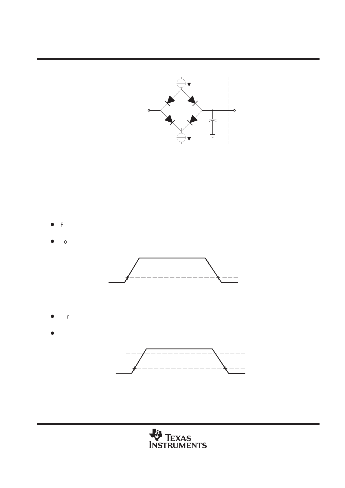
PARAMETER MEASUREMENT INFORMATION
Tester Pin
Electronics
V
Load
I
OL
C
T
I
OH
Output
Under
Test
Where: I
OL
= 2 mA (all outputs)
I
OH
= 300 µA (all outputs)
V
LOAD
= Selected to emulate 50-Ω termination (typical value = 1.54 V).
C
T
= 80-pF typical load-circuit capacitance
Figure 4. SMJ320C31 Test Load Circuit
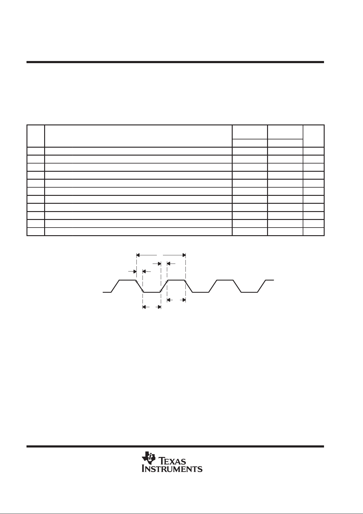
signal transition levels for ’C31 (see Figure 5 and Figure 6)
TTL-level outputs are driven to a minimum logic-high level of 2.4 V and to a maximum logic-low level of 0.6 V .
Output transition times are specified as follows:
D
For a high-to-low transition on a TTL-compatible output signal, the level at which the output is said to be
no longer high is 2 V and the level at which the output is said to be low is 1 V.
D
For a low-to-high transition, the level at which the output is said to be no longer low is 1 V and the level at
which the output is said to be high is 2 V.
0.6 V
1 V
2 V
2.4 V
Figure 5. TTL-Level Outputs
Transition times for TTL-compatible inputs are specified as follows:
D
For a high-to-low transition on an input signal, the level at which the input is said to be no longer high is
2.1 V and the level at which the input is said to be low is 0.8 V.
D
For a low-to-high transition on an input signal, the level at which the input is said to be no longer low is
0.8 V and the level at which the input is said to be high is 2.1 V.
0.8 V
2.1 V
Figure 6. TTL-Level Inputs
Page 16
SMJ320C31, SMJ320LC31, SMQ320LC31
DIGITAL SIGNAL PROCESSORS
SGUS026B– APRIL 1998 – REVISED APRIL 1999
16
POST OFFICE BOX 1443 • HOUSTON, TEXAS 77251–1443
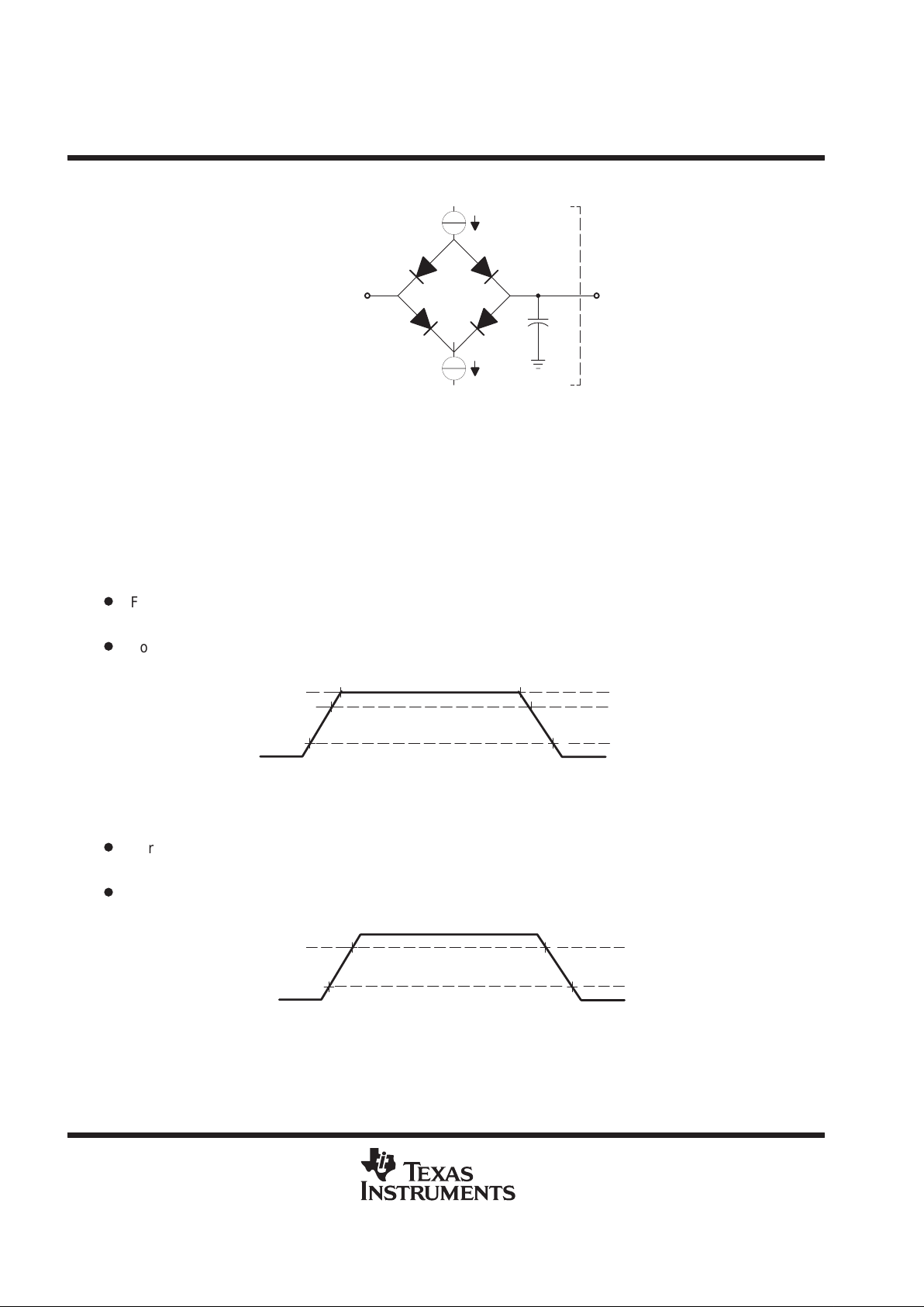
PARAMETER MEASUREMENT INFORMATION
Tester Pin
Electronics
V
Load
I
OL
C
T
I
OH
Output
Under
Test
Where: I
OL
= 2 mA (all outputs)
I
OH
= 300 µA (all outputs)
V
LOAD
= 2.15 V
C
T
= 80-pF typical load-circuit capacitance
Figure 7. SMJ320LC31 Test Load Circuit
signal transition levels for ’LC31 (see Figure 8 and Figure 9)
Outputs are driven to a minimum logic-high level of 2 V and to a maximum logic-low level of 0.4 V. Output
transition times are specified as follows:
D
For a high-to-low transition on an output signal, the level at which the output is said to be no longer high
is 2 V and the level at which the output is said to be low is 1 V.
D
For a low-to-high transition, the level at which the output is said to be no longer low is 1 V and the level at
which the output is said to be high is 2 V.
0.4 V
0.6 V
2 V
1.8 V
Figure 8. ’LC31 Output Levels
Transition times for inputs are specified as follows:
D
For a high-to-low transition on an input signal, the level at which the input is said to be no longer high is
1.8 V and the level at which the input is said to be low is 0.6 V.
D
For a low-to-high transition on an input signal, the level at which the input is said to be no longer low is
0.6 V and the level at which the input is said to be high is 1.8 V.
0.6 V
1.8 V
Figure 9. ’LC31 Input Levels
Page 17
SMJ320C31, SMJ320LC31, SMQ320LC31
DIGITAL SIGNAL PROCESSORS
SGUS026B– APRIL 1998 – REVISED APRIL 1999
17
POST OFFICE BOX 1443 • HOUSTON, TEXAS 77251–1443
PARAMETER MEASUREMENT INFORMATION
timing parameter symbology
Timing parameter symbols used herein were created in accordance with JEDEC Standard 100-A. In order to
shorten the symbols, some of the pin names and other related terminology have been abbreviated as follows,
unless otherwise noted:
A A23–A0 H H1 and H3
ASYNCH Asynchronous reset signals HOLD HOLD
C CLKX0 HOLDA HOLDA
CI CLKIN IACK IACK
CLKR CLKR0 INT INT3–INT0
CONTROL Control signals RDY RDY
D D31–D0 R W R/W
DR DR RESET RESET
DX DX S STRB
FS FSX/R SCK CLKX/R
FSX FSX0 SHZ SHZ
FSR FSR0 TCLK TCLK0, TCLK1, or TCLKx
GPI General-purpose input XF XF0, XF1, or XFx
GPIO General-purpose input/output; peripheral pin XFIO XFx switching from input to output
GPO General-purpose output
Page 18
SMJ320C31, SMJ320LC31, SMQ320LC31
DIGITAL SIGNAL PROCESSORS
SGUS026B– APRIL 1998 – REVISED APRIL 1999
18
POST OFFICE BOX 1443 • HOUSTON, TEXAS 77251–1443
timing
Timing specifications apply to the SMJ320C31 and SMJ320LC31.
X2/CLKIN, H1, and H3 timing
The following table defines the timing parameters for the X2/CLKIN, H1, and H3 interface signals.
timing parameters for X2/CLKIN, H1, H3 (see Figure 10, Figure 11, Figure 12, and Figure 13)
NO.
’C31-40
’LC31-40
’C31-50
UNIT
MIN MAX MIN MAX
1 t
f(CI)
Fall time, CLKIN 5* 5* ns
2 t
w(CIL)
Pulse duration, CLKIN low t
c(CI)
= min 9 7 ns
3 t
w(CIH)
Pulse duration, CLKIN high t
c(CI)
= min 9 7 ns
4 t
r(CI)
Rise time, CLKIN 5* 5* ns
5 t
c(CI)
Cycle time, CLKIN 25 303 20 303 ns
6 t
f(H)
Fall time, H1 and H3 3 3 ns
7 t
w(HL)
Pulse duration, H1 and H3 low P–5
†
P–5
†
ns
8 t
w(HH)
Pulse duration, H1 and H3 high P–6
†
P–6
†
ns
9 t
r(H)
Rise time, H1 and H3 3 3 ns
10 t
d(HL-HH)
Delay time. from H1 low to H3 high or from H3 low to H1 high 0 4 0 4 ns
11 t
c(H)
Cycle time, H1 and H3 50 606 40 606 ns
†
P = t
c(CI)
* This parameter is not production tested.
1
4
X2/CLKIN
3
5
2
Figure 10. Timing for X2/CLKIN
Page 19

SMJ320C31, SMJ320LC31, SMQ320LC31
DIGITAL SIGNAL PROCESSORS
SGUS026B– APRIL 1998 – REVISED APRIL 1999
19
POST OFFICE BOX 1443 • HOUSTON, TEXAS 77251–1443
X2/CLKIN, H1, and H3 timing (continued)
H3
H1
6
9
10
10
6
9
11
7
8
7
8
11
Figure 11. Timing for H1 and H3
0.00
1.00
2.00
3.00
4.00
5.00
6.00
7.00
8.00
–60.00 –40.00 –20.00 0.00 20.00 40.00 60.00 80.00 100.00 120.00 140.00
Temperature
CLKIN to H1/H3 - ns
4.5 V Band
5.5 V Band
0
1
2
3
4
5
6
7
8
Figure 12. SMJ320C31 CLKIN to H1/H3 as a Function of Temperature
(Typical)
Page 20

SMJ320C31, SMJ320LC31, SMQ320LC31
DIGITAL SIGNAL PROCESSORS
SGUS026B– APRIL 1998 – REVISED APRIL 1999
20
POST OFFICE BOX 1443 • HOUSTON, TEXAS 77251–1443
X2/CLKIN, H1, and H3 timing (continued)
0.00
2.00
4.00
6.00
8.00
10.00
12.00
–60.00 –40.00 –20.00 0.00 20.00 40.00 60.00 80.00 100.00 120.00 140.00
Temperature
CLKIN to H1/H3 - ns
2.5 V Band
3.8 V Band
0
2
4
6
8
10
12
Figure 13. SMJ320LC31 CLKIN to H1/H3 as a Function of Temperature
(Typical)
Page 21

SMJ320C31, SMJ320LC31, SMQ320LC31
DIGITAL SIGNAL PROCESSORS
SGUS026B– APRIL 1998 – REVISED APRIL 1999
21
POST OFFICE BOX 1443 • HOUSTON, TEXAS 77251–1443
memory read/write timing
The following table defines memory read/write timing parameters for STRB
.
timing parameters for memory (STRB = 0) read/write (see Figure 14 and Figure 15)
†
NO.
’C31-40
’LC31-40
’C31-50
UNIT
MIN MAX MIN MAX
12 t
d(H1L-SL)
Delay time, H1 low to STRB low 0* 6 0* 5 ns
13 t
d(H1L-SH)
Delay time, H1 low to STRB high 0* 6 0* 5 ns
14 t
d(H1H-RWL)R
Delay time, H1 high to R/W low (read) 0* 9 0* 7 ns
15 t
d(H1L-A)
Delay time, H1 low to A valid 0* 10 0* 10 ns
16 t
su(D-H1L)R
Setup time, D before H1 low (read) 14 10 ns
17 t
h(H1L-D)R
Hold time, D after H1 low (read) 0 0 ns
18 t
su(RDY -H1H)
Setup time, RDY before H1 high 8 6 ns
19 t
h(H1H-RDY)
Hold time, RDY after H1 high 0 0 ns
20 t
d(H1H-RWH)W
Delay time, H1 high to R/W high (write) 9 7 ns
21 t
v(H1L-D)W
Valid time, D after H1 low (write) 17 14 ns
22 t
h(H1H-D)W
Hold time, D after H1 high (write) 0 0 ns
23 t
d(H1H-A)W
Delay time, H1 high to A valid on back-to-back write cycles (write) 15 14 ns
24 t
d(A-RDY)
Delay time, RDY from A valid 7* 6* ns
†
See Figure 16 for address bus timing variation with load capacitance greater than typical load-circuit capacitance (CT = 80 pF).
* This parameter is not production tested.
12
14
15
13
16
17
19
18
H3
H1
R/W
A
D
RDY
STRB
24
NOTE A: STRB remains low during back-to-back read operations.
Figure 14. Timing for Memory (STRB = 0) Read
Page 22

SMJ320C31, SMJ320LC31, SMQ320LC31
DIGITAL SIGNAL PROCESSORS
SGUS026B– APRIL 1998 – REVISED APRIL 1999
22
POST OFFICE BOX 1443 • HOUSTON, TEXAS 77251–1443
memory read/write timing (continued)
14
12
RDY
D
A
R/W
STRB
H1
H3
20
22
23
18
19
21
15
13
Figure 15. Timing for Memory (STRB = 0) Write
4.00
3.50
3.00
2.50
2.00
1.50
1.00
0.50
10 15 20 25 30 35 40 45 50 55 60 65 70 75 80 85 90 95 100
Change in Load Capacitance, pF
Change in Address-Bus Timing, ns
Address-Bus Timing Variation Load Capacitance
NOTE A: 30 pF/ns slope
Figure 16. Address-Bus Timing Variation With Load Capacitance (see Note A)
Page 23

SMJ320C31, SMJ320LC31, SMQ320LC31
DIGITAL SIGNAL PROCESSORS
SGUS026B– APRIL 1998 – REVISED APRIL 1999
23
POST OFFICE BOX 1443 • HOUSTON, TEXAS 77251–1443
XF0 and XF1 timing when executing LDFI or LDII
The following table defines the timing parameters for XF0 and XF1 during execution of LDFI or LDII.
timing for XF0 and XF1 when executing LDFI or LDII for SMJ320C31 (see Figure 17)
’C31-40 ’LC31-40 ’C31-50
NO
.
MIN MAX MIN MAX MIN MAX
UNIT
25 t
d(H3H-XF0L)
Delay time, H3 high to XF0 low 13 13 12 ns
26 t
su(XF1-H1L)
Setup time, XF1 before H1 low 9 10 8 ns
27 t
h(H1L-XF1)
Hold time, XF1 after H1 low 0 0 0 ns
H3
H1
STRB
R/W
A
D
RDY
XF0 Pin
XF1 Pin
Fetch
LDFI or LDII
Decode Read Execute
25
26
27
Figure 17. Timing for XF0 and XF1 When Executing LDFI or LDII
Page 24

SMJ320C31, SMJ320LC31, SMQ320LC31
DIGITAL SIGNAL PROCESSORS
SGUS026B– APRIL 1998 – REVISED APRIL 1999
24
POST OFFICE BOX 1443 • HOUSTON, TEXAS 77251–1443
XF0 timing when executing STFI and STII
†
The following table defines the timing parameters for the XF0 pin during execution of STFI or STII.
timing for XF0 when executing STFI or STII (see Figure 18)
NO.
’C31-40
’LC31-40
’C31-50
UNIT
MIN MAX MIN MAX
28 t
d(H3H-XF0H)
Delay time, H3 high to XF0 high 13 12 ns
†
XF0 is always set high at the beginning of the execute phase of the interlock-store instruction. When no pipeline conflicts occur, the address of
the store is also driven at the beginning of the execute phase of the interlock-store instruction. However, if a pipeline conflict prevents the store
from executing, the address of the store will not be driven until the store can execute.
H3
H1
STRB
R/W
A
D
RDY
XF0 Pin
Fetch
STFI or STII Read Execute
28
Decode
Figure 18. Timing for XF0 When Executing an STFI or STII
Page 25

SMJ320C31, SMJ320LC31, SMQ320LC31
DIGITAL SIGNAL PROCESSORS
SGUS026B– APRIL 1998 – REVISED APRIL 1999
25
POST OFFICE BOX 1443 • HOUSTON, TEXAS 77251–1443
XF0 and XF1 timing when executing SIGI
The following table defines the timing parameters for the XF0 and XF1 pins during execution of SIGI.
timing for XF0 and XF1 when executing SIGI for SMJ320C31 (see Figure 19)
’C31-40 ’LC31-40 ’C31-50
NO
.
MIN MAX MIN MAX MIN MAX
UNIT
29 t
d(H3H-XF0L)
Delay time, H3 high to XF0 low 13 13 12 ns
30 t
d(H3H-XF0H)
Delay time, H3 high to XF0 high 13 13 12 ns
31 t
su(XF1-H1L)
Setup time, XF1 before H1 low 9 10 8 ns
32 t
h(H1L-XF1)
Hold time, XF1 after H1 low 0 0 0 ns
H3
H1
Fetch
SIGI Decode Read Execute
XF0
XF1
31
32
29
30
Figure 19. Timing for XF0 and XF1 When Executing SIGI
Page 26

SMJ320C31, SMJ320LC31, SMQ320LC31
DIGITAL SIGNAL PROCESSORS
SGUS026B– APRIL 1998 – REVISED APRIL 1999
26
POST OFFICE BOX 1443 • HOUSTON, TEXAS 77251–1443
loading when XF is configured as an output
The following table defines the timing parameter for loading the XF register when the XFx pin is configured as
an output.
timing for loading the XF register when configured as an output pin (see Figure 20)
NO.
’C31-40
’LC31-40
’C31-50
UNIT
MIN MAX MIN MAX
33 t
v(H3H-XF)
Valid time, H3 high to XFx 13 12 ns
Fetch Load
Decode Read Execute
H3
H1
OUTXFx Bit
(see Note A)
XFx Pin
1 or 0
33
Instruction
NOTE A: OUTXFx represents either bit 2 or 6 of the IOF register.
Figure 20. Timing for Loading XF Register When Configured as an Output Pin
Page 27

SMJ320C31, SMJ320LC31, SMQ320LC31
DIGITAL SIGNAL PROCESSORS
SGUS026B– APRIL 1998 – REVISED APRIL 1999
27
POST OFFICE BOX 1443 • HOUSTON, TEXAS 77251–1443
changing XFx from an output to an input
The following table defines the timing parameters for changing the XFx pin from an output pin to an input pin.
timing of XFx changing from output to input mode for SMJ320C31 (see Figure 21)
’C31-40 ’LC31-40 ’C31-50
NO
.
MIN MAX MIN MAX MIN MAX
UNIT
34 t
h(H3H-XF)
Hold time, XFx after H3 high 13* 13* 12* ns
35 t
su(XF-H1L)
Setup time, XFx before H1 low 9 10 8 ns
36 t
h(H1L-XF)
Hold time, XFx after H1 low 0 0 0 ns
* This parameter is not production tested.
Execute
Load of IOF
Buffers Go
From Output
to Output
Synchronizer
Delay
Value on Pin
Seen in IOF
H3
H1
XFx Pin
INXFx Bit
(see Note A)
I
/OxFx Bit
(see Note A)
34
35
36
Data
Sampled
Data
Seen
Output
NOTE A: I/OxFx represents either bit 1 or bit 5 of the IOF register, and INXFx represents either bit 3 or bit 7 of the IOF register.
Figure 21. Timing for Change of XFx From Output to Input Mode
Page 28

SMJ320C31, SMJ320LC31, SMQ320LC31
DIGITAL SIGNAL PROCESSORS
SGUS026B– APRIL 1998 – REVISED APRIL 1999
28
POST OFFICE BOX 1443 • HOUSTON, TEXAS 77251–1443
changing XFx from an input to an output
The following table defines the timing parameter for changing the XFx pin from an input pin to an output pin.
timing for XFx changing from input to output mode (see Figure 22)
NO.
’C31-40
’LC31-40
’C31-50
UNIT
MIN MAX MIN MAX
37 t
d(H3H-XFIO)
Delay time, H3 high to XFx switching from input to output 17 15 ns
Execution of
Load of IOF
37
H3
H1
I
/OxFx
Bit
(see Note A)
XFx Pin
NOTE A: I/OxFx represents either bit 1 or bit 5 of the IOF register.
Figure 22. Timing for Change of XFx From Input to Output Mode
reset timing
RESET
is an asynchronous input that can be asserted at any time during a clock cycle. If the specified timings
are met, the exact sequence shown in Figure 23 occurs; otherwise, an additional delay of one clock cycle is
possible.
The asynchronous reset signals include XF0/1, CLKX0, DX0, FSX0, CLKR0, DR0, FSR0, and TCLK0/1.
Resetting the device initializes the primary- and expansion-bus control registers to seven software wait states
and therefore results in slow external accesses until these registers are initialized.
HOLD
is an asynchronous input and can be asserted during reset.
Page 29

SMJ320C31, SMJ320LC31, SMQ320LC31
DIGITAL SIGNAL PROCESSORS
SGUS026B– APRIL 1998 – REVISED APRIL 1999
29
POST OFFICE BOX 1443 • HOUSTON, TEXAS 77251–1443
RESET timing (see Figure 23)
’C31-40 ’LC31-40 ’C31-50
NO
.
MIN MAX MIN MAX MIN MAX
UNIT
38 t
su(RESET-CIL)
Setup time, RESET before CLKIN low 10 P†* 10 P†* 10 P†* ns
39 t
d(CLKINH-H1H)
Delay time, CLKIN high to H1 high
(see Note 4)
2 14 2 14 2 10 ns
40 t
d(CLKINH-H1L)
Delay time, CLKIN high to H1 low
(see Note 4)
2 14 2 14 2 10 ns
41 t
su(RESETH-H1L)
Setup time, RESET high before H1 low and
after ten H1 clock cycles
9 9 7 ns
42 t
d(CLKINH-H3L)
Delay time, CLKIN high to H3 low
(see Note 4)
2 14 2 14 2 10 ns
43 t
d(CLKINH-H3H)
Delay time, CLKIN high to H3 high
(see Note 4)
2 14 2 14 2 10 ns
44 t
dis(H1H-DZ)
Disable time, H1 high to D (high impedance) 15* 13* 12* ns
45 t
dis(H3H-AZ)
Disable time, H3 high to A (high impedance) 9* 9* 8* ns
46 t
d(H3H-CONTROLH)
Delay time, H3 high to control signals high 9* 9* 8* ns
47 t
d(H1H-RWH)
Delay time, H1 high to R/W high 9* 9* 8* ns
48 t
d(H1H-IACKH)
Delay time, H1 high to IACK high 9* 9* 8* ns
49 t
dis(RESETL-ASYNCH)
Disable time, RESET low to asynchronous
reset signals disabled (high impedance)
21* 21* 17* ns
†
P = t
c(CI)
* This parameter is not production tested.
NOTE 4: See Figure 12 and Figure 13 for typical temperature dependence.
Page 30

SMJ320C31, SMJ320LC31, SMQ320LC31
DIGITAL SIGNAL PROCESSORS
SGUS026B– APRIL 1998 – REVISED APRIL 1999
30
POST OFFICE BOX 1443 • HOUSTON, TEXAS 77251–1443
RESET timing (continued)
CLKIN
H1
H3
38
39
42
45
46
49
48
41
40
43
RESET
(see Notes A and B)
IACK
Ten H1 Clock Cycles
D
(see Note C)
A
(see Note C)
Control Signals
(see Note D)
Asynchronous
Reset Signals
(see Note A)
44
47
SMJ320C31 R/W
(see Note E)
NOTES: A. Asynchronous reset signals include XF0/1, CLKX0, DX0, FSX0, CLKR0, DR0, FSR0, and TCLK0/1.
B. RESET
is an asynchronous input and can be asserted at any point during a clock cycle. If the specified timings are met, the exact
sequence shown occurs; otherwise, an additional delay of one clock cycle is possible.
C. In microprocessor mode, the reset vector is fetched twice, with seven software wait states each time. In microcomputer mode, the
reset vector is fetched twice, with no software wait states.
D. Control signals include STRB
.
E. The R/W
outputs are placed in a high-impedance state during reset and can be provided with a resistive pullup, nominally
18–22 kΩ, if undesirable spurious writes are caused when these outputs go low.
Figure 23. Timing for RESET
Page 31

SMJ320C31, SMJ320LC31, SMQ320LC31
DIGITAL SIGNAL PROCESSORS
SGUS026B– APRIL 1998 – REVISED APRIL 1999
31
POST OFFICE BOX 1443 • HOUSTON, TEXAS 77251–1443
interrupt response timing
The following table defines the timing parameters for the INT
signals.
timing for INT3–INT0 response (see Figure 24)
’C31-40 ’LC31-40 ’C31-50
NO
.
MIN MAX MIN MAX MIN MAX
UNIT
50 t
su(INT-H1L)
Setup time, INT3–INT0 before H1 low 13 15 11 ns
51 t
w(INT)
Pulse duration, interrupt to ensure only one interrupt P 2P†* P 2P†* P 2P†* ns
†
P = t
c(H)
* This parameter is not production tested.
The interrupt (INT) pins are asynchronous inputs that can be asserted at any time during a clock cycle. The
SMJ320C3x interrupts
are level-sensitive, not edge-sensitive. Interrupts are detected on the falling edge of H1.
Therefore, interrupts must be set up and held to the falling edge of H1 for proper detection. The CPU and DMA
respond to detected interrupts on instruction-fetch boundaries only.
For the processor to recognize only one interrupt on a given input, an interrupt pulse must be set up and held
to:
D
A minimum of one H1 falling edge
D
No more than two H1 falling edges
The SMJ320C3x can accept an interrupt from the same source every two H1 clock cycles.
If the specified timings are met, the exact sequence shown in Figure 24 occurs; otherwise, an additional delay
of one clock cycle is possible.
Page 32

SMJ320C31, SMJ320LC31, SMQ320LC31
DIGITAL SIGNAL PROCESSORS
SGUS026B– APRIL 1998 – REVISED APRIL 1999
32
POST OFFICE BOX 1443 • HOUSTON, TEXAS 77251–1443
timing parameters for INT3–INT0 response (continued)
Reset or
Interrupt
Vector Read
Fetch First
Instruction of
Service
Routine
H3
H1
INT3
–INT0
Pin
INT3 –INT0
Flag
ADDR
Data
Vector Address
First Instruction Address
50
51
Figure 24. Timing for INT3–INT0 Response
Page 33

SMJ320C31, SMJ320LC31, SMQ320LC31
DIGITAL SIGNAL PROCESSORS
SGUS026B– APRIL 1998 – REVISED APRIL 1999
33
POST OFFICE BOX 1443 • HOUSTON, TEXAS 77251–1443
interrupt-acknowledge timing
The IACK
output goes active on the first half-cycle (HI rising) of the decode phase of the IACK instruction and
goes inactive at the first half-cycle (HI rising) of the read phase of the IACK instruction.
timing for IACK (see Note 5 and Figure 25)
NO.
’C31-40
’LC31-40
’C31-50
UNIT
MIN MAX MIN MAX
52 t
d(H1H-IACKL)
Delay time, H1 high to IACK low 9 7 ns
53 t
d(H1H-IACKH)
Delay time, H1 high to IACK high 9 7 ns
NOTE 5: IACK goes active on the first half-cycle (H1 rising) of the decode phase of the IACK instruction and goes inactive at the first half-cycle
(H1 rising) of the read phase of the IACK instruction. Because of pipeline conflicts, IACK
remains low for one cycle even if the decode
phase of the IACK instruction is extended.
H3
H1
IACK
ADDR
Data
52
53
Fetch IACK
Instruction
IACK Data
Read
Decode IACK
Instruction
Figure 25. Timing for IACK
Page 34

SMJ320C31, SMJ320LC31, SMQ320LC31
DIGITAL SIGNAL PROCESSORS
SGUS026B– APRIL 1998 – REVISED APRIL 1999
34
POST OFFICE BOX 1443 • HOUSTON, TEXAS 77251–1443
serial-port timing for SMJ320C31-40 and SMJ320LC31-40 (see Figure 26 and Figure 27)
NO.
’C31-40
’LC31-40
UNIT
MIN MAX
54 t
d(H1H-SCK)
Delay time, H1 high to internal CLKX/R 13 ns
CLKX/R ext t
c(H)
x2.6
55
t
c(SCK)
Cycle time, CLKX/R
CLKX/R int t
c(H)
x2 t
c(H)
x2
32
ns
CLKX/R ext t
c(H)
+10
56
t
w(SCK)
Pulse duration, CLKX/R high/lo
w
CLKX/R int
[t
c(SCK)
/2]–5 [t
c(SCK)
/2]+5
ns
57 t
r(SCK)
Rise time, CLKX/R 7 ns
58 t
f(SCK)
Fall time, CLKX/R 7 ns
CLKX ext 30
59
t
d(C-DX)
Delay time, CLKX to DX valid
CLKX int 17
ns
p
CLKR ext 9
60
t
su(DR-CLKRL)
Setup time, DR before CLKR lo
w
CLKR int
21
ns
CLKR ext 9
61
t
h(CLKRL-DR)
Hold time, DR from CLKR lo
w
CLKR int
0
ns
CLKX ext 27
62
t
d(C-FSX)
Delay time, CLKX to internal FSX high/lo
w
CLKX int
15
ns
p
CLKR ext 9
63
t
su(FSR-CLKRL)
Setup time, FSR before CLKR lo
w
CLKR int
9
ns
p
CLKX/R ext 9
64
t
h(SCKL-FS)
Hold time, FSX/R input from CLKX/R lo
w
CLKX/R int
0
ns
p
CLKX ext –[t
c(H)
–8]* [t
c(SCK)
/2]–10*
65
t
su(FSX-C)
Setup time, external FSX before CLKX
CLKX int [t
c(H)
–21]* t
c(SCK)
/2*
ns
Delay time, CLKX to first DX bit, FSX
CLKX ext 30*
66
t
d(CH-DX)V
y, ,
precedes CLKX high
CLKX int
18*
ns
67 t
d(FSX-DX)V
Delay time, FSX to first DX bit, CLKX precedes FSX 30* ns
68 t
d(CH-DXZ)
Delay time, CLKX high to DX high impedance following last data
bit
17
*
ns
* This parameter is not production tested.
Page 35

SMJ320C31, SMJ320LC31, SMQ320LC31
DIGITAL SIGNAL PROCESSORS
SGUS026B– APRIL 1998 – REVISED APRIL 1999
35
POST OFFICE BOX 1443 • HOUSTON, TEXAS 77251–1443
serial-port timing for SMJ320C31-50 (see Figure 26 and Figure 27)
’C31-50
NO
.
MIN MAX
UNIT
54 t
d(H1H-SCK)
Delay time, H1 high to internal CLKX/R 10 ns
CLKX/R ext t
c(H)
x2.6
55
t
c(SCK)
Cycle time, CLKX/R
CLKX/R int t
c(H)
x2 t
c(H)
x2
32
ns
CLKX/R ext t
c(H)
+10
56
t
w(SCK)
Pulse duration, CLKX/R high/lo
w
CLKX/R int
[t
c(SCK)
/2]–5 [t
c(SCK)
/2]+5
ns
57 t
r(SCK)
Rise time, CLKX/R 6 ns
58 t
f(SCK)
Fall time, CLKX/R 6 ns
CLKX ext 24
59
t
d(C-DX)
Delay time, CLKX to DX valid
CLKX int 16
ns
p
CLKR ext 9
60
t
su(DR-CLKRL)
Setup time, DR before CLKR lo
w
CLKR int
17
ns
CLKR ext 7
61
t
h(CLKRL-DR)
Hold time, DR from CLKR lo
w
CLKR int
0
ns
CLKX ext 22
62
t
d(C-FSX)
Delay time, CLKX to internal FSX high/lo
w
CLKX int
15
ns
p
CLKR ext 7
63
t
su(FSR-CLKRL)
Setup time, FSR before CLKR lo
w
CLKR int
7
ns
p
CLKX/R ext 7
64
t
h(SCKL-FS)
Hold time, FSX/R input from CLKX/R lo
w
CLKX/R int
0
ns
p
CLKX ext –[t
c(H)
–8]* [t
c(SCK)
/2]–10*
65
t
su(FSX-C)
Setup time, external FSX before CLKX
CLKX int –[t
c(H)
–21]* t
c(SCK)
/2*
ns
Delay time, CLKX to first DX bit, FSX
CLKX ext 24*
66
t
d(CH-DX)V
y, ,
precedes CLKX high
CLKX int
14*
ns
67 t
d(FSX-DX)V
Delay time, FSX to first DX bit, CLKX precedes FSX 24* ns
68 t
d(CH-DXZ)
Delay time, CLKX high to DX high impedance following last
data bit
14* ns
* This parameter is not production tested.
Page 36

SMJ320C31, SMJ320LC31, SMQ320LC31
DIGITAL SIGNAL PROCESSORS
SGUS026B– APRIL 1998 – REVISED APRIL 1999
36
POST OFFICE BOX 1443 • HOUSTON, TEXAS 77251–1443
data-rate timing modes
Unless otherwise indicated, the data-rate timings shown in Figure 26 and Figure 27 are valid for all serial-port
modes, including handshake. For a functional description of serial-port operation, see subsection 8.2.12 of the
TMS320C3x User’s Guide
(literature number SPRU031).
FSX(EXT)
FSX(INT)
FSR
DR
DX
CLKX/R
H1
61
57
58
55
56
56
60
65
64
62
64
63
62
66
54
54
68
Bit 0
Bit
n-1
Bit
n-2
Bit
n-1
Bit
n-2
59
NOTES: A. Timing diagrams show operations with CLKXP = CLKRP = FSXP = FSRP = 0.
B. Timing diagrams depend on the length of the serial-port word, where n = 8, 16, 24, or 32 bits, respectively.
Figure 26. Timing for Fixed Data-Rate Mode
Page 37

SMJ320C31, SMJ320LC31, SMQ320LC31
DIGITAL SIGNAL PROCESSORS
SGUS026B– APRIL 1998 – REVISED APRIL 1999
37
POST OFFICE BOX 1443 • HOUSTON, TEXAS 77251–1443
data-rate timing modes (continued)
CLKX/R
FSX(INT)
FSX(EXT)
DX
FSR
DR
62
65
64
63
60
61
59
68
67
66
Bit 0
Bit
n-2
Bit
n-3
Bit
n-2
Bit
n-3
Bit
n-1
Bit
n-1
NOTES: A. Timing diagrams show operation with CLKXP = CLKRP = FSXP = FSRP = 0.
B. Timing diagrams depend on the length of the serial-port word, where n = 8, 16, 24, or 32 bits, respectively.
C. The timings that are not specified expressly for the variable data-rate mode are the same as those that are specified for the fixed
data-rate mode.
Figure 27. Timing for Variable Data-Rate Mode
Page 38

SMJ320C31, SMJ320LC31, SMQ320LC31
DIGITAL SIGNAL PROCESSORS
SGUS026B– APRIL 1998 – REVISED APRIL 1999
38
POST OFFICE BOX 1443 • HOUSTON, TEXAS 77251–1443
HOLD timing
HOLD
is an asynchronous input that can be asserted at any time during a clock cycle. If the specified timings
are met, the exact sequence shown in Figure 27 occurs; otherwise, an additional delay of one clock cycle is
possible.
The NOHOLD bit of the primary-bus control register overrides the HOLD
signal. When this bit is set, the device
comes out of hold and prevents future hold cycles.
Asserting HOLD
prevents the processor from accessing the primary bus. Program execution continues until a
read from or a write to the primary bus is requested. In certain circumstances, the first write is pending, thus
allowing the processor to continue until a second write is encountered.
timing for HOLD/HOLDA (see Figure 28)
’C31-40 ’LC31-40 ’C31-50
NO
.
MIN MAX MIN MAX MIN MAX
UNIT
69 t
su(HOLD-H1L)
Setup time, HOLD before H1 low 13 13 10 ns
70 t
v(H1L-HOLDA)
Valid time, HOLDA after H1 low 0
†
9 0* 9 0* 7 ns
71 t
w(HOLD)
†
Pulse duration, HOLD low 2t
c(H)
2t
c(H)
2t
c(H)
ns
72 t
w(HOLDA)
Pulse duration, HOLDA low tcH–5* tcH–5* 32* ns
73 t
d(H1L-SH)H
Delay time, H1 low to STRB high for a HOLD 0* 9 0* 9 0* 7 ns
74 t
dis(H1L-S)
Disable time, H1 low to STRB to the
high-impedance state
0* 9* 0* 9* 0* 7* ns
75 t
en(H1L-S)
Enable time, H1 low to STRB enabled (active) 0* 9 0* 9 0* 7 ns
76 t
dis(H1L-RW)
Disable time, H1 low to R/W to the
high-impedance state
0* 9* 0* 9* 0* 8* ns
77 t
en(H1L-RW)
Enable time, H1 low to R/W enabled (active) 0* 9 0* 9 0* 7 ns
78 t
dis(H1L-A)
Disable time, H1 low to address to the
high-impedance state
0* 9* 0* 10* 0* 8* ns
79 t
en(H1L-A)
Enable time, H1 low to address enabled (valid) 0* 13 0* 13 0* 10 ns
80 t
dis(H1H-D)
Disable time, H1 high to data to the
high-impedance state
0* 12* 0* 9* 0* 10* ns
†
HOLD
is an asynchronous input and can be asserted at any point during a clock cycle. If the specified timings are met, the exact sequence shown
in Figure 28 occurs; otherwise, an additional delay of one clock cycle is possible.
* This parameter is not production tested.
Page 39

SMJ320C31, SMJ320LC31, SMQ320LC31
DIGITAL SIGNAL PROCESSORS
SGUS026B– APRIL 1998 – REVISED APRIL 1999
39
POST OFFICE BOX 1443 • HOUSTON, TEXAS 77251–1443
HOLD timing (continued)
H3
H1
HOLD
HOLDA
STRB
R/W
A
D
69
69
70
71
70
72
74
76
75
77
79
78
80
73
Write Data
NOTE A: HOLDA goes low in response to HOLD going low and continues to remain low until one H1 cycle
after HOLD
goes back high.
Figure 28. Timing for HOLD/HOLDA
Page 40

SMJ320C31, SMJ320LC31, SMQ320LC31
DIGITAL SIGNAL PROCESSORS
SGUS026B– APRIL 1998 – REVISED APRIL 1999
40
POST OFFICE BOX 1443 • HOUSTON, TEXAS 77251–1443
general-purpose I/O timing
Peripheral pins include CLKX0, CLKR0, DX0, DR0, FSX0, FSR0, and TCLK0/1. The contents of the internal
control registers associated with each peripheral define the modes for these pins.
peripheral pin I/O timing
The table, timing parameters for peripheral pin general-purpose I/O, defines peripheral pin general-purpose I/O
timing parameters.
timing requirements for peripheral pin general-purpose I/O (see Note 6 and Figure 29)
NO.
’C31-33
’C31-40
’LC31-40
’C31-50
UNIT
MIN MAX MIN MAX MIN MAX
81 t
su(GPIO-H1L)
Setup time, general-purpose input before H1 low 12 10 9 ns
82 t
h(H1L-GPIO)
Hold time, general-purpose input after H1 low 0 0 0 ns
83 t
d(H1H-GPIO)
Delay time, general-purpose output after H1 high 15 13 10 ns
NOTE 6: Peripheral pins include CLKX0, CLKR0, DX0, DR0, FSX0, FSR0, and TCLK0/1. The modes of these pins are defined by the contents
of internal-control registers associated with each peripheral.
Peripheral
Pin
(see Note A)
H1
H3
83
83
81
82
NOTE A: Peripheral pins include CLKX0, CLKR0, DX0, DR0, FSX0, FSR0, and TCLK0/1.
Figure 29. Timing for Peripheral Pin General-Purpose I/O
Page 41

SMJ320C31, SMJ320LC31, SMQ320LC31
DIGITAL SIGNAL PROCESSORS
SGUS026B– APRIL 1998 – REVISED APRIL 1999
41
POST OFFICE BOX 1443 • HOUSTON, TEXAS 77251–1443
changing the peripheral pin I/O modes
The following tables show the timing parameters for changing the peripheral pin from a general-purpose output
pin to a general-purpose input pin and vice versa.
timing requirements for peripheral pin changing from general-purpose output to input mode
(see Note 6 and Figure 30)
NO.
’C31-40
’LC31-40
’C31-50
UNIT
MIN MAX MIN MAX
84 t
h(H1H)
Hold time, peripheral pin after H1 high 13 10 ns
85 t
su(GPIO-H1L)
Setup time, peripheral pin before H1 low 9 9 ns
86 t
h(H1L-GPIO)
Hold time, peripheral pin after H1 low 0 0 ns
NOTE 6: Peripheral pins include CLKX0, CLKR0, DX0, DR0, FSX0, FSR0, and TCLK0/1. The modes of these pins are defined by the contents
of internal-control registers associated with each peripheral.
86
85
84
Value on Pin
Seen in
Peripheral-
Control
Register
Synchronizer Delay
Buffers Go
From
Output to
Input
Execution
of Store of
Peripheral-
Control
Register
Data Bit
Peripheral
Pin
(see Note A)
I/O
Control Bit
H1
H3
Output
Data
Seen
Data
Sampled
NOTE A: Peripheral pins include CLKX0, CLKR0, DX0, DR0, FSX0, FSR0, and TCLK0/1.
Figure 30. Timing for Change of Peripheral Pin From General-Purpose Output to Input Mode
Page 42

SMJ320C31, SMJ320LC31, SMQ320LC31
DIGITAL SIGNAL PROCESSORS
SGUS026B– APRIL 1998 – REVISED APRIL 1999
42
POST OFFICE BOX 1443 • HOUSTON, TEXAS 77251–1443
timing for peripheral pin changing from general-purpose input to output mode (see Note 6 and
Figure 31)
NO.
’C31-40
’LC31-40
’C31-50
UNIT
MIN MAX MIN MAX
87 t
d(H1H-GPIO)
Delay time, H1 high to peripheral pin switching from input to output 13 10 ns
NOTE 6: Peripheral pins include CLKX0, CLKR0, DX0, DR0, FSX0, FSR0, and TCLK0/1. The modes of these pins are defined by the contents
of internal-control registers associated with each peripheral.
Peripheral
Pin
(see Note A)
I/O
Control
Bit
H1
H3
Execution of Store
of Peripheral-
Control Register
87
NOTE A: Peripheral pins include CLKX0, CLKR0, DX0, DR0, FSX0, FSR0, and TCLK0/1.
Figure 31. Timing for Change of Peripheral Pin From General-Purpose Input to Output Mode
Page 43

SMJ320C31, SMJ320LC31, SMQ320LC31
DIGITAL SIGNAL PROCESSORS
SGUS026B– APRIL 1998 – REVISED APRIL 1999
43
POST OFFICE BOX 1443 • HOUSTON, TEXAS 77251–1443
timer pin timing
Valid logic-level periods and polarity are specified by the contents of the internal control registers.
The following tables define the timing requirements for the timer pin.
timing for timer pin (see Figure 32 and Note 7)
NO.
’C31-40,
’LC31-40
’C31-50
UNIT
MIN MAX
88 t
su(TCLK-H1L)
Setup time, TCLK external before H1 low 10 ns
89 t
h(H1L-TCLK)
Hold time, TCLK external after H1 low 0 ns
90 t
d(H1H-TCLK)
Delay time, H1 high to TCLK internal valid 9 ns
TCLK ext t
c(H)
×2.6
91
t
c(TCLK)
Cycle time, TCLK
TCLK int t
c(H)
×2 t
c(H)
×232*
ns
TCLK ext t
c(H)
+10
92
t
w(TCLK)
Pulse duration, TCLK high/lo
w
TCLK int [t
c(TCLK)
/2]–15 [t
c(TCLK)
/2]+5
ns
NOTE 7: Numbers 88 and 89 are applicable for a synchronous input clock. Timing parameters 91 and 92 are applicable for an asynchronous
input clock.
* This parameter is not production tested.
90
90
89
Peripheral
Pin
(see Note A)
H1
H3
88
91
92
NOTE A: HOLDA goes low in response to HOLD going low and continues to remain low until one H1 cycle
after HOLD
goes back high.
Figure 32. Timing for Timer Pin
Page 44

SMJ320C31, SMJ320LC31, SMQ320LC31
DIGITAL SIGNAL PROCESSORS
SGUS026B– APRIL 1998 – REVISED APRIL 1999
44
POST OFFICE BOX 1443 • HOUSTON, TEXAS 77251–1443
SHZ pin timing
The following table defines the timing parameter for the SHZ
pin.
timing parameters for SHZ (see Figure 33)
NO.
’C31
’LC31
UNIT
MIN MAX
93 t
dis(SHZ)
Disable time, SHZ low to all O, I/O pins disabled (high impedance) 0* 2P†* ns
†
P = t
c(CI)
* This parameter is not production tested.
93
H3
H1
SHZ
All I/O Pins
NOTE A: Enabling SHZ destroys SMJ320C3x register and memory contents.
Assert SHZ
= 1 and reset the SMJ320C3x to restore it to a known
condition.
Figure 33. Timing for SHZ
Page 45

SMJ320C31, SMJ320LC31, SMQ320LC31
DIGITAL SIGNAL PROCESSORS
SGUS026B– APRIL 1998 – REVISED APRIL 1999
45
POST OFFICE BOX 1443 • HOUSTON, TEXAS 77251–1443
part order information
DEVICE TECHNOLOGY
POWER
SUPPLY
OPERATING
FREQUENCY
PACKAGE TYPE
PROCESSING
LEVEL
5962-9205803MXA 0.72-µm CMOS 5 V ± 5% 40 MHz Ceramic 141-pin staggered PGA DSCC SMD
SMJ320C31GFAM40 0.72-µm CMOS 5 V ±5% 40 MHz Ceramic 141-pin staggered PGA QML
SM320C31GFAM40 0.72-µm CMOS 5 V ± 5% 40 MHz Ceramic 141-pin staggered PGA Std
5962-9205803MYA 0.72-µm CMOS 5 V ± 5% 40 MHz
Ceramic 132-pin quad flatpack with
nonconductive tie bar.
DSCC SMD
SMJ320C31HFGM40 0.72-µm CMOS 5 V ±5% 40 MHz
Ceramic 132-lead quad flatpack with a
nonconductive tie bar
QML
SM320C31HFGM40 0.72-µm CMOS 5 V ±5% 40 MHz
Ceramic 132-lead quad flatpack with a
nonconductive tie bar
Std
5962-9205803Q9A 0.72-µm CMOS 5 V ±5% 40 MHz C31–40 KGD (known good die) DSCC SMD
SMJ320C31KGDM40B 0.72-µm CMOS 5 V ±5% 40 MHz C31–40 KGD (known good die) QML
5962-9205804MXA 0.72-µm CMOS 5 V ± 5% 50 MHz Ceramic 141-pin staggered PGA DSCC SMD
SMJ320C31GFAM50 0.72-µm CMOS 5 V ±5% 50 MHz Ceramic 141-pin staggered PGA QML
SM320C31GFAM50 0.72-µm CMOS 5 V ± 5% 50 MHz Ceramic 141-pin staggered PGA Std
5962-9205804MYA 0.72-µm CMOS 5 V ± 5% 50 MHz
Ceramic 132-pin quad flatpack with
nonconductive tie bar.
DSCC SMD
SMJ320C31HFGM50 0.72-µm CMOS 5 V ±5% 50 MHz
Ceramic 132-lead quad flatpack with
nonconductive tie bar
QML
SM320C31HFGM50 0.72-µm CMOS 5 V ±5% 50 MHz
Ceramic 132-lead quad flatpack with
nonconductive tie bar
Std
5962-9760601NXB 0.72-µm CMOS 3.3 V ± 5% 40 MHz Plastic 132-lead good flatpack DSCC SMD
SMQ320LC31PQM40 0.72-µm CMOS 3.3 V ± 5% 40 MHz Plastic 132-lead good flatpack QML
5962-9760601Q9A 0.72-µm CMOS 3.3 V ± 5% 40 MHz LC31–40 KGD (known good die) DSCC SMD
SMJ320LC31KGDM40B 0.72-µm CMOS 3.3 V ± 5% 40 MHz LC31–40 KGD (known good die) QML
Page 46

SMJ320C31, SMJ320LC31, SMQ320LC31
DIGITAL SIGNAL PROCESSORS
SGUS026B– APRIL 1998 – REVISED APRIL 1999
46
POST OFFICE BOX 1443 • HOUSTON, TEXAS 77251–1443
part order information (continued)
PREFIX
SMJ = MIL-PRF-38535 (QML)
SM = Standard Processing
SMQ = Plastic (QML)
SMJ 320 C 31 GFA M 50
DEVICE FAMILY
320 = SMJ320 Family
TECHNOLOGY
C = CMOS
SPEED RANGE
40 = 40 MHz
50 = 50 MHz
TEMPERATURE RANGE
M = – 55°C to125°C
L= 0°Cto70°C
PACKAGE TYPE
GFA = 141-Pin Ceramic Staggered Pin Grid
Array Ceramic Package
HFG = 132-Pin Ceramic Quad Flatpack with a
nonconductive tie bar
PQ = 132-lead Plastic Quad Flatpack
TA = 132-lead TAB frame with
polyimide encapsulant
TB = 132-lead TAB frame, bare-die
option
KGD = Known Good Die
DEVICE
31 = ’320C31 or ’320LC31
C
(L)
TECHNOLOGY
L = Low Voltage
(3.3–V option)
Figure 34. Device Nomenclature
Page 47

SMJ320C31, SMJ320LC31, SMQ320LC31
DIGITAL SIGNAL PROCESSORS
SGUS026B– APRIL 1998 – REVISED APRIL 1999
47
POST OFFICE BOX 1443 • HOUSTON, TEXAS 77251–1443
1
33
99
67
132 100Die Side Number 4
34 66
Die Designator
Pad Number One
(Origin)
XXXX
Die Side Number 1
8051.8 µm
(317 mils)
Die Side Number 2
7518.4 µm
(296 mils)
Die Side Number 3
SMJ320C31 (Rev . 6) Inner Lead Bond Information for TAB
Figure 35. Die Numbering Format
(See Table 1)
The inner lead bond (ILB) pitch for the T AB leadframe is the same as the die bond pad pitch. Table 1 provides
a reference for the following:
A. The TAB lead numbers. The TAB lead numbers are the same as the die bond pad numbers.
B. The ’C31 signal identities in relation to the pad numbers
C. Signal functions that fan out to more than one test pad location. (There are 132 bond pad locations,
132 TAB leads, and 244 test pad locations.)
D. The ’C31 X-,Y-coordinates, where bond pad 1 serves as the origin, (0,0)
E. The ILB pitch for the TAB leadframe
In addition, the following notes are significant:
F. X-,Y-coordinate data is in microns.
G. Coordinate origin is at (0,0) (center of bond pad 1).
H. Average pitch is 202 µm (7.95 mils).
I. The active silicon dimensions are 7889,00 µm × 7353,25 µm (311.00 mils × 289.00 mils).
J. The die size is approximately 7518,40 µm × 8051,80 µm (317.00 mils × 296.00 mils).
K. Distance from diced silicon to polyimide support ring is approximately 635.00 µm (25 mils).
Page 48

SMJ320C31, SMJ320LC31, SMQ320LC31
DIGITAL SIGNAL PROCESSORS
SGUS026B– APRIL 1998 – REVISED APRIL 1999
48
POST OFFICE BOX 1443 • HOUSTON, TEXAS 77251–1443
Table 1. Die Pad/TAB Lead Information : rev 6.1 (0,72 µm)
DIE SIDE #1
C31 DIE BOND PAD
LOCATIONS
DIE/TAB BOND PAD
IDENTITY
X-COORDINATE OF
THE DIE BOND PAD
(mm)
Y-COORDINATE OF
THE DIE BOND PAD
(mm)
PITCH OF LEAD
(#,# REFERENCES
WHICH DIE BONDS)
(mm)
1
2
3
4
5
6
7
8
9
10
11
12
13
14
15
16
17
18
19
20
21
22
23
24
25
26
27
28
29
30
31
32
33
A9
DV
SS
A8
A7
A6
A5
AV
DD
A4
A3
A2
A1
A0
CV
SS
D31
V
DDL
V
DDL
D30
V
SSL
V
SSL
DV
SS
D29
D28
DV
DD
D27
IV
SS
D26
D25
D24
D23
D22
D21
DV
DD
D20
0.00
0.00
–224.46
–426.24
–650.70
–875.16
–1099.62
–1302.48
–1504.26
–1728.72
–1953.18
–2177.64
–2402.10
–2604.96
–2828.34
–3100.32
–3262.68
–3463.20
–3670.38
–3832.74
–401 1.66
–4256.64
–4481.10
–4669.56
–4950.54
–5153.40
–5333.58
–5536.44
–5739.30
–5942.16
–6145.02
–6347.88
–6522.48
–6695.46
224.46 (1, 2)
201.78 (2, 3)
224.46 (3, 4)
224.46 (4, 5)
224.46 (5, 6)
202.86 (6, 7)
201.78 (7, 8)
224.46 (8, 9)
224.46 (9, 10)
224.46 (10, 11)
224.46 (11, 12)
202.86 (12, 13)
223.38 (13, 14)
271.98 (14, 15)
162.36 (15, 16)
200.52 (16, 17)
207.18 (17, 18)
162.36 (18, 19)
178.92 (19, 20)
244.98 (20, 21)
224.46 (21, 22)
188.46 (22, 23)
280.98 (23, 24)
202.86 (24, 25)
180.18 (25, 26)
202.86 (26, 27)
202.86 (27, 28)
202.86 (28, 29)
202.86 (29, 30)
202.86 (30, 31)
174.60 (31, 32)
172.98 (32, 33)
Page 49

SMJ320C31, SMJ320LC31, SMQ320LC31
DIGITAL SIGNAL PROCESSORS
SGUS026B– APRIL 1998 – REVISED APRIL 1999
49
POST OFFICE BOX 1443 • HOUSTON, TEXAS 77251–1443
Table 1. Die Pad/TAB Lead Information : rev 6.1 (0,72 µm) (continued)
DIE SIDE #2
C31 DIE BOND PAD
LOCATIONS
DIE/TAB BOND PAD
IDENTITY
X-COORDINATE OF
THE DIE BOND PAD
(mm)
Y-COORDINATE OF
THE DIE BOND PAD
(mm)
PITCH OF LEAD
(#,# REFERENCES
WHICH DIE BONDS)
(mm)
34
35
36
37
38
39
40
41
42
43
44
45
46
47
48
49
50
51
52
53
54
55
56
57
58
59
60
61
62
63
64
65
66
DV
SS
D19
D18
D17
D16
D15
CV
SS
D14
DV
DD
D13
IV
SS
D12
D11
D10
V
DDL
V
DDL
D9
D8
DV
SS
V
SSL
V
SSL
D7
D6
DV
DD
D5
D4
D3
D2
D1
D0
H1
H3
DV
DD
396.72
577.44
780.30
990.36
1200.42
1410.48
1598.94
1786.32
1974.78
2162.16
2350.62
2538.00
2748.06
2958.12
3150.90
3313.26
3499.38
3709.44
3897.90
4068.00
4230.36
4416.48
4626.54
4815.00
5002.38
5212.44
5422.50
5632.56
5842.62
6052.68
6262.74
6472.80
6646.86
–7219.80
180.72 (34, 35)
202.86 (35, 36)
210.06 (36, 37)
210.06 (37, 38)
210.06 (38, 39)
188.46 (39, 40)
187.38 (40, 41)
188.46 (41, 42)
187.38 (42, 43)
188.46 (43, 44)
187.38 (44, 45)
210.06 (45, 46)
210.06 (46, 47)
192.78 (47, 48)
162.36 (48, 49)
186.12 (49, 50)
210.06 (50, 51)
188.46 (51, 52)
170.10 (52, 53)
162.36 (53, 54)
186.12 (54, 55)
210.06 (55, 56)
188.46 (56, 57)
187.38 (57, 58)
210.06 (58, 59)
210.06 (59, 60)
210.06 (60, 61)
210.06 (61, 62)
210.06 (62, 63)
210.06 (63, 64)
210.06 (64, 65)
174.06 (65, 66)
Page 50

SMJ320C31, SMJ320LC31, SMQ320LC31
DIGITAL SIGNAL PROCESSORS
SGUS026B– APRIL 1998 – REVISED APRIL 1999
50
POST OFFICE BOX 1443 • HOUSTON, TEXAS 77251–1443
Table 1. Die Pad/TAB Lead Information : rev 6.1 (0,72 µm) (continued)
DIE SIDE #3
C31 DIE BOND PAD
LOCATIONS
DIE/TAB BOND PAD
IDENTITY
X-COORDINATE OF
THE DIE BOND PAD
(mm)
Y-COORDINATE OF
THE DIE BOND PAD
(mm)
PITCH OF LEAD
(#,# REFERENCES
WHICH DIE BONDS)
(mm)
67
68
69
70
71
72
73
74
75
76
77
78
79
80
81
82
83
84
85
86
87
88
89
90
91
92
93
94
95
96
97
98
99
DV
SS
CV
SS
IV
SS
X2
X1
HOLDA
HOLD
CV
DD
RDY
STRB
R/W
RESET
XF0
CV
DD
XF1
IACK
INT0
DV
SS
V
SSL
INT1
V
DDL
V
DDL
INT2
INT3
DR0
CV
SS
FSR0
CLKR0
CLKX0
IV
SS
FSX0
PV
DD
DX0
7136.64
–6714.54
–6555.96
–6402.42
–6241.86
–6072.30
–5780.16
–5574.60
–5392.62
–5116.14
–4898.16
–4673.70
–4453.74
–4235.76
–4032.90
–3809.52
–3585.06
–3365.10
–3168.72
–2988.54
–2791.26
–2590.56
–2428.20
–2232.18
–2018.70
–1750.32
–1547.46
–1345.68
–1121.22
–896.76
–693.90
–492.12
–289.26
–15.48
158.58 (67, 68)
153.54 (68, 69)
160.56 (69, 70)
169.56 (70, 71)
292.14 (71, 72)
205.56 (72, 73)
181.98 (73, 74)
276.48 (74, 75)
217.98 (75, 76)
224.46 (76, 77)
219.96 (77, 78)
217.98 (78, 79)
202.86 (79, 80)
223.38 (80, 81)
224.46 (81, 82)
219.96 (82, 83)
196.38 (83, 84)
180.18 (84, 85)
197.28 (85, 86)
200.70 (86, 87)
162.36 (87, 88)
196.02 (88, 89)
213.48 (89, 90)
268.38 (90, 91)
202.86 (91, 92)
201.78 (92, 93)
224.46 (93, 94)
224.46 (94, 95)
202.86 (95, 96)
201.78 (96, 97)
202.86 (97, 98)
273.78 (98, 99)
Page 51

SMJ320C31, SMJ320LC31, SMQ320LC31
DIGITAL SIGNAL PROCESSORS
SGUS026B– APRIL 1998 – REVISED APRIL 1999
51
POST OFFICE BOX 1443 • HOUSTON, TEXAS 77251–1443
Table 1. Die Pad/TAB Lead Information : rev 6.1 (0,72 µm) (continued)
DIE SIDE #4
C31 DIE BOND PAD
LOCATIONS
DIE/TAB BOND PAD
IDENTITY
X-COORDINATE OF
THE DIE BOND PAD
(mm)
Y-COORDINATE OF
THE DIE BOND PAD
(mm)
PITCH OF LEAD
(#,# REFERENCES
WHICH DIE BONDS)
(mm)
100
101
102
103
104
105
106
107
108
109
110
111
112
113
114
115
116
117
118
119
120
121
122
123
124
125
126
127
128
129
130
131
132
V
SUBS
†
SHZ
DV
SS
TCLK0
PV
DD
TCLK1
EMU3
EMU0
EMU1
EMU2
MCMP
CV
SS
A23
A22
V
DDL
V
DDL
A21
A20
V
SSL
DV
SS
A19
AV
DD
A18
A17
A16
A15
A14
A13
A12
A11
AV
DD
A10
CV
SS
6705.00
6480.90
6298.92
6125.94
5951.88
5721.30
5439.24
5248.08
5063.40
4878.72
4694.04
4526.46
4324.68
4129.02
3862.62
3700.26
3421.98
3226.50
3052.44
2901.06
2728.08
2554.02
2381.04
2185.38
1989.72
1794.06
1598.40
1316.34
1120.68
925.02
750.96
577.98
403.92
452.52
224.10 (100, 101)
181.98 (101, 102)
172.98 (102, 103)
174.06 (103, 104)
230.58 (104, 105)
282.06 (105, 106)
191.16 (106, 107)
184.68 (107, 108)
184.68 (108, 109)
184.68 (109, 110)
167.58 (110, 111)
201.78 (111, 112)
195.66 (112, 113)
266.40 (113, 114)
162.36 (114, 115)
278.28 (115, 116)
195.48 (116, 117)
174,06 (117, 118)
151.38 (118, 119)
172.98 (119, 120)
174.06 (120, 121)
172.98 (121, 122)
195.66 (122, 123)
195.66 (123, 124)
195.66 (124, 125)
195.66 (125, 126)
282.06 (126, 127)
195.66 (127, 128)
195.66 (128, 129)
174.06 (129, 130)
172.98 (130, 131)
174.06 (131, 132)
†
V
SUBS
connects to die metallization. Tie this pin to clean ground.
Page 52

SMJ320C31, SMJ320LC31, SMQ320LC31
DIGITAL SIGNAL PROCESSORS
SGUS026B– APRIL 1998 – REVISED APRIL 1999
52
POST OFFICE BOX 1443 • HOUSTON, TEXAS 77251–1443
MECHANICAL DATA
GFA (S-CPGA-P141) CERAMIC PIN GRID ARRAY PACKAGE
0.900 (22,86) TYP
W
V
T
U
P
N
R
K
L
H
G
J
D
E
B
A
C
F
M
0.100 (2,54) TYP
0.050 (1,27) TYP
19
18
17
14
1513
12
11
108
79
6
5
234
1
0.034 (0,86) TYP
0.120 (3,05)
0.140 (3,56)
4040133/D 04/96
16
1.080 (27,43)
SQ
1.040 (26,42)
DIA TYP
0.022 (0,56)
0.016 (0,41)
0.048 (1,22) DIA TYP
4 Places
0.006 (0,15)
0.026 (0,66)
0.145 (3,68)
0.105 (2,67)
NOTES: A. All linear dimensions are in inches (millimeters).
B. This drawing is subject to change without notice.
C. Falls within JEDEC MO-128
4.3
PARAMETER
Thermal Resistance Characteristics
°C/W
39.0
R
θJC
R
θJA
Page 53

SMJ320C31, SMJ320LC31, SMQ320LC31
DIGITAL SIGNAL PROCESSORS
SGUS026B– APRIL 1998 – REVISED APRIL 1999
53
POST OFFICE BOX 1443 • HOUSTON, TEXAS 77251–1443
MECHANICAL DATA
HFG (S-CQFP-F132) CERAMIC QUAD FLATPACK WITH TIE-BAR
“C”
“B”
0.960 (24,38)
132
1.210 (30,73)
1
0.800 (20,32) TYP SQ
100
99
TYP
33
”A”
34
2.025 (51,44) MAX
66
67
0.059 (1,50)
0.061 (1,55)
DIA TYP
TYP SQ
0.945 (24,00)
1.990 (50,55)
2.015 (51,18)
0.014 (0,36)
0.002 (0,05)
4040231-8/F 04/96
0.020 (0,51) MAX
0.040 (1,02)
0.030 (0,76)
DETAIL “B”
Braze
0.006 (0,15)
0.013 (0,33)
132
DETAIL “A”
0.010 (0,25)
0.005 (0,12)
DETAIL “C”
0.025 (0,64)
0.116 (2,95) MAX
0.175 (4,45)
0.225 (5,72)
Tie Bar Width
NOTES: A. All linear dimensions are in inches (millimeters).
B. This drawing is subject to change without notice.
C. Ceramic quad flatpack with flat leads brazed to non-conductive tie bar carrier.
D. This package can be hermetically sealed with a metal lid.
E. The terminals will be gold plated.
2.1
PARAMETER
Thermal Resistance Characteristics
†
°C/W
44.3
R
θJC
R
θJA
†
Falls within MIL-STD-1835 CMGA7-PN and CMGA19-PN and JEDEC MO-067AG and MO-066AG, respectively
Page 54

SMJ320C31, SMJ320LC31, SMQ320LC31
DIGITAL SIGNAL PROCESSORS
SGUS026B– APRIL 1998 – REVISED APRIL 1999
54
POST OFFICE BOX 1443 • HOUSTON, TEXAS 77251–1443
PQ (S-PQFP-G***) PLASTIC QUAD FLATPACK
100 LEAD SHOWN
88
0.012 (0,30)
0.008 (0,20)
64
0.025 (0,635)
Seating Plane
132
1.090 (27,69)
1.070 (27,18)
0.966 (24,54)
0.934 (23,72)
1.112 (28,25)
1.088 (27,64)
0.800 (20,32)
4040045/C 11/95
100113
6339
”D2” SQ
”D1” SQ
”D” SQ
14
”D3” SQ
38
DIM
”D”
”D2”
”D3”
”D1”
NOM
MIN
MAX
MIN
MAX
MIN
MAX
LEADS ***
0.180 (4,57) MAX
100
0.890 (22,61)
0.870 (22,10)
0.766 (19,46)
0.734 (18,64)
0.912 (23,16)
0.888 (22,56)
0.600 (15,24)
0.004 (0,10)
M
0.006 (0,15)
0.010 (0,25)
0.020 (0,51) MIN
0.130 (3,30)
0.150 (3,81)
0.006 (0,16) NOM
Gage Plane
0.036 (0,91)
0.046 (1,17)
0°–8°
89
NOTES: A. All linear dimensions are in inches (millimeters).
B. This drawing is subject to change without notice.
C. Falls within JEDEC MO-069
Page 55

SMJ320C31, SMJ320LC31, SMQ320LC31
DIGITAL SIGNAL PROCESSORS
SGUS026B– APRIL 1998 – REVISED APRIL 1999
55
POST OFFICE BOX 1443 • HOUSTON, TEXAS 77251–1443
MECHANICAL DATA
T A (35 OR 70 mm WITH PROTECTIVE FILM) SMJ320C31 244-PIN TAB FRAME (PG6) SOCKET,
132 OLB/ILB 0,30-mm PITCH
100
99
66
67
4081548/A 11/95
132
1
33
34
Die Face Up
2,25
(4 Places)
14,00
(2 Places)
Tab Leads Up
0,31
0,29
× 32 =
9,62
9,58
0,31
0,29
× 32 =
9,62
9,58
0,31
0,29
9,62
9,58
32 =×
0,31
0,29
9,62
9,58
32 =×
NOTES: A. All linear dimensions are in millimeters.
B. This drawing is subject to change without notice.
C. The OLB lead width is 0,120 ± 0,03 mm.
D. The ILB lead width is 0,0832 ± 0,015 mm.
E. The tape width is 35 mm.
F. The TA is encapsulated die with polyimide overcoat.
Page 56

SMJ320C31, SMJ320LC31, SMQ320LC31
DIGITAL SIGNAL PROCESSORS
SGUS026B– APRIL 1998 – REVISED APRIL 1999
56
POST OFFICE BOX 1443 • HOUSTON, TEXAS 77251–1443
MECHANICAL DATA
TB (35 OR 70 mm WITHOUT PROTECTIVE FILM) SMJ320C31 244-PIN TAB FRAME (PG6) SOCKET,
132 OLB/ILB 0,30-mm PITCH
100
99
66
67
4081549/A 11/95
132
1
33
34
Die Face Up
2,25
(4 Places)
14,00
(2 Places)
Tab Leads Up
0,31
0,29
× 32 =
9,62
9,58
0,31
0,29
× 32 =
9,62
9,58
0,31
0,29
9,62
9,58
32 =×
0,31
0,29
9,62
9,58
32 =×
NOTES: A. All linear dimensions are in millimeters.
B. This drawing is subject to change without notice.
C. The OLB lead width is 0,120 ± 0,03 mm.
D. The ILB lead width is 0,0832 ± 0,015 mm.
E. The tape width is 35 mm.
F. The TB is bare die.
Page 57

IMPORTANT NOTICE
T exas Instruments and its subsidiaries (TI) reserve the right to make changes to their products or to discontinue
any product or service without notice, and advise customers to obtain the latest version of relevant information
to verify, before placing orders, that information being relied on is current and complete. All products are sold
subject to the terms and conditions of sale supplied at the time of order acknowledgement, including those
pertaining to warranty, patent infringement, and limitation of liability.
TI warrants performance of its semiconductor products to the specifications applicable at the time of sale in
accordance with TI’s standard warranty. Testing and other quality control techniques are utilized to the extent
TI deems necessary to support this warranty. Specific testing of all parameters of each device is not necessarily
performed, except those mandated by government requirements.
CERT AIN APPLICATIONS USING SEMICONDUCTOR PRODUCTS MAY INVOLVE POTENTIAL RISKS OF
DEATH, PERSONAL INJURY, OR SEVERE PROPERTY OR ENVIRONMENTAL DAMAGE (“CRITICAL
APPLICATIONS”). TI SEMICONDUCTOR PRODUCTS ARE NOT DESIGNED, AUTHORIZED, OR
WARRANTED TO BE SUITABLE FOR USE IN LIFE-SUPPORT DEVICES OR SYSTEMS OR OTHER
CRITICAL APPLICATIONS. INCLUSION OF TI PRODUCTS IN SUCH APPLICA TIONS IS UNDERST OOD TO
BE FULLY AT THE CUSTOMER’S RISK.
In order to minimize risks associated with the customer’s applications, adequate design and operating
safeguards must be provided by the customer to minimize inherent or procedural hazards.
TI assumes no liability for applications assistance or customer product design. TI does not warrant or represent
that any license, either express or implied, is granted under any patent right, copyright, mask work right, or other
intellectual property right of TI covering or relating to any combination, machine, or process in which such
semiconductor products or services might be or are used. TI’s publication of information regarding any third
party’s products or services does not constitute TI’s approval, warranty or endorsement thereof.
Copyright 1999, Texas Instruments Incorporated
 Loading...