

Page 1
SM9403BM
NIPPON PRECISION CIRCUITS—1
NIPPON PRECISION CIRCUITS INC.
DVDRAM Servo-amplifier LSI
OVERVIEW
The SM9403BM is a DVDROM and DVDRAM servo preprocessor LSI, designed for double-speed format
DVDROM and DVDRAM drives.
The SM9403BM is fabricated using a BiCMOS process, and incorporates an analog signal processing circuit
that generates signals needed by the digital servo processor, a DPD signal processing circuit (DVDROM), and
a CAPA (Complementary Allocated Pit Address) detection circuit (DVDRAM) all in a single chip. It operates
from a single 5 V supply, and is available in 36-pin plastic SSOP packages.
FEATURES
■
DPD signal processor
■
Tracking error signal output
■
Focus error signal output
■
Tracking error signal sample-and-hold
■
Focus error signal sample-and-hold
■
CAPA detection function
■
Track count pulse generator
■
Off-track detection
■
2V and 4V reference voltage generator
■
Serial interface for setting internal parameters
■
Sleep-mode function
■
Single 5 V supply
■
36-pin plastic SSOP
APPLICATIONS
■
Double-speed DVDROM drives
■
Double-speed DVDRAM drives
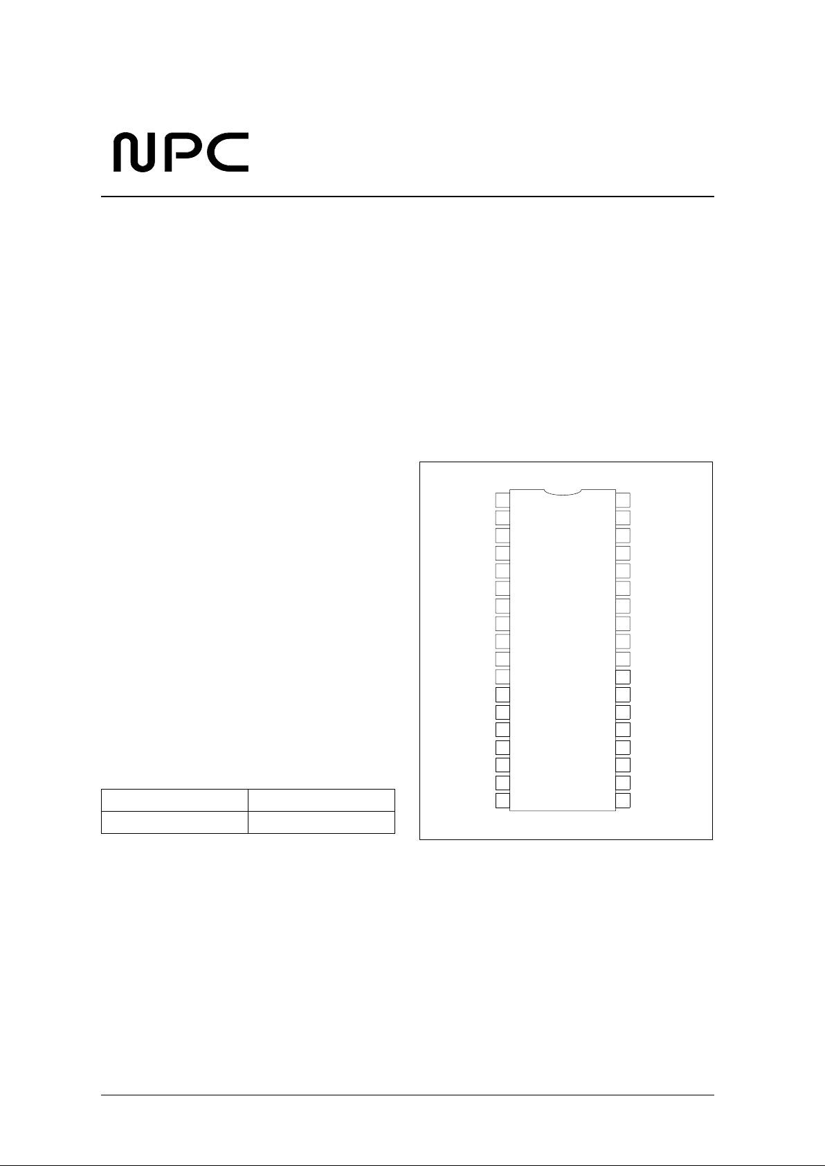
ORDERING INFORMATION
PINOUT
36-pin SSOP (Top View)
De vice Pack ag e
SM9403BM 36-pin SSOP
1NC
2NC
3FER
4FHOLD
5FSUB
6ISET
7DPDD
8DPDC
9DPDB
10DPDA
11AGND
12MMTI
13CAPAN
14CAPAP
15CAPLFC
16TSUB
17THOLD
18TRE 19 VREF4
20 VREF2
21 TROFF
22 TRP
23 CAPAREA
24 CAPOUT
25 AVCC
26 CAPIN
27 CAPSEL
28 CAPSEEK
29 DVCC
30 SENB
31 SDATA
32 SCLK
33 DGND
34 DEFECT
35 DPDI
36 DPDG
SM9403BM
NPC
Page 2
SM9403BM
NIPPON PRECISION CIRCUITS—2
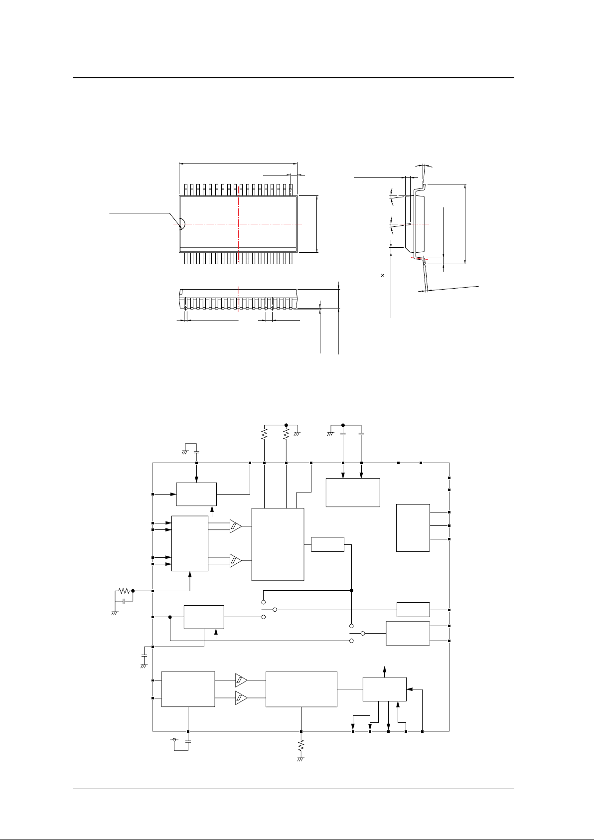
PACKAGE DIMENSIONS
(Unit: mm)
BLOCK DIAGRAM
2.44 to 2.64
0.85
15.20 to 15.40
7.40 to 7.60
0.29 to 0.39
0.80
0.10 to 0.30
0.51 to 1.01
10.11 to 10.51
0.63 ± 0.10
7°
0 to 8°
0.23 to 0.32
7°
0.51 ± 0.20 45°
R0.63 to 0.89
Phase
comparator
LPF
Voltage
reference
S / H
LPF
Serial
interface
S / H
control
DPDI
DPDG
ISET
VREF2
VREF4
FER
FHOLD
FSUB
TSUB
THOLD
CAPAP
CAPAN
CAPLFC
CAPIN
CAPOUT
CAPAREA
CAPSEL
CAPSEEK
TRP
TROFF
TRE
SENB
SDATA
SCLK
DGND
DVCC
AGND
AVCC
VREF2
DPDA
DPDB
DPDC
DPDD
Mono-multiviblator
Equalizer
Delay
LPF
Analog signal
processor
S / H
MMTI
SWB
Track Pulse
Generator
SWA
DEFECT
*
*
*
Page 3

SM9403BM
NIPPON PRECISION CIRCUITS—3
PIN DESCRIPTION
Number Name I/O
1
1. I = input, Ipd = Input with built-in pull-down resistor, I/O = input/output (N-channel open-drain when output), O = output
Function
1 N C O No connection
2 N C O No connection
3 F E R O Focus error signal output
4 FHOLD – Focus error hold capacitor connection
5 FSUB I Focus error signal input
6 ISET I DPD signal equalizer, reference current set resistor connection
7 DPDD I DPD signal input D
8 DPDC I DPD signal input C
9 DPDB I DPD signal input B
10 D P DA I DPD signal input A
11 AG ND – Analog circuit ground
12 MMTI I Mono-multivibrator time-constant set resistor connection
13 C APAN I ID data signal differential inverting input
14 C APAP I ID data signal differential non-inver ting input
15 CAPLFC – Slice-level detect capacitor connection
16 TSUB I Tracking error signal input
17 THOLD – Tracking error hold capacitor connection
18 T R E O Tracking error signal output
19 VREF4 O 4V reference voltage output
20 VREF2 O 2V reference voltage output
21 TROF F O Off-trac k detect signal output. L OW when off-tra ck.
22 TRP O Track count pulse output. HIGH-level pulse for land to outer tracking.
23 CAPAREA O ID interval detect signal output. ID interval detected when HIGH.
24 CAPOUT O Outer offset ID detect signal output. Outer offset ID interval detected when HIGH.
25 AVCC – Analog circuit pow er supply
26 CAPIN O Inner offset ID detect signal output. Inner offset ID interval detected when HIGH.
27 CAPSEL Ipd ID interval signal input. ID interva l selected when HIGH.
28 CAPSEEK Ipd Seek operation signal input. Seek operation selected when HIGH.
29 DVC C – Logic circuit pow er supply
30 SENB I Serial interface enable input. Enabled when HIGH.
31 SDA TA I/O Serial interface data input/ackno wledge output
32 SCLK I Serial interface clock input
33 DGND – Logic circuit ground
34 DEFECT Ipd Defect position signal input. Defect position indicated when HIGH.
35 DPDI I DPD signal hold delay set resistor connection
36 DPDG I DPD signal phase difference to voltage converter coefficient set resistor connection
Page 4
SM9403BM
NIPPON PRECISION CIRCUITS—4
SPECIFICATIONS
Absolute Maximum Ratings
GND = 0 V
Recommended Operating Conditions
GND = 0 V
Recommended External Components
Parameter Symbol Condition Rating Unit
Supply voltage range V
CC
−
0.5 to 7.0 V
Input voltage range V
IN
−
0.5 to VCC + 0.5 V
Operating temperature range T
opr
0 to 70
°
C
Storage temperature range T
stg
−
40 to 125
°
C
Po w er dissipation P
D
250 m W
Soldering temperature T
sld
260
°
C
Soldering time t
sld
10 s
Parameter Symbol Condition Rating Unit
Specifications supply voltage range V
CC
4.75 to 5.25 V
Operating supply voltage range V
CC
4.5 to 5.5 V
Operating temperature range T
opr
0 to 70
°
C
Pin No. Pin name Component Tolerance
4 FHOLD 1000pF capacitor K (±10%)
6 ISET
47kΩ resistor ± 1%
0.01µF capacitor Z (+80% to −20%)
12 MMTI 120kΩ resistor ± 1%
15 CAPLFC 0.01µF capacitor Z (+80% to −20%)
17 THOLD 1000pF capacitor K (±10%)
19 VREF4 0.1µF capacitor Z (+80% to −20%)
20 VREF2 0.1µF capacitor Z (+80% to −20%)
35 DPDI 47kΩ resistor ± 1%
36 DPDG 33k
Ω
resistor ± 1%
Page 5

SM9403BM
NIPPON PRECISION CIRCUITS—5
DC Electrical Characteristics
VCC = 5V ± 5%, GND = 0V, Ta = 0 to 70°C
Parameter Symbol Condition
Rating
Unit
min typ ma x
Current consumption
1
1. 33kΩ resistor connected between DPDG and AGN D 47kΩ resistor connected between DPDI and AGN D
120kΩ resistor connected between MMTI and AGN D 47kΩ resistor connected between ISET and AGN D
1000pF capacitor connected between FHOLD and AGN D 1000pF capacitor connected between THOLD and AG ND
0.1µF capacitor connected between VREF4 and AG ND 0.1µF capacitor connected between VREF2 and AG ND
0.01µF capacitor connected between CAPLFC and AGN D 0.01µF capacitor connected between ISET and AGN D
CA PAP, CAPAN, DPDA, DPDB, DPDC, DPDD, FSUB, TSUB connected to VREF2 or other 2V supply.
SENB, SDATA, SCLK connected to GND; All other pins (excluding supply and ground pins) open circuit.
Sleep mode 1: DPD system only in sleep condition.
Sleep mode 2: All block s except reference supply voltage generator in sleep condition.
Sleep mode 3: All blocks i n sleep condition.
I
CC1
Operating mode – 28 34
mA
I
CC2
Sleep mode 1 – 17 21
I
CC3
Sleep mode 2 – 2.0 2.6
I
CC4
Sleep mode 3 – – 1.0
∆
I
CCICC1
− I
CC2
9––
CAPSEEK, CAPSEL, DEFECT, SENB, SDATA,
SCLK HIGH-level input voltage
V
IH
0.8V
CC
––V
CAPSEEK, CAPSEL, DEFECT, SENB, SDATA,
SCLK LOW-level input voltage
V
IL
– – 0.2V
CC
V
CAPSEEK, CAPSEL, DEFECT HIGH-level input
current
I
IH1
VIN = V
CC
50 100 200 µ A
SENB, SDATA, SCLK HIGH-level input current I
IH2
VIN = V
CC
––3µA
CAPSEEK, CAPSEL, DEFECT, SENB, SDATA,
SCLK LOW-level input current
I
IL
VIN = GND
−
3– –µA
CA PAREA, CAPIN, CAPOUT, TR P, TROFF
HIGH-level output voltage
V
OHIOH
= −0.2mA VCC − 0.2 – – V
CA PAREA, CAPIN, CAPOUT, TR P, TROFF
L O W-level output voltage
V
OL1IOL
= 0.8mA – – 0.4 V
S D ATA L OW -level output voltage V
OL2IOL
= 7mA – – 1.0 V
Page 6
SM9403BM
NIPPON PRECISION CIRCUITS—6
Focus Sample-and-Hold, Low-pass Filter Characteristics (FSUB → FER)
VCC = 5V ± 5%, GND = 0V, Ta = 0 to 70°C, FSUB and FER signals in phase
Tracking Sample-and-Hold, Low-pass Filter Characteristics (TSUB → TRE)
VCC = 5V ± 5%, GND = 0V, Ta = 0 to 70°C, TSUB and TRE signals in phase
Parameter Condition
Rating
Unit
min typ ma x
FSUB input signal range VREF2 reference
−
1.25 0 +1.25 V
FER output voltage range VREF2 reference
−
1.25 0 +1.25 V
FER output offset voltage VREF2 reference, VIN = V
REF2
– – ±8.0 m V
FER output offset voltage temperature drift VREF2 reference – – ±45 µV/°C
FER output signal slew rate LPF off 1 – – V/µs
FER output load regulation I
OUT
= ±3mA, VIN = V
REF2
– – ±10 mV
FSUB input impedance 100 – – k
Ω
FER output signal gain
−
0.17 0 +0.17 dB
FER output signal bandwidth
1
1. CL = 20pF, RL = 500
Ω
VIN = 1.5Vp-p,
−
3dB from DC
LPF off (FFE = HIGH) 500 – –
kHz
LPF on (FFE = LOW) 11 5 160 23 0
FER output gain peaking
1
DC to −3dB frequency
−
3 – +0.5 dB
Hold time FER output droop characteristic VIN = 200mVp-p, C
FHOLD
= 1000pF – – 0.025 %/µs
S/H acquisition time
∆
VIN = 200mV, target value ± 10% – – 1 µs
FER output hold error With respect to the previous value – – ±4 mV
Pow er-down state FER output impedance 1 – – M
Ω
Parameter Condition
Rating
Unit
min typ ma x
TSUB input signal range VREF2 reference
−
1.25 0 +1.25 V
TRE output voltage range VREF2 reference
−
1.25 0 +1.25 V
TRE output offset voltage VREF2 reference, VIN = V
REF2
– – ±8.0 m V
TRE output offset voltage temperature drift VREF2 reference – – ±45 µV/
°
C
TRE output load regulation I
OUT
= ±3mA, VIN = V
REF2
– – ±10 mV
TSUB input impedance 100 – – k
Ω
TRE output signal gain
−
0.17 0 +0.17 dB
TRE output signal bandwidth
1
1. CL = 20pF, RL = 500
Ω
VIN = 1.5Vp-p,
−
3dB from DC
TFE = HIGH 24 35 50
kHz
TFE = LOW 115 160 230
TRE output gain peaking
1
DC to −3dB frequency
−
3 – +0.5 dB
Hold time TRE output droop characteristic VIN = 200mVp-p, C
THOLD
= 1000pF – – 0.025 %/µs
S/H acquisition time
∆
VIN = 200mV, target value ±10% – – 1 µs
TRE output hold error With respect to the previous value – – ±4 mV
Power-down state TRE output impedance 1 – – M
Ω
Page 7

SM9403BM
NIPPON PRECISION CIRCUITS—7
DPD Error Signal Detector Characteristics (DPDA/DPDB/DPDC/DPDD → TRP)
VCC = 5V ± 5%, GND = 0V, Ta = 0 to 70°C
Parameter
1
1. The tracking error signal TRE is positive with respect to VREF2 if the (DPDA + DPDC) signal phase difference is leading.
The detected phase difference is the difference between the point when one internal comparator output changes (from CMA and CMB both HIGH or
both LOW) until the second output changes before the first changes again. The phase difference is conver ted to a voltage and sampled for output.
Other signals are held constant in the output stage when a phase difference is detected.
Condition
Rating
Unit
min typ ma x
DP DA/DPDB/DPDC/DPDD input voltage
range
VREF2 reference
−
0.55 – +1 V
DP DA/DPDB/DPDC/DPDD input
impedance
1––MΩ
Signal gain relative accuracy
Gain relative to DP DA, DPDB, DPDC,
DPDD inputs
– – ±0.17 d B
Equalizer gain
1MHz setting
DG2 =LOW 1.2 1.6 2.3
dB
DG2 = HIGH 1.8 2.2 2.9
5MHz setting
DG2 =LOW 5.5 6.1 6.6
DG2 = HIGH 6.1 6.7 7.2
Equalizer frequency response
Peak gain frequency (EQE = HIGH) 3.75 5.0 6.25
MHz
−
3dB frequency (EQE = LOW) 11 22 33
Equalizer frequency response relative
accuracy
f
peak
, (A + C) vs. (B + D) – – ±1.5 %
AC coupling time circuit
−
3dB frequency
Time constant 1 DG2 = LOW 56 84 109
kHz
Time constant 2 DG2 = HIGH 17 24 32
AC coupling time constant relative
accuracy
−
3dB frequency, (A + C) vs. (B + D) – – ±2 %
Delay control range See table 4. See table 4. ns
Phase difference detector minimum time DG1 = DG2 = LOW 2 – – ns
Phase difference detector maximum time DG1 = DG2 = HIGH – – 1 µs
Phase difference detector minimum
repeat time
Input pulse interval 12 0 – – n s
Phase difference to voltage conversion
coefficient
DG1 = DG2 = LOW – See table 5. typ ± 20% mV/ns
Phase difference to voltage conversion
coefficient change accuracy
– See table 8. ±1 d B
Phase difference output offset voltage VREF2 reference – – ±0.1 V
Phase difference output offset voltage
temperature drift
VREF2 reference – – ±570 µV/
°
C
DEFECT signal response time – – 1 µs
DPD enable response time DPE flag – – 2 µs
Abnormal waveform TRP droop
characteristic
V
OUT
= V
REF2
± 200mV, VREF2 reference – – 0.1 %/µs
TRP output voltage range VREF2 reference
−
1.25 0 +1.25 V
TRP output signal frequency response−3dB frequency 500 – – kHz
Page 8

SM9403BM
NIPPON PRECISION CIRCUITS—8
Header Position Detector Characteristics (CAPAP/N → CAPAREA, CAPIN, CAPOUT)
VCC = 5V ± 5%, GND = 0V, Ta = 0 to 70°C
Sample-and-Hold Control Signal Generator Characteristics
VCC = 5V ± 5%, GND = 0V, Ta = 0 to 70°C
Tracking Error Signal Switching Characteristics (SWA, SWB)
VCC = 5V ± 5%, GND = 0V, Ta = 0 to 70°C
Parameter Condition
Rating
Unit
min typ ma x
C A PAP/N input voltage range 1 – 3 V
Analog signal processor frequency
response
V
IN
= V
REF2
± 0.5V, −3dB from DC 13 – – M Hz
Analog signal quantization slice level – See table 9. typ ± 15% V
Mono-multivibrator time constant typ
−
5% See table 10. typ + 45% µs
Mono-multivibrator time constant switching
accuracy
––±5%
Mono-multivibrator time-constant block
interval accurac y
– – ±2.5 %
CAPIN, CAPOUT, CAPAREA output r ise
time and fall time
C
L
= 20pF – – 15 n s
Parameter Condition
Rating
Unit
min typ ma x
FER, TRE output response time
1
1. FSHCNT and TSHCNT are the focus and tracking sample-and-hold internal control signals, respectively.
Mono-multivibrator/CAPSEL/CAPSEEK
→
FSHCNT/TSHCNT
– – 100 ns
Serial interface (HRE, FHE, THE, HAE)
→
FSHCNT/TSHCNT
––2µs
Parameter Condition
Rating
Unit
min typ ma x
Switching response time Serial interface timing – – 1 µs
Page 9

SM9403BM
NIPPON PRECISION CIRCUITS—9
Track Count Pulse Generator Characteristics (TSUB → TRP , TROFF)
VCC = 5V ± 5%, GND = 0V, Ta = 0 to 70°C
Reference Voltage Generator Characteristics (VREF2, VREF4)
VCC = 5V ± 5%, GND = 0V, Ta = 0 to 70°C
Parameter Condition
Rating
Unit
min typ ma x
TSUB input signal range VREF2 reference
−
1.25 – +1.25 V
TSUB signal limiter voltage level VREF2 reference ±1.0 – – V
TSUB signal amplifier gain f = 5kHz 5.83 6.0 6.17 d B
Quantization level offset set value typ − 15 % See table 15 typ + 15% m V
TRP output comparator hysteresis
1
1. TRP has the same polarity as TRE (i.e. TRP is HIGH when TRE > VREF2).
T ROFF is HIGH when the input signal is inside the window , and LOW when outside the window.
typ − 10 % See table 16 typ + 10% m V
TRP output comparator hysteresis
response time
Minimum hysteresis, target value ± 10% – – 600 n s
TRP output comparator hysteresis
switching response time
Minimum
↔
maximum hysteresis value – – 2 µs
TR OFF output comparator window typ
−
10 % See table 17 typ + 10% m V
TR OFF output comparator window
switching response time
Minimum
↔
maximum window value – – 5 µs
Parameter Condition
Rating
Unit
min typ ma x
VREF4 output voltage
V
CC
= 5V, Ta = 25°C, I
OUT
= 0
3.84 4.0 4.16 V
VREF2 output voltage 1.92 2.0 2.08 V
VREF4 output voltage temperature drift
VCC = 5V, Ta = 0 to 70°C, I
OUT
= 0
– – ±400 µV/°C
VREF2 output voltage temperature drift – – ±200 µV/°C
VREF4 output voltage supply voltage
dependency
V
CC
= 5V ± 5%, Ta = 25°C, I
OUT
= 0
––±6mV
VREF2 output voltage supply voltage
dependency
––±3mV
VREF4 output voltage load regulation
V
CC
= 5V,
Ta = 25°C
I
OUT
= 0 to 8mA – –
−
20 m V
VREF2 output voltage load regulation I
OUT
= 0 to ±5mA – – ± 10 m V
Relative output voltage accuracy
1
1. De fined as (VREF2 − (VREF4 ÷ 2)).
VCC = 5V, I
OUT
= 0 – – ± 20 m V
Relative output voltage temperature drift VCC = 5V, Ta = 0 to 70°C, I
OUT
= 0 – – ± 10 µ V/°C
Relative output-voltage supply-voltage
dependency
V
CC
= 5V ± 5%, Ta = 25°C, I
OUT
= 0 – – ±1 mV
VREF4 power-down output impedance 13 – – kΩ
VREF2 power-down output impedance 1 – – M Ω
Page 10

SM9403BM
NIPPON PRECISION CIRCUITS—10
Serial Interface Characteristics (SCLK, SDATA, SENB)
VCC = 5V ± 5%, GND = 0V, Ta = 0 to 70°C
Parameter Symbol Condition
Rating
Unit
min typ ma x
SCLK pulse cycle t
cySCK
100 – – ns
SCLK HIGH-level pulsewidth t
whSCK
40 – – ns
SCLK LOW-level pulsewidth t
wlSCK
40 – – ns
SENB setup time t
sSEN
20 – – ns
SENB hold time t
hSEN
40 – – ns
S DATA setup time t
sSDA
15 – – ns
S DATA hold time t
hSDA
15 – – ns
ACK setup time
1
1. A CK is the ackno wledge output (n-channel open-drain). LOW -level output when the data received is valid.
S DATA load capacitance is 15pF.
t
sACK
0–20ns
ACK hold time
1
t
hACK
––50ns
SENB interval t
inSEN
100 – – ns
SENB
SCLOCK
SDATA
Controller
SDATA
Port
tsSEN twhSCK twlCLK
tcySCK
tsSDA
thSDA
tsACK
thACK
tinSEN
thSEN
bit 0 bit 1
bit 15
LSB MSB
ACK
High Impedance
Page 11

SM9403BM
NIPPON PRECISION CIRCUITS—11
FUNCTIONAL DESCRIPTION
Serial Interface
The SM9403BM uses a serial interface comprising 5
ports to control and set all functions. The address and
bit configuration of each port is shown in table 1
Serial data is input on SDATA with the LSB first, in
sync with the falling edge of the SCLK clock. After
the 16th SCLK falling edge and 16 bits of valid data
has been input, the SDATA n-channel open-drain
output goes LOW as an acknowledge signal.
If the number of SCLK cycles which occur when
SENB (serial interface enable) is HIGH is less than
16, the received data is ignored and the internal port
is not updated. If the number of SCLK cycles is
greater than 16, the data is still considered value up
to the 16th SCLK falling edge, the data is latched
into the internal port, and the acknowledge signal is
output. The acknowledge signal is held until SENB
goes LOW again.
Focus Sample-and-Hold/Low-pass Filter (FSUB → FER)
This stage, the signal which is generated from the
header position detector signal samples and holds the
focus error signal. The output then passes through a
low-pass filter. This low-pass filter can be turned ON
or OFF using the serial interface control bit FFE.
Tracking Sample-and-Hold/Low-pass Filter (TSUB → TRE)
This stage, the signal which is generated from the
header position detector signal samples and holds the
tracking error signal. The output then passes through
a low-pass filter . This lo w-pass filter cutof f frequenc y
can be switched using the serial interface control bit
TFE.
Table 1. Port address and bit configuration
1
Bit number
1514131211109876543210
Data Ad dress
MSB LSB
DPE HAE FFE TFE SWB SWA SL2 SL1
×
LOW LOW LOW HIGH LOW
××
OF3 OF2 OF1 WD2 WD 1 HS3 HS2 HS1
×
LOW LOW LOW HIGH HIGH
××
THE FHE HRE MM 2 M M1 LS3 LS2 LS1
×
LOW LOW HIGH LOW LOW
××
EQE CG3 CG 2 CG1 DL4 DL3 DL2 DL1
×
LOW LOW HIGH LOW HIGH
××
TS3 TS2 TS1 – – – D G2 DG 1
×
LOW LOW HIGH HIGH LOW
××
1.× = don’t care, – = unassigned
Table 2. Focus low-pass filter ON/OFF control
FFE Lo w-pass filter
1
LOW ON
HIGH OFF
1. D efault is ON
Table 3. Tracking low-pass filter cutoff frequency
TFE Lo w-pass filter
1
LOW fC = 160kHz
HIGH fC = 35kHz
1. D efault is 160kHz
Page 12

SM9403BM
NIPPON PRECISION CIRCUITS—12
DPD Error Signal Detector (DPDA/DPDB/DPDC/DPDD → TRP)
This stage compares the DPD signals, passes the
comparator output through a low-pass filter to obtain
the DPD tracking error signal.
The DPD signals are first added, (DPDA + DPDC)
and (DPDB + DPDD), then passed to an equalizer. A
relative time delay is added for offset correction. The
signals are then converted to a pulse waveform by
comparators with hysteresis characteristics.
The phase comparator then compares the phase of
the pulse waveforms to obtain a time signal equivalent to the tracking error. The time signal is then converted to a voltage.
The converted voltage is passed to the output stage,
undergoes sampling timing compensation before
being integrated to generate the tracking error signal
output.
The phase comparator incorporates a detector function which prevents abnormal waveform signals getting to the output by holding the output constant.
In addition, serial interface control bit DPE and input
DEFECT can be used to force the tracking error signal to the reference voltage VREF2. These controls
can be used when powering up a system or to prevent
output saturation from occurring during periods
when the input signal is unstable.
The relative time delay setting and time-to-voltage
conversion coefficient can be controlled using serial
interface control bits. Also, the equalizer used to
compensate for the previous stage can be turned ON
or OFF using serial interface control.
Page 13

SM9403BM
NIPPON PRECISION CIRCUITS—13
Table 4. DPD delay time settings
DG2 DG1 DL4 DL3 DL2 DL1
DPD delay (ns)
1
min typ max
LOW LOW
LOW LOW LOW LOW 0 0 0
LOW LOW LOW HIGH−2.2−3.0−3.3
LOW LOW HIGH LOW−4.2−5.6−6.4
LOW LOW HIGH HIGH−6.0−8.0−9.5
LOW HIGH LOW LOW−7.5−11−13
LOW HIGH LOW HIGH−10−14−16
LOW HIGH HIGH LOW−12−17−20
LOW HIGH HIGH HIGH−14−20−24
HIGH LOW LOW LOW +17 +24 +29
HIGH LOW LOW HIGH +14 +20 +23
HIGH LOW HIGH LOW +12 +17 +19
HIGH LOW HIGH HIGH +10 +13 +15
HIGH HIGH LOW LOW +7.5 +1 1 +13
HIGH HIGH LOW HIGH +5.6 +7.7 +9.0
HIGH HIGH HIGH LOW +3.7 +5.5 +6.2
HIGH HIGH HIGH HIGH +2.0 +3.0 +3.4
LOW HIGH
LOW LOW LOW LOW 0 0 0
LOW LOW LOW HIGH−3.8−4.5−6.0
LOW LOW HIGH LOW−7.0−8.5−11
LOW LOW HIGH HIGH−11−13−17
LOW HIGH LOW LOW−16−18−24
LOW HIGH LOW HIGH−20−23−32
LOW HIGH HIGH LOW−26−30−42
LOW HIGH HIGH HIGH−34−38−55
HIGH LOW LOW LOW +44 +49 +74
HIGH LOW LOW HIGH +33 +37 +52
HIGH LOW HIGH LOW +25 +29 +38
HIGH LOW HIGH HIGH +20 +22 +29
HIGH HIGH LOW LOW +15 +17 +22
HIGH HIGH LOW HIGH +10 +12 +17
HIGH HIGH HIGH LOW +7.0 +7.9 +11
HIGH HIGH HIGH HIGH +3.6 +4.3 +5.6
HIGH LOW
LOW LOW LOW LOW 0 0 0
LOW LOW LOW HIGH−7.0−8.5−13
LOW LOW HIGH LOW−15−17−24
LOW LOW HIGH HIGH−22−27−36
LOW HIGH LOW LOW−32−37−50
LOW HIGH LOW HIGH−43−48−65
LOW HIGH HIGH LOW−55−62−83
LOW HIGH HIGH HIGH−70−78−108
HIGH LOW LOW LOW +90 +100 +136
HIGH LOW LOW HIGH +70 +78 +102
HIGH LOW HIGH LOW +55 +61 +76
HIGH LOW HIGH HIGH +42 +47 +60
HIGH HIGH LOW LOW +31 +36 +45
HIGH HIGH LOW HIGH +22 +26 +34
HIGH HIGH HIGH LOW +14 +17 +23
HIGH HIGH HIGH HIGH +7.2 +8.2 +12
HIGH HIGH
LOW LOW LOW LOW 0 0 0
LOW LOW LOW HIGH−9.5−11−17
LOW LOW HIGH LOW−19−22−32
LOW LOW HIGH HIGH−30−35−49
LOW HIGH LOW LOW−42−48−74
LOW HIGH LOW HIGH−60−67−105
LOW HIGH HIGH LOW−80−90−150
LOW HIGH HIGH HIGH−110−122−205
HIGH LOW LOW LOW +124 +167 +210
HIGH LOW LOW HIGH +108 +120 +194
HIGH LOW HIGH LOW +80 +88 +130
HIGH LOW HIGH HIGH +58 +65 +90
HIGH HIGH LOW LOW +42 +47 +64
HIGH HIGH LOW HIGH +29 +33 +45
HIGH HIGH HIGH LOW +18 +21 +31
HIGH HIGH HIGH HIGH +9.0 +10 + 16
1. De fault is 0 ns (DL4 = DL3 = DL2 = DL1 = LOW)
The DPD delay is positive when (A+C) leads (B+D).
Table 4. DPD delay time settings (Continued)
DG2 DG1 DL4 DL3 DL2 DL1
DPD delay (ns)
1
min typ max
Page 14

SM9403BM
NIPPON PRECISION CIRCUITS—14
Table 5. Phase difference to voltage converter
coefficient
CG3 CG2 CG1
Coefficient
(mV/ns)
1
LO W L OW L OW 5.38
LOW L OW HIGH 7.58
LOW HIGH LOW 10.7
LOW HIGH HIGH 15.2
HIGH LOW LOW 21.4
HIGH LOW HIGH 30.3
HIGH HIGH LOW 42.7
HIGH HIGH HIGH 60.6
1. D efault is 15.2 mV/ns
Table 6. Equalizer control
EQ E Equalizer
1
LOW OFF
HIGH O N
1. D efault is OFF
Table 7. DPD output control
DPE DEFECT DPD output
1
LOW
×
Forced to VREF2
×
HIGH Forced to VREF2
HIGH LOW Active
1. D e f ault is VREF2 (DPE = LOW)
Table 8. DPD delay time coefficient, phase diff erence to v oltage converter coefficient, AC coupling time constant
DG2 DG1
Phase to voltage coefficient
(relative to values in table 5)
1
DPD-AC coupling time
constant circuit −3dB
frequency
Selected media
LOW LOW
×
1
100 kHz
8-times CD, DVD-RAM
LOW HIGH
×
1/2 4-times CD
HIGH L OW
×
1/4
25 kHz
2-times CD
HIGH HIGH
×
1/8 1-times CD
1. Default is DG2 = DG1 = LOW
Page 15

SM9403BM
NIPPON PRECISION CIRCUITS—15
Header Position Detector (CAPAP/N → CAPAREA, CAPIN, CAPOUT)
This stage converts a high-speed push-pull signal
(CAPAP/CAPAN) to single-ended signals, passes
the outputs through low-pass filters to form quantized logic levels which are used as reference signals.
These reference signals are level shifted to form plus
and minus signals for use by comparators. The
amount of level shift can be controlled by serial
interface control bits.
After quantization logic conversion, retriggerable
mono-multivibrators conv ert the pulse strings to con-
tinuous signals. This creates inner shifted header
CAPIN and an outer shifted header CAPOUT output
signals.
In addition, the single-ended signal is also passed
through a high-pass filter, which similarly converts
to quantized logic signals. Retriggerable mono-multivibrators then convert the pulse strings to continuous signals to create a header area CAPAREA signal.
The mono-multivibrator time constants are controlled by serial interface control bits.
Table 9. Slice level shift voltages
LS3 LS2 LS1
Le vel shift
(mV)
1
1. D efault is ±25 mV
LOW LOW LOW ±25
LOW LOW HIGH ±50
LOW HIGH L OW ±75
LOW HIGH HIGH ±100
HIGH LOW LOW ±125
HIGH LOW HIGH ±150
HIGH HIGH LOW ±200
HIGH HIGH HIGH ±250
Table 10. Mono-multivibrator time constants
MM2 MM1
CAPOUT/CAPIN
output (µs)
1
1. Def ault is 4 µs and (8 + α), where α ≈ 6 × ln(2VLS/VH), VH = input signal amplitude, V
LS
= slice level absolute value shown in table 9.
CA PAREA (µs)
1
L O W L O W 4 8 +
α
LOW HIGH 8 16 +
α
HIGH LOW 12 24 +
α
HIGH HIGH 16 32 +
α
Table 11. CAPOUT/CAPIN/CAPAREA logic
CAPARE
A
HAE
1
1. Default is LOW
CAPOUT CAPIN
LOW LOW
Header signal
output
Header signal
output
LOW HIGH LOW LOW
HIGH L OW
Header signal
output
Header signal
output
HIGH HIGH
Header signal
output
Header signal
output
Page 16

SM9403BM
NIPPON PRECISION CIRCUITS—16
Sample-and-Hold Control Signal Generator
This stage takes the OR-logic of the CAPIN and
CAPOUT signals, generated by the header position
detector, the CAPSEL and CAPSEEK input signals,
and the serial interface control bit HRE and uses
them to create a sample-and-hold circuit control signal SHCNT.
The SHCNT is then used in conjunction with serial
interface select bits FHE and THE to form the focus
sample-and-hold (FSHCNT) and tracking sampleand-hold (TSHCNT) signals.
×
= don’t care.
×
= don’t care.
Tracking Error Signal Switching (SWA, SWB)
This stage performs tracking error signal switching
during DVDRAM write/read and DVDROM and CD
playback. Switching is controlled by serial interface
control bits.
Table 12. Sample-and-hold logic
CAPIN CAPOUT CAPSEL CAPSEEK HRE
1
SHCNT
HIGH
××
LOW HIGH HIGH
×
HIGH
×
LOW HIGH HIGH
LOW LOW
×
LOW
×
LOW
HIGH
××
LOW LOW LOW
×
HIGH
×
LOW LOW LOW
××
HIGH HIGH
×
HIGH
××
LOW HIGH
×
LOW
1. Default is LOW
Table 13. Sample-and-hold signal control logic
FHE
1
1. Default is LOW
THE
1
FSHCNT
2
2. FSHCNT is the focus sample-and-hold control signal, and TSHCNT is
the trac king sample-and-hold control signal.
TSHCNT
2
LOW
×
LOW
×
×
LOW
×
LOW
HIGH
×
SHCNT
×
×
HIGH
×
SHCNT
Table 14. Tracking error signal select
SWA SWB
Tracking error
signal select
1
1. Def ault is S/H
LOW LOW S/H
HIGH HIGH DPD
Page 17

SM9403BM
NIPPON PRECISION CIRCUITS—17
Track Count Pulse Generator (TSUB → TRP , TROFF)
This stage filters the tracking error signal through a
6th-order Butterworth low-pass filter which effectively filters off header signal leakage effects. An of fset voltage is added and the signal passes through a
comparator with hysteresis to generate a track count
pulse signal output on TRP. Simultaneously, the window comparator corresponding to the tracking error
signal is output as the off-track signal on TROFF
(LOW for off-track).
The offset voltage, hysteresis level and window
width are controlled by serial interface bits.
Sleep Mode
The SM9403BM features 3 sleep modes which can
be used when the device is not operating to signifi-
cantly reduce current consumption. The sleep modes
are controlled by serial interface bits.
Preset Function
When power is applied or in sleep modes 2 and 3, all
serial interface flags are reset to their default values
with the exception of the sleep mode flags SL2 and
SL1 (see the section “Serial Interface”). However,
when writing data to SL2 and SL1 to cancel sleep
mode, other flags in the same data word have precedence when writing to the port.
Table 15. Offset voltage setting
OF 3 OF 2 OF 1 Offset voltage (mV)
1
1. D efault is 0 mV
LOW LOW LOW 0
LOW LOW HIGH
−
200
LOW HIGH LOW
−
400
LOW HIGH HIGH
−
600
HIGH LOW LOW +800
HIGH LOW HIGH +600
HIGH HIGH LOW +400
HIGH HIGH HIGH +200
Table 16. TRP comparator hysteresis
HS 3 H S 2 H S1 Hysteresis (mV)
1
LOW L OW L OW ±100
LOW LOW HIGH ±200
LOW HIGH LOW ±300
LOW HIGH HIGH ±400
HIGH LOW LOW ±500
HIGH LOW HIGH ≥ 500
HIGH HIGH LOW ≥ 500
HIGH HIGH HIGH ≥ 500
1. D efault is ±100 mV
Table 17. TROFF comparator window
WD2 WD1
Comparator
window (mV)
1
LOW LOW ±125
LOW HIGH ±250
HIGH LOW ±375
HIGH HIGH ±475
1. D efault is ±125 mV
Table 18. Sleep mode settings
SL2 SL 1 Mode description
1
1. De fault is OFF (SL2 = SL1 = LOW)
LO W LO W Sleep mode OFF (normal operation)
LOW HIGH DPD in sleep condition
HIGH LOW
All except reference voltage supply in
sleep condition
HIGH HIGH All blocks i n sleep condition
Page 18

SM9403BM
NIPPON PRECISION CIRCUITS—18
NIPPON PRECISION CIRCUITS INC. reserves the right to make changes to the products described in this data sheet in order to
improve the design or performance and to supply the best possible products. Nippon Precision Circuits Inc. assumes no responsibility for
the use of any circuits shown in this data sheet, conveys no license under any patent or other rights, and makes no claim that the circuits
are free from patent infringement. Applications for any devices shown in this data sheet are for illustration only and Nippon Precision
Circuits Inc. makes no claim or warranty that such applications will be suitable for the use specified without further testing or modification.
The products described in this data sheet are not intended to use for the apparatus which influence human lives due to the failure or
malfunction of the products. Customers are requested to comply with applicable laws and regulations in effect now and hereinafter,
including compliance with export controls on the distribution or dissemination of the products. Customers shall not export, directly or
indirectly, any products without first obtaining required licenses and approvals from appropriate government agencies.
NIPPON PRECISION CIRCUITS INC.
4-3, Fukuzumi 2-chome
Koto-ku, Tokyo 135-8430, Japan
Telephone: 03-3642-6661
Facsimile: 03-3642-6698
NC9813AE 1999.09
NIPPON PRECISION CIRCUITS INC.
 Loading...