

Page 1
SM1350 series
NIPPON PRECISION CIRCUITS—1
NIPPON PRECISION CIRCUITS INC.
High Tone Quality Melody LSI
OVERVIEW
The SM1350 series are single-chip high tone quality
melody ICs, fabricated using NPC’s Molybdenumgate CMOS process. Melodies are selected in serial
or binary (parallel) mode, up to a maximum of 16
melody blocks. There are 4 sound generators
incorporated to produce 4 kinds of output tone
controlled by 16-tone data, making these ICs ideal
for mechanical clocks and similar applications where
high tone quality output is demanded.
FEATURES
■
Basic Functions
• 4.0 MHz oscillator frequency
• Power-save function
- Oscillator stopped when no output
- S0 to S3, MODE, LH pull-up resistors open
• BTL or A-class outputs
• Chattering prevention circuit (STN, STOP, S0
to S3)
• 10-bit D/A converter
■
Sound Generator Functions
• DWS (dual wave synthesis) sound generators
• 4 simultaneous sounds for 4 tones
• G2 to F#7 note range
• 16-tone programmable
■
Melody Functions
• Up to 16 programmable melodies (singly or in
medleys)
• 1024-step length (notes, rests, jumps, end
codes)
• Level hold/one-shot melody modes
• Serial/binary (parallel) select modes
• 4.8 to 605.6 tempo range in 127 steps
• 12 rhythm values
• Ties and slurs programmable
■
Control Signal Outputs
• BUSYN signal LOW during melody output
• CT signal output for external control
■
2.4 to 5.5 V supply voltage
■
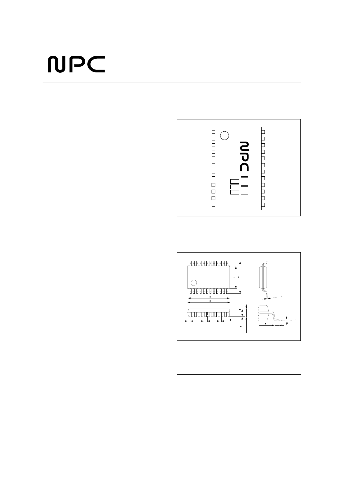
Package
• 24-pin SSOP (SM1350
×××
)
■
Molybdenum-gate CMOS
PINOUT
(TOP VIEW)
PACKAGE DIMENSIONS
24-pin SSOP (Unit: mm)
ORDERING INFOMATION
3
xx3ee3q . e q3hq .hh .w
Device Package
SM1350
×××
M 24pin SSOP
VDD
S0
S1
S2
S3
MODE
LH
XT
XTN
TO
T3N
T2N
T1N
MSBN
SM1
350
STOP MSB
STN
BUSYN
CT
SP
SPN
VOL
ICN VSS
1
12 13
24
0.7 0.8
0.36 0.10
10.20 0.30
10.05 0.20
0.10 0.10
2.10MAX
1.80 0.10
7.80 0.30
5.40 0.20
0.15
+
0.1
−
0.05
010
0.50 0.20
Page 2
SM1350 series
NIPPON PRECISION CIRCUITS—2
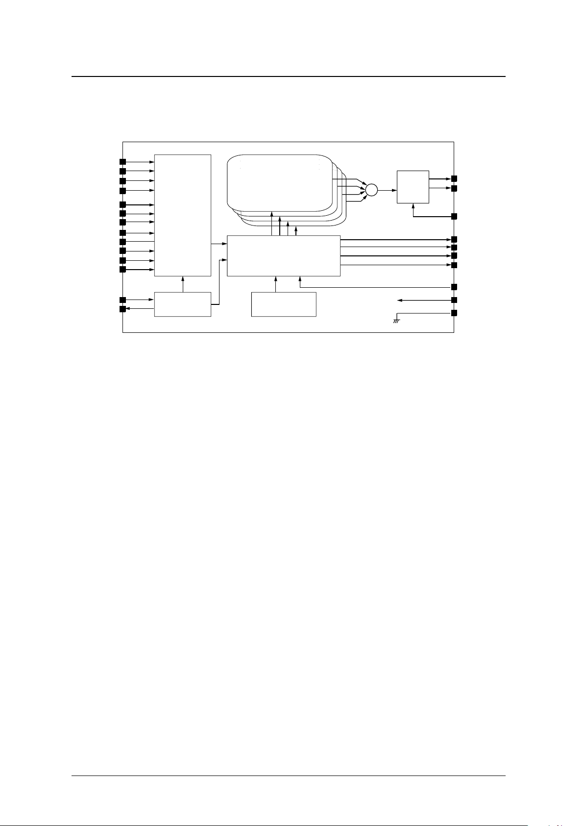
BLOCK DIAGRAM
Arithmetic block Circuit
Control Circuit
Wave ROM
Parameter ROM
Input Circuit
Score ROM
DAC
Oscillator
SP
SPN
VOL
MSB
MSBN
BUSYN
CT
S3
S2
S1
S0
MODE
LH
STOP
STN
TO
T1N
T2N
T3N
XT
XTN
+
ICN
VDD
VSS
Page 3
SM1350 series
NIPPON PRECISION CIRCUITS—3
PIN DESCRIPTION
Number Name I/O State
1
1. U = pull-up resistor connection, SU : pull-up resistor connection only when melody output starts,
P = p-channel open drain, C = complementary output.
U or O = pull-up resistance or open drain (master slice)
Description
2
2. BTL/A-class output mode is selected by mask option.
1 VDD – – Supply pin
2S0ISU
Binary select mode: Phrase select pins.
Serial select mode: S0 and S1 control melody output.
3S1ISU
4S2ISU
5S3ISU
6 MODE I SU Melody select mode control. Binary mode when LOW, and serial mode when HIGH.
7 LH I SU Melody output mode control. One-shot when LOW, and level hold when HIGH.
8 STOP I U or O
One-shot melody mode: Melody output stop control.
Level hold melody mode: Invalid input.
9 STN I U or O Melody start control
10 BUSYN O C Busy output signal. LOW when a melody is output.
11 CT O C External control pulse output
12 ICN I U Initialization clear input
13 VSS – – Ground pin
14 VOL I – Volume adjust control. Volume adjusted using an external resistor.
15 SPN O P
9-bit D/A converter output in BTL output mode.
VOL current output in A-class output mode.
16 SP O P
BTL output mode: 9-bit D/A converter output.
A-class output mode: 10-bit D/A converter output.
17 MSB
O C BTL output mode: Signed-bit output. HIGH when no melody is output.
I U A-class output mode: BUSYIN input
18 MSBN O C
BTL output mode: Signed-bit output. HIGH when no melody is output.
A-class output mode: ENDN output. HIGH when no melody is output.
19 T1N I U
Test signal inputs20 T2N I U
21 T3N I U
22 TO O C Test signal output. 62.5 kHz output when not in test mode.
23 XTN O – Oscillator output
24 XT I – Oscillator input
Page 4
SM1350 series
NIPPON PRECISION CIRCUITS—4
SPECIFICATIONS
Absolute Maximum Ratings
VSS = 0 V
Recommended Operating Conditions
VSS = 0 V
Master slice
Underlined entries are the default standard options. Throughout this datasheet, the standard options are
assumed unless otherwise specified.
U: pull-up resistance O: open input
Parameter Symbol Condition Rating Unit
Supply voltage V
DD
−
0.3 to 7.0 V
Input voltage V
IN
VSS − 0.3 to VDD + 0.3 V
Storage temperature T
stg
−
40 to 125
°
C
Power dissipation P
D
650 mW
Soldering temperature T
sld
255
°
C
Soldering time t
sld
10 s
Parameter Symbol Condition
Rating
Unit
min typ max
Supply voltage V
DD
2.4 – 5.5 V
Operating temperature T
opr
−
20 – 80
°
C
Specifications Function Selected condition
Serial-mode melody selections 1 to 16
Melody output circuit BTL / A-class
Level-hold melody select change retrigger Yes / No
Pull-up/pull-down resistance
STN U
/ O
STOP U / O
Page 5
SM1350 series
NIPPON PRECISION CIRCUITS—5
DC Characteristics
VDD = 3 V, Ta = 25 °C, VSS = 0 V, fO = 4.0 MHz
1.Supply voltage ratings shown are with oscillator running and all functions operating normally.
2.Clock frequency and duty cycle are ratings for the clock input on pin XT.
3.Output current when 20 kΩ volume control resistor is connected to VOL, and all D/A con verter bits ON, measured using the circuit of the next page.
VDD = 5 V, Ta = 25 °C, VSS = 0 V, fO = 4.0 MHz
Parameter Symbol Condition
Rating
Unit
min typ max
Minimum operating supply voltage
1
V
MIN
– – 2.4 V
Maximum operating supply voltage
1
V
MAX
5.5 – – V
Standby current consumption I
STBY
No melody output – – 1.0 µA
Operating current consumption I
DD
BUSYN, CT, TO, SP, SPN,
MSB, MSBN all open
– – 3.5 mA
XT external capacitance C
G
–30–pF
XTN external capacitance C
D
–30–pF
Clock frequency
2
f
XTI
3.8 4.0 4.2 MHz
Clock duty cycle
2
R
XTI
40 50 60 %
S0 to S3, MODE, LH, STOP, STN, ICN
HIGH-level input voltage
V
IH
VDD − 0.3 – V
DD
V
S0 to S3, MODE, LH, STOP, STN, ICN
LOW-level input voltage
V
IL
V
SS
–VSS + 0.3 V
S0 to S3, MODE, LH, STOP, STN, ICN
HIGH-level input current
I
IH
VIH = V
DD
–1020µA
S0 to S3, MODE, LH, STOP, STN, ICN
LOW-level input current
I
IL
VIL = V
SS
–1020µA
BUSYN, CT, TO HIGH-level output
current
I
OH1
V
OH1
= VDD − 0.7 2.0 – – mA
BUSYN, CT , TO LOW-lev el output current I
OL1
V
OL1
= VSS + 0.7 2.0 – – mA
MSB , MSBN HIGH-level output current I
OH2
V
OH2
= VDD − 0.7 3.0 – – mA
MSB, MSBN LOW -level output current I
OL2
V
OL2
= VSS + 0.7 3.0 – – mA
SP, SPN output current
3
I
OH3
V
OH3
= VSS + 0.7 – – 4.0 mA
Parameter Symbol Condition
Rating
Unit
min typ max
Minimum operating supply voltage
1
V
MIN
– – 2.4 V
Maximum operating supply voltage
1
V
MAX
5.5 – – V
Standby current consumption I
STBY
No melody output – – 1.0 µA
Operating current consumption I
DD
BUSYN, CT, TO, SP, SPN,
MSB, MSBN all open
– – 9.5 mA
XT external capacitance C
G
–30–pF
XTN external capacitance C
D
–30–pF
Clock frequency
2
f
XTI
3.8 4.0 4.2 MHz
Clock duty cycle
2
R
XTI
40 50 60 %
S0 to S3, MODE, LH, STOP, STN, ICN
HIGH-level input voltage
V
IH
VDD − 0.3 – V
DD
V
S0 to S3, MODE, LH, STOP, STN, ICN
LOW-level input voltage
V
IL
V
SS
–VSS + 0.3 V
S0 to S3, MODE, LH, STOP, STN, ICN
HIGH-level input current
I
IH
VIH = V
DD
–3050µA
Page 6
SM1350 series
NIPPON PRECISION CIRCUITS—6
AC Characteristics
VDD = 3 or 5 V, Ta = 25 °C, VSS = 0 V
1.Oscillator start - up time = [time from when STN goes LOW to when TO goes HIGH] - 25.0 µs
.
2.The time taken for fast damping to reduce the envelope to 0 level.
S0 to S3, MODE, LH, STOP, STN, ICN
LOW-level input current
I
IL
VIL = V
SS
–3050µA
BUSYN, CT, TO HIGH-level output
current
I
OH1
V
OH1
= VDD − 0.7 2.0 – – mA
BUSYN, CT , TO LOW-lev el output current I
OL1
V
OL1
= VSS + 0.7 2.0 – – mA
MSB , MSBN HIGH-level output current I
OH2
V
OH2
= VDD − 0.7 3.0 – – mA
MSB, MSBN LOW -level output current I
OL2
V
OL2
= VSS + 0.7 3.0 – – mA
SP, SPN output current
3
I
OH3
V
OH3
= VSS + 0.7 – – 7.7 mA
1. Supply voltage ratings shown are with oscillator running and all functions operating normally.
2. Clock frequency and duty cycle are ratings for the clock input on pin XT.
3. Output current when 20 kΩ volume control resistor is connected to VOL, and all D/A con verter bits ON, measured using the following circuit.
Parameter Symbol Condition
Rating
Unit
min typ max
Initialization clear time t
ICW
1.0 – – µsec
STN pulsewidth t
STW
Pre-input option selected 81.9 – – msec
Oscillator start-up time
1
t
XST
– – 500 µsec
Oscillator stop time t
XEN
180.2 – 196.7 msec
D/A converter rise delay time t
DAST
– 81.9 – msec
D/A converter fall delay time t
DAEN
180.2 – 196.7 msec
STN, STOP standby chattering time t
CH1
– 81.9 – msec
STN, STOP oscillator chattering time t
CH2
Oscillator running 65.5 – 82.0 msec
S0 to S3 melody select chattering time t
CH3
65.5 – 131.1 msec
MODE, LH read timing t
MR
– 15.9 – µsec
S0 to S3 read timing t
SR
– 31.9 – µsec
BUSYN fall delay time t
BYST
– 8.2 – msec
BUSYN rise delay time
2
t
BYEN
– – 8.2 msec
Melody start delay time t
PYST
– 16.4 – msec
STOP pulsewidth t
STPW1
Pre-input option selected 81.9 – – msec
ENDN delay time t
EDST
A-class output option – – 8.2 msec
ENDN pulsewidth t
EDW
A-class output option – 16.0 – µsec
Parameter Symbol Condition
Rating
Unit
min typ max
VDD
VOL
VSS
20kΩ
0.7V
V
DD
A
SP,SPN
Page 7
SM1350 series
NIPPON PRECISION CIRCUITS—7
FUNCTIONAL DESCRIPTION
Chattering Prevention
STN, STOP chattering prevention function
Standby Mode
The oscillator starts when STN goes from HIGH to
LOW in standby mode. Input data is received and
melody data output starts 81.9 ms after the oscillator
starts if STN is LOW.
Oscillator starts running
After the oscillator starts running, input data is
considered valid 81.9 ms after STN and STOP have
last changed state. Input data is considered invalid
for intervals less than 65.5 ms.
Note: Refer to the "TIMING DIAGRAMS" section to confirm melody timing specifics.
Figure 1. STN, STOP chattering prevention timing (standby mode)
STN
OSC
Input
Reception
81.9ms 81.9ms
Melody
Output
Internal
Clock
Note: Refer to the "TIMING DIAGRAMS" section to confirm melody timing specifics.
Figure 2. STN, STOP chattering prevention timing ( oscillator running)
81.9ms65.5ms
STN or
STOP
Input
Reception
Internal
Clock
Page 8

SM1350 series
NIPPON PRECISION CIRCUITS—8
S0 to S3 chattering prevention function
In binary select mode, S0 to S3 are sampled in sync
with the 15.26 Hz clock during level-hold melody
output. The chatter prevention function compares the
data sampled 65.5 ms after a data transition on S0 to
S3 with the data sampled 65.5 ms before the data
transition. If the 2 data samples are the same, then
the data transition is considered invalid. However, if
they are the not the same indicating a true transition
has occurred, melody output stops and only restarts
again after 2 consecutive identical melody select data
samples occur.
Note that except for the “Select change retrigger
[No]” master slice option and binary select mode
with level hold output, the S0 to S3 chattering
prevention circuit is disabled.
Initialization
When power on and ICN goes LOW, all pins and internal states are initialized to the states shown below. ICN
initialization has priority over all other inputs.
■ Output pins
• SP, SPN Open
• MSB, MSBN V
DD
•CT V
SS
• BUSYN V
DD
■ Serial melody counter
Reset to first melody (S0 to S3 all 1)
■ Oscillator circuit
Stopped
Note: Refer to the "TIMING DIAGRAMS" section to confirm melody timing specifics.
Figure 3. S0 to S3 chattering prevention timing
15.26Hz
S0 to S3
#N
#M
#S
65.5
ms
65.5
ms
65.5
ms
65.5
ms
65.5
ms
65.5
ms
#N #N
#M
#S
Melody
Output
Page 9

SM1350 series
NIPPON PRECISION CIRCUITS—9
Melody Output Circuit
The volume control circuit comprises a P-channel
current-summing D/A converter, a built-in constantcurrent source and an external variable resistor. The
circuit is set for either BTL output or A-class output
by master-slice option.
BTLoutput
The BTL output comprises a pair of 9-bit D/A
converters and 4 external transistors (2 × NPN + 2 ×
PNP) to drive a speaker.
A-class output circuit
The A-class output circuit comprises a single 10-bit
D/A converter with current output on SP. The D/A
converter MSB is set ON immediately after the
oscillator starts, and the current output that results is
the center point above and below which the converter
current output varies in response to the waveform
amplitude. The SP output is current-to-voltage
converted for connection to audio equipment or
amplifiers. In A-class output mode, the 4 sound
generator waveforms are time multiplexed, so an
integrating circuit must be connected between SP
and the amplifier to recover the signal.
Figure 4. BTL output circuit
VDD
VDD
VSS VOL
MSB
MSBN
SP
SPN
VSS
SPEAKER
C
Note: Refer to the "TIMING DIAGRAMS" section to confirm melody timing specifics.
Figure 5. A-class output circuit
VDD
VSS VOL
SP
BUSYN
AMP
VSS
VDD
SPEAKER
Page 10

SM1350 series
NIPPON PRECISION CIRCUITS—10
Pin Functions
Binary select mode (MODE = LOW)
A melody (1 to 16) is selected according to the condition (H or L) of each 4 terminals (S0 to S3).
Note:Don’t select any address with no melody recorded.
One-shot melody output (LH = LOW)
S3 S2 S1 S0 ST Melody S3 S2 S1 S0 ST Melody
H H H H 1st melody L H H H 9th melody
H H H L 2nd melody L H H L 10th melody
H H L H 3rd melody LHLH 11th melody
H H L L 4th melody L H L L 12th melody
H L H H 5th melody L L H H 13th melody
H L H L 6th melody L L H L 14th melody
H L L H 7th melody L L L H 15th melody
H L L L 8th melody LLLL 16th melody
H : V
DD
level, L : V
SS
level
Note: Refer to the "TIMING DIAGRAMS" section to confirm melody timing specifics
Figure 6. One-shot mode (binary select)
STN
S0 to S3
#N
#N
#M
#M
Melody
Output
Page 11

SM1350 series
NIPPON PRECISION CIRCUITS—11
Level hold melody output (LH = HIGH)
If the “Select change retrigger [Yes]” mask option is
selected, a new melody starts playing from the
leading note when any of the S0 to S3 inputs changes
state.
Serial select mode (MODE = HIGH)
In serial select mode, the next melody is selected by
cycling through the melodies in the order #N →
#N+1 … #N−1 → #N when the STN input goes
LOW. The number of melodies in the cycle is set by
master-slice option. Note that when melody output is
stopped using the STOP input, the melody-select
counter increments.
One-shot melody output (LH = LOW)
Note: Refer to the "TIMING DIAGRAMS" section to confirm melody timing specifics
Figure 7. Level hold mode (binary select) with “Select change retrigger [No]” mask option
STN
S0 to S3
#N
#N #N
Melody
Output
Note: Refer to the "TIMING DIAGRAMS" section to confirm melody timing specifics
Figure 8. Level hold mode (binary select) with “Select change retrigger [Yes]” mask option
STN
S0 to S3
#N
#N
#M
#M
Melody
Output
Note: Refer to the "TIMING DIAGRAMS" section to confirm melody timing specifics
Figure 9. One-shot mode (serial select)
STN
#N #N+1 #N+2
Melody
Output
Page 12

SM1350 series
NIPPON PRECISION CIRCUITS—12
Level hold melody output (LH = HIGH)
S0, S1 melody output control
The melody selection in serial mode is controlled by S0 and S1 as shown in the following table. When S1 is
HIGH, S0 switches to a pull-up input configuration. The states of S0 and S1 are read in immediately after startup and does not change during melody output.
Note: Refer to the "TIMING DIAGRAMS" section to confirm melody timing specifics
Figure 10. Level hold mode (serial select)
STN
#N #N+1
#N+1
Melody
Output
Table 1. S0, S1 resistor and melody counter
S0 S1 Melody counter
LOW × Increments when melody output stops
HIGH LOW No increment
HIGH HIGH Increments when melody output starts
Note: Refer to the "TIMING DIAGRAMS" section to confirm melody timing specifics
Figure 11. S0, S1 melody output control timing
STN
S1
S0
#N #N+1 #N+2#N+2
Serection
Counter
Melody
Output
#N #N+1 #N+2 #N+2
Page 13

SM1350 series
NIPPON PRECISION CIRCUITS—13
One-shot mode repeat function
In one-shot melody mode, the output repeats the
same melody while STN is LOW. When STN goes
HIGH, the output continues until the end of the
currently playing melody and then stops.
One-shot mode perpetual repeat function
If the score ROM end code is set to the jump code,
the melody will continue to play continuously once
one-shot mode starts.
STOP pin
One-shot output mode stops when STOP goes from
HIGH to LOW. The STOP input is ignored in level
hold output mode and is also ignored in one-shot
mode when STN is LOW. Note that even when
STOP is LOW, STN has higher priority.
CT pin
A pulse in sync with selected notes or rests is output
on CT. There are 2 modes for the output pulses—
pulse mode and hold mode.
Pulse mode
In pulse mode, a 16.4 ms pulse is output when a note
or rest occurs for which the corresponding CT data
in score ROM is set to 1.
Hold mode
In hold mode, the output pulse inverts when a note or
rest occurs for which the corresponding CT data in
score ROM is set to 1. The output goes LOW after
the start of a melody and when jumping to the
leading note of a melody.
Note: Refer to the "TIMING DIAGRAMS" section to confirm melody timing specifics
Figure 12. One-shot melody repeat timing
STN
Melody
Output
#N #N#N
Figure 13. CT pulse mode output
CT DATA
CT
1 01110
jq q q .jq qjq
16.4msec
Figure 14. CT hold mode output
CT DATA
CT
1
0
1
1
1
0
qq .
qe
e
e
Page 14
SM1350 series
NIPPON PRECISION CIRCUITS—14
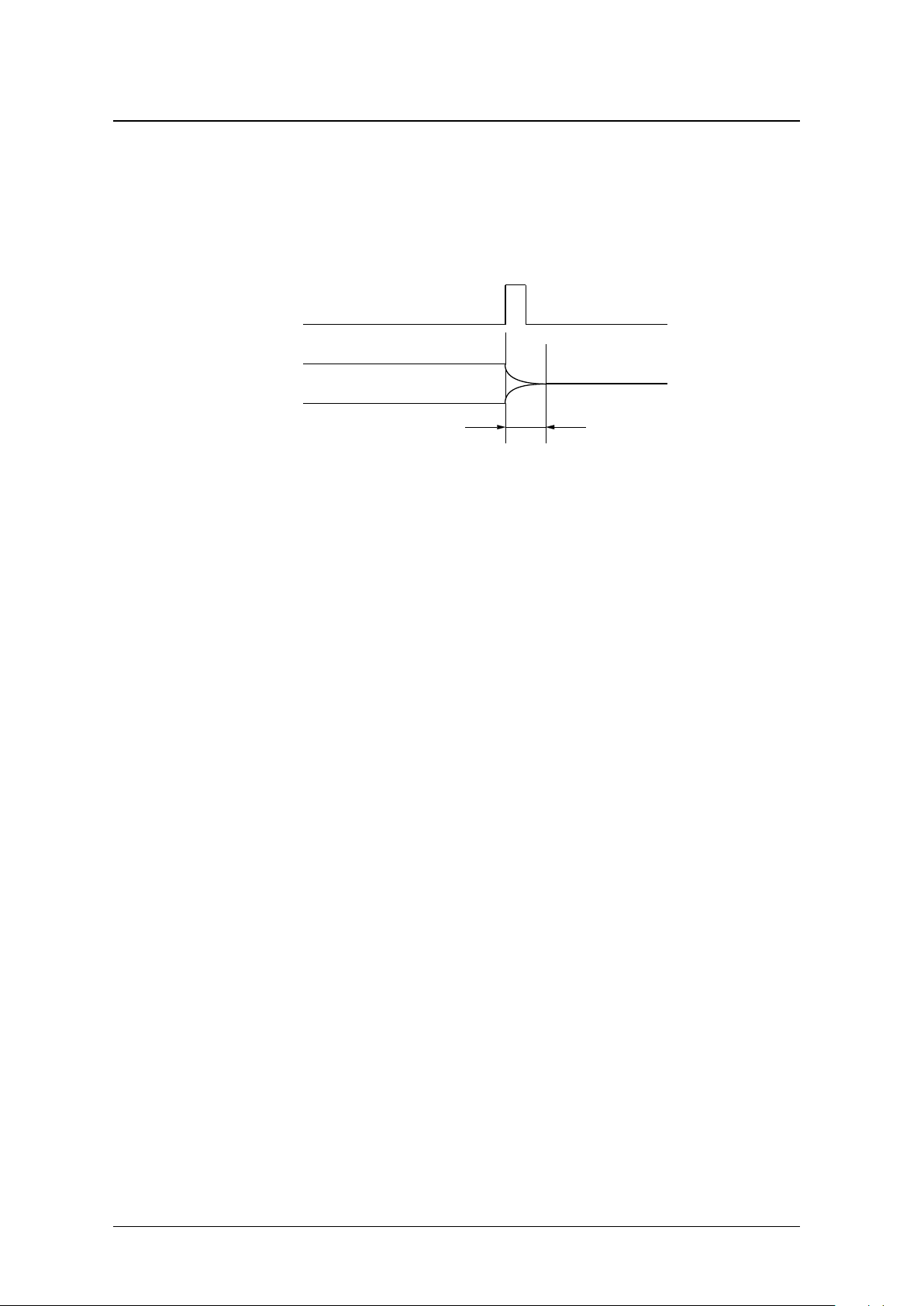
Fast Damping
When melody output stops, the D/A converter output
amplitude does not fall to zero instantaneously,
instead the output converges to zero within a maximum of 8.2 ms to prevent noise being generated.
Also, when one-shot melody output mode is retriggered, melody output restarts after the fast damping
interval.
Note: Refer to the "TIMING DIAGRAMS" section to confirm melody timing specifics
Figure 15. Fast damping timing
STOP
Melody
Output
8.2msec(max)
Page 15

SM1350 series
NIPPON PRECISION CIRCUITS—15
Sound Generator
Synthesis mthod
The sound generators use the dual wave synthesis (DWS) method. The DWS method uses the envelope of 2
waveforms (main waveform and sub waveform) to synthesize the generated tone. Using this method makes
possible high tone quality output that faithfully reproduces the tones of real musical instruments.
Number of simultaneous sounds
The maximum number of tones that can be generated simultaneously is 4, making 4-part harmony
harmony
Generation possible (where each tone is derived from corresponding main and sub waveforms).
Sound range
The range of sounds covers 5 octaves from note G2 to F#7.
Waveform ROM
Waveforms are stored in a 10-bit × 128-word × 8-waveform capacity waveform ROM.
Number of programmable tones
The maximum number of programmable tones is 16. Note that 2 similar tones which have different envelope
settings are considered to be separate tones.
Built-in ROMs
The built-in ROMs comprise 3 types of ROM—waveform ROM containing waveform data, score ROM
containing musical score data, and parameter ROM containing envelope and jump data.
Figure 16.
Generated Sound
Sub Wave
Main Wave
Synthesize
Envelope
Envelope
Page 16

SM1350 series
NIPPON PRECISION CIRCUITS—16
Melodies
Number of melodies
The maximum number of program melodies is 16. Note that is the jump function is used to change the tone or
tempo during melody output, then the maximum number of melodies reduces by the number of times the jump
function was invoked.
Number of program steps
The maximum number of program steps that can be stored in score ROM (notes, rests, jump codes and end
codes) is 1024.
Tempo
The basic quarter note tempo can be set in the range 4.8 to 605.6 in multiples of 4.8.
Note (rest) rhythm values
There are 12 note rhythm values and 13 rest rhythm values that can be used to construct a melody. Also, 2 or
more notes can be combined using ties or slurs.
Table 2. Rhythm values Symbol Note Rest
0123456789ABC
Symbol
Note -
3
x
x
3
e
e
3
q
e. q
3
h
q.hh.w
Rest
3¨3
Å
Å
3
ä
ä
3
Î
äÎ
3
·
Î î î. î
Page 17

SM1350 series
NIPPON PRECISION CIRCUITS—17
TIMING DIAGRAMS(Refer to AC CHARACTERISTICS)
One-shot Melody Mode
Figure 17. One-shot mode (standby to melody start)
Figure 18. One-shot mode (retrigger to melody stop)
ICN
STN
OSC
MODE
LH
S0 to S3
BUSYN
MELODY
OUTPUT
tICW
tXST
tSTW
tDAST
tCH1
tMR
tSR
tBYST
tPYST
#N
#N
STN
STOP
MODE
LH
S0 to S3
Melody
Output
BUSYN
ENDN
OSC
t
STW
tCH2
tMR
tSR
#N
#M
tPYST
tSTPW
tCH2
#N
tBYEN
tEDW
tEDST
tDEAN
tXEN
Page 18

SM1350 series
NIPPON PRECISION CIRCUITS—18
Level Hold Melody Mode 1 (master slice option: “Change select retrigger [Yes]”)
Figure 19. Level hold mode (standby to melody start)
Figure 20. Level hold mode (retrigger to melody stop)
ICN
STN
OSC
MODE
LH
S0 to S3
BUSYN
Melody
Output
t
ICW
t
XST
t
DAST
t
CH1
t
MR
t
SR
t
BYST
t
PYST
#N
#N
STN
S0 to S3
Melody
Output
BUSYN
ENDN
OSC
#M
#M
t
CH3
t
CH2
#N
#N
t
EDST
t
EDW
t
BYEN
t
XEN
t
DAEN
Page 19

SM1350 series
NIPPON PRECISION CIRCUITS—19
Level Hold Melody Mode 2 (master slice option: “Change select retrigger [No]”)
Figure 21. Level hold mode (standby to melody start)
Figure 22. Level hold mode (repeating melody to melody stop)
ICN
STN
OSC
MODE
LH
S0 to S3
BUSYN
Melody
Output
tICW
tXST
tCH1
tDAST
tMR
tSR
#N
tBYST
tPYST
#N
STN
S0 to S3
Melody
Output
BUSYN
ENDN
OSC
tEDW
tCH2
tBYEN
tEDST
tEDW
tDAEN
tXEN
#N #N
Page 20

SM1350 series
NIPPON PRECISION CIRCUITS—20
MEASUREMENT CIRCUIT
Note that circuit constants are reference values.
Parameter Pin name Measurement state
1 Melody output circuit BTL
2 STN Pull-up
3 STOP Pull-up
4 ICN Pull-up
5 LH Pull-up
6 MODE Pull-up
7 S0 to S3 Pull-up
VDD
S0
S1
S2
S3
MODE
LH
STOP
STN
BUSYN
CT
ICN
XT
XTN
TO
T3N
T2N
T1N
NSBN
MSB
SP
SPN
VOL
VSS
0.1µF
200KΩ
4.7 to 10 µF
(Nonpolarity)
4MHz
C
G
C
D
Page 21

SM1350 series
NIPPON PRECISION CIRCUITS—21
NIPPON PRECISION CIRCUITS INC. reserves the right to make changes to the products described in this data sheet in order to
improve the design or performance and to supply the best possible products. Nippon Precision Circuits Inc. assumes no responsibility for
the use of any circuits shown in this data sheet, conveys no license under any patent or other rights, and makes no claim that the circuits
are free from patent infringement. Applications for any devices shown in this data sheet are for illustration only and Nippon Precision
Circuits Inc. makes no claim or warr anty that such applications will be suitab le for the use specified without further testing or modification.
The products described in this data sheet are not intended to use for the apparatus which influence human lives due to the failure or
malfunction of the products. Customers are requested to comply with applicable laws and regulations in effect now and hereinafter,
including compliance with export controls on the distribution or dissemination of the products. Customers shall not export, directly or
indirectly, any products without first obtaining required licenses and approvals from appropriate government agencies.
NIPPON PRECISION CIRCUITS INC.
4-3, 2-chome Fukuzumi
Koto-ku, Tokyo 135-8430, Japan
Telephone: 03-3642-6661
Facsimile: 03-3642-6698
NC9611BE 1998.10
NIPPON PRECISION CIRCUITS INC.
 Loading...